NEC PS2711-1-F3, PS2711-1-F4 Datasheet

DATA SHEET
PHOTOCOUPLER
PS2711-1
HIGH CTR
4-PIN SOP PHOTOCOUPLER
DESCRIPTION
The PS2711-1 is an optically coupled isolator containing a GaAs light emitting diode and an NPN silicon
phototransistor in a plastic SOP for high density applications.
The package is an SOP (Small Outline Package) type for high density mounting applications.
FEATURES
• High current transfer ratio (CTR = 200 % TYP. @ IF = 1mA)
• High isolation voltage (BV = 3 750 Vr.m.s.)
• Small and thin package (4-pin SOP)
• Ordering number of tape product: PS2711-1-F3, F4
• UL approved: File No. E72422 (S)
−NEPOCTM Series−
APPLICATIONS
• Programmable logic controllers
• Small power supply
•Hybrid IC
• Modem/FAX
The information in this document is subject to change without notice. Before using this document, please
confirm that this is the latest version.
Not all devices/types available in every country. Please check with local NEC representative for
availability and additional information.
Document No. P14945EJ1V0DS00 (1st edition)
Date Published July 2000 NS CP(K)
Printed in Japan
©
2000

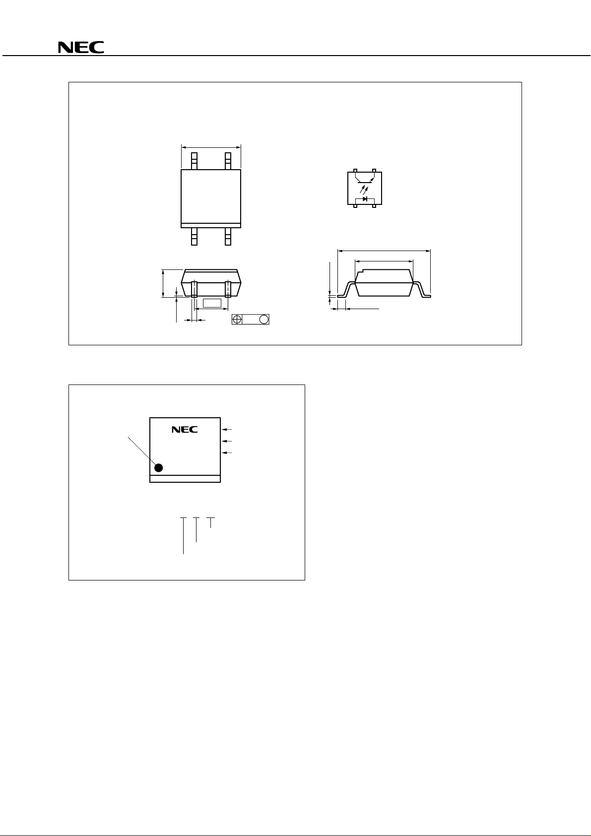
PACKAGE DIMENSIONS
in millimeters
PS2711-1
MARKING
No. 1 pin Mark
2.1±0.2
0.1±0.1
2711
N003
4±0.5
2.54
0.4
+0.10
0.25 M
–0.05
Trade Mark
Type Number
Assembly Lot
+0.10
–0.05
0.15
TOP VIEW
43
12
7.0±0.3
4.4
0.5±0.3
1. Anode
2. Cathode
3. Emitter
4. Collector
N003
Week Assembled
Year Assembled
(Last 1 Digit)
CTR Rank Name
2
Data Sheet P14945EJ1V0DS00

ORDERING INFORMATION
PS2711-1
Part Number Package Packing Style
Safety Standards
Approval
Application Part
Number
PS2711-1 4-pin SOP 50 pcs (Tape 50 pcs cut) UL approved PS2711-1
PS2711-1-F3 Embossed Tape 3 500 pcs/reel
PS2711-1-F4
For the application of the Safety Standard, following part number should be used.
*1
ABSOLUTE MAXIMUM RATINGS (TA = 25 °°°°C, unless otherwise specified)
Parameter Symbol Ratings Unit
Diode Forward Current (DC) I
Reverse Voltage V
Power Dissipation Derati ng∆PD/°C0.8mW/
Power Dissipation P
Peak Forward Current
*1
Transistor Collector to Emitter Voltage V
Emitter to Collector Voltage V
Collector Current I
Power Dissipation Derati ng∆PC/°C1.5mW/
Power Dissipation P
Isolation Voltage
*2
Operating Ambient Temperature T
Storage Temperature T
F
R
50 mA
6V
°
I
D
FP
CEO
ECO
C
80 mW
0.5 A
40 V
5V
40 mA
°
C
150 mW
BV 3 750 Vr.m.s.
A
stg
–55 to +100
–55 to +150
°
C
°
C
C
C
*1
PW = 100
*1
AC voltage for 1 minute at TA = 25 °C, RH = 60 % between input and output
*2
µ
s, Duty Cycle = 1 %
Data Sheet P14945EJ1V0DS00
3

ELECTRICAL CHARACTERISTICS (TA = 25 °°°°C)
Parameter Symbol Conditions MIN. TYP. MAX. Unit
PS2711-1
Diode Forward Voltage V
Reverse Current I
Terminal Capacitance C
Transistor Collector to Emitter Dark
Current
Coupled Current Transf er Rat i o
*1
C/IF
(I
)
CTR IF = 1 mA, VCE = 5 V 100 200 400 %
Collector Saturation Voltage V
Isolation Resistance R
Isolation Capacitance C
*2
*2
CTR rank
*1
Rise Time
Fall Time
N : 100 to 400 (%)
K : 200 to 400 (%)
L : 150 to 300 (%)
M: 100 to 200 (%)
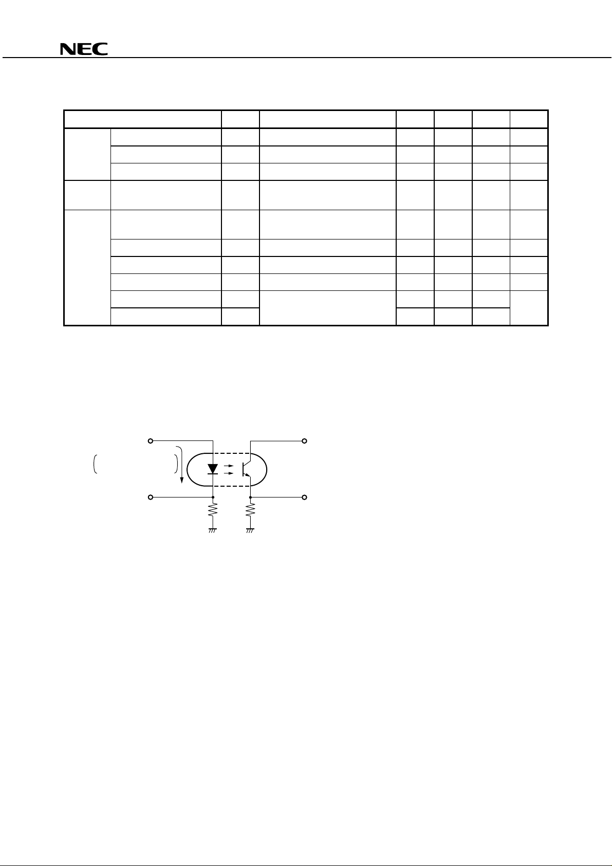
Test circuit for switching time
*2
F
IF = 5 mA 1.15 1.4 V
R
VR = 5 V 5
t
V = 0 V, f = 1 MHz 30 pF
CEOIF
I
CE (sat)IF
t
t
= 0 mA, VCE = 40 V 100 nA
= 1 mA, IC = 0.2 mA 0.3 V
I-O
I-O
V
I-O
V = 0 V, f = 1 MHz 0.4 pF
r
VCC = 5 V, IC = 2 mA, RL = 100
f
= 1 kV
DC
Ω
10
11
4
5
µ
A
Ω
µ
s
Pulse Input
PW = 100 s
µ
Duty cycle = 1/10
In monitor
I
F
50 Ω
RL = 100 Ω
V
CC
V
OUT
4
Data Sheet P14945EJ1V0DS00
 Loading...