

DATA SHEET
PHOTOCOUPLER
PS2705-1,PS2705-2,PS2705-4
HIGH ISOLATION VOLTAGE
AC INPUT RESPONSE TYPE
SOP MULTI PHOTOCOUPLER
DESCRIPTION
The PS2705-1, PS2705-2, PS2705-4 are optically coupled isolators containing two GaAs light emitting diodes and
an NPN silicon phototransistor.
These packages are SOP (Small Outline Package) type and have shield effect to cut off ambient light.
They are designed for high density mounting applications.
FEATURES
• AC input response
• High isolation voltage (BV = 3 750 Vr.m.s.)
• High current transfer ratio (CTR = 100 % TYP.)
• SOP (Small Outline Package) type
• High-speed switching (tr = 3 µs TYP., tf = 5 µs TYP.)
• Ordering number of taping product (Only-1 type) : PS2705-1-E3, E4, F3, F4
• UL approved: File No. E72422 (S)
• VDE0884 approved (Option)
−NEPOCTM Series−
APPLICATIONS
•Hybrid IC
• Telephone/FAX
• FA/OA equipment
• Programmable logic controllers
• Power supply
ORDERING INFORMATION
Part Number Package Safety Standard Approval
PS2705-1 4-pin SOP Standard products
PS2705-2 8-pin SOP • UL approved
PS2705-4 16-pin SOP
PS2705-1-V 4-pin SOP VDE0884 approved products (Option)
PS2705-2-V 8-pin SOP
PS2705-4-V 16-pin SOP
The information in this document is subject to change without notice.
Document No. P11309EJ5V0DS00 (5th edition)
Date Published December 1998 NS CP (K)
Printed in Japan
The mark
••••
shows major revised points.
©
1988
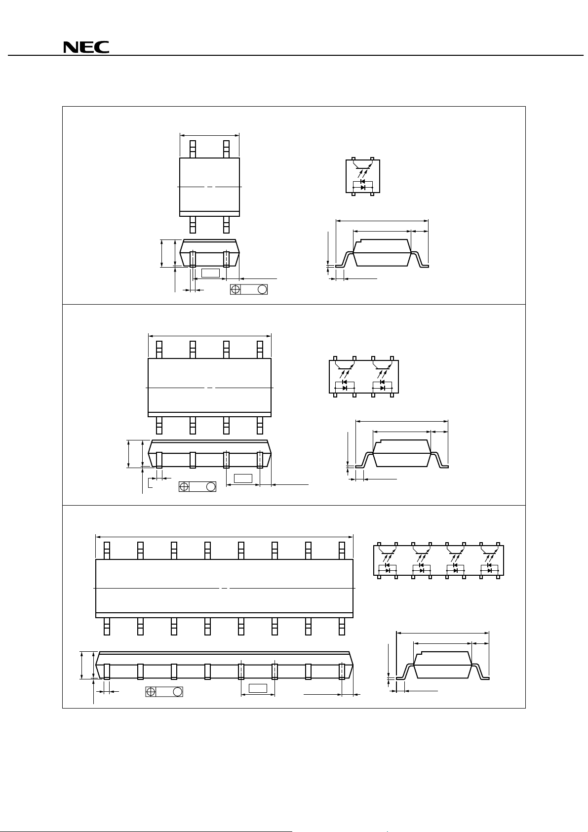
PACKAGE DIMENSIONS (in millimeters)
PS2705-1,PS2705-2,PS2705-4
2.0
2.3 MAX.
0.1±0.1
2.0
2.3 MAX.
0.1±0.1
+0.10
0.4
–0.05
4.5 MAX.
2.54
0.4
9.3 MAX.
0.25 M
+0.10
–0.05
1.2 MAX.
0.25 M
2.54
PS2705-1
PS2705-2
1.2 MAX.
TOP VIEW
43
12
7.0±0.3
4.4
+0.10
–0.05
0.15
0.5±0.3
TOP VIEW
8765
1234
+0.10
–0.05
0.15
0.5±0.3
1. Anode, Cathode
2. Cathode, Anode
3. Emitter
4. Collector
1.3
1. 3. Anode, Cathode
2. 4. Cathode, Anode
5. 7. Emitter
6. 8. Collector
7.0±0.3
4.4
1.3
2
2.0
2.3 MAX.
0.1±0.1
0.4
+0.10
–0.05
0.25 M
19.46 MAX.
PS2705-4
2.54
Data Sheet P11309EJ5V0DS00
1.2 MAX.
TOP VIEW
16 15 14 13 12 11 10 9
2345678
1
1. 3. 5. 7. Anode, Cathode
2. 4. 6. 8. Cathode, Anode
9. 11. 13. 15. Emitter
10. 12. 14. 16. Collector
7.0±0.3
1.3
+0.10
–0.05
0.15
4.4
0.5±0.3
PS2705-1,PS2705-2,PS2705-4
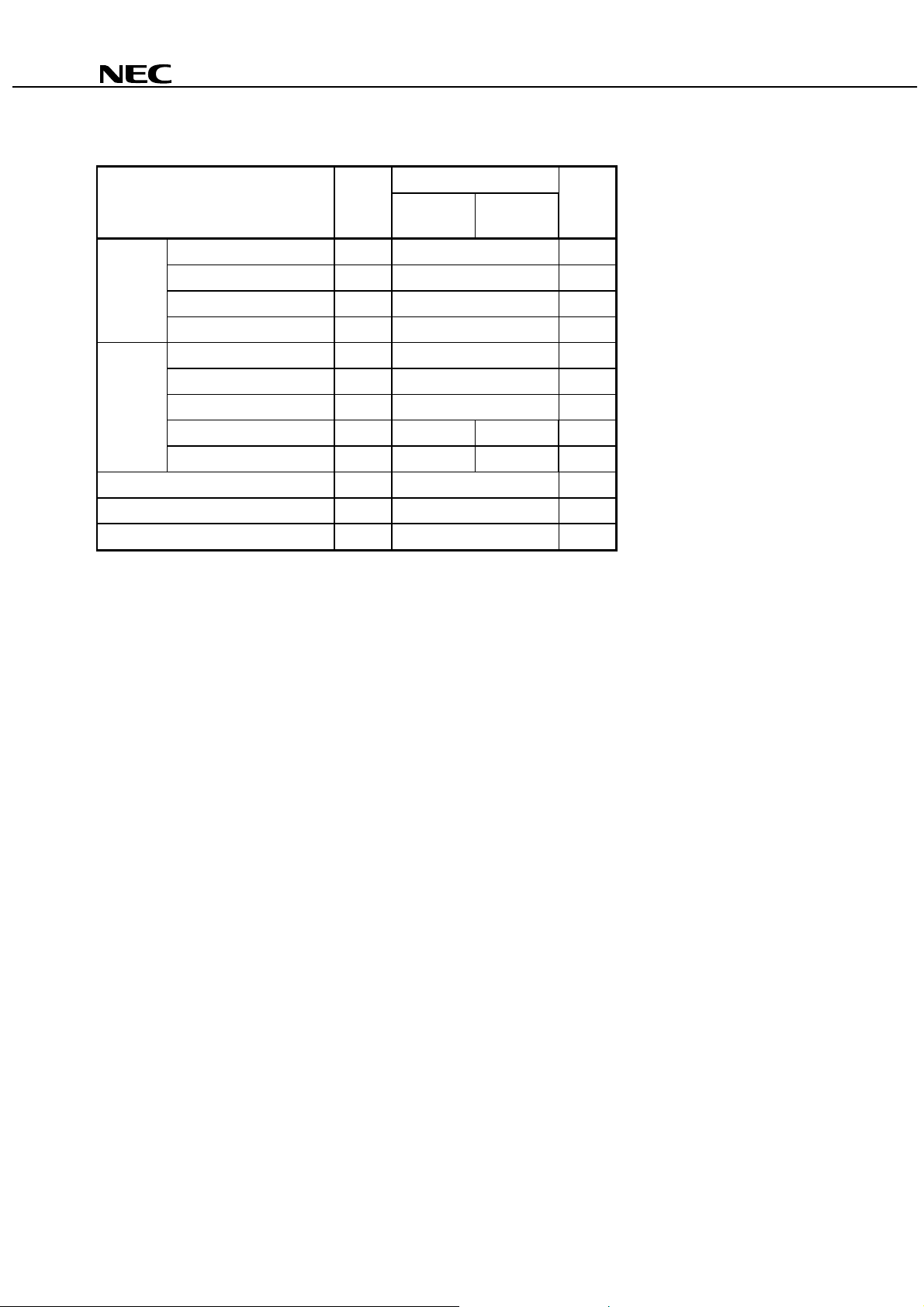
ABSOLUTE MAXIMUM RATINGS (TA = 25 °°°°C, unless otherwise specified)
Ratings
Parameter Symbol PS2705-1 PS2705-2,
PS2705-4
Unit
Diode Forward Current (DC) I
F
±
50 mA
Power Dissipation Derati ng∆PD/°C0.8mW/
I
FP
CEO
ECO
C
D
80 mW/ch
±
1A
40 V
6V
80 mA/ch
Power Dissipation P
Peak Forward Current
*1
Transistor Collector to Emitter Voltage V
Emitter to Collector Voltage V
Collector Current I
Power Dissipation Derati ng∆PC/°C 1.5 1.2 mW/°C
Power Dissipation P
Isolation Voltage
*2
Operating Ambient Temperature T
Storage Temperature T
PW = 100
*1
AC voltage for 1 minute at TA = 25 °C, RH = 60 % between input and output
*2
µ
s, Duty Cycle = 1 %
C
150 120 mW/ch
BV 3 750 Vr.m . s.
A
stg
–55 to +100
–55 to +150
°
C
°
C
°
C
Data Sheet P11309EJ5V0DS00
3
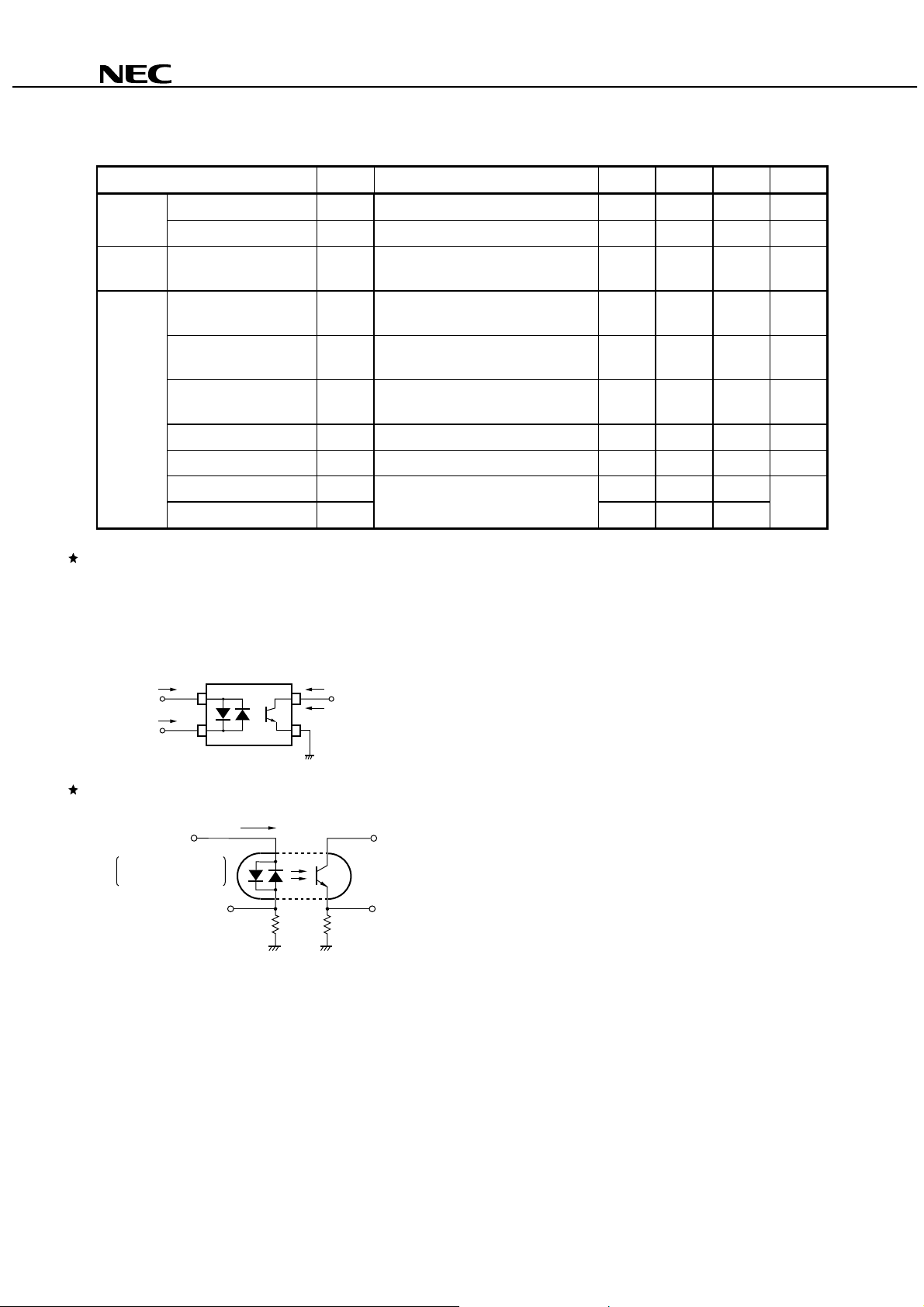
ELECTRICAL CHARACTERISTICS (TA = 25 °°°°C)
Parameter Symbol Conditions MIN. TYP. MAX. Unit
PS2705-1,PS2705-2,PS2705-4
Diode Forward Voltage V
Terminal Capacitance C
Transistor Collector to Emitter
Current
Coupled Current Transfer Ratio
*1
C/IF
)
(I
CTR IF = ± 5 mA, VCE = 5 V 50 100 300 %
CTR Ratio CTR1/
CTR
Collector Satura tio n
V
Voltage
Isolation Resistance R
Isolation Capacitance C
Rise Time
Fall Time
CTR rank (only PS2705-1)
*1
*2
*2
M: 50 to 150 (%)
L: 100 to 300 (%)
N: 50 to 300 (%)
*2
1
CTR
= IC1/IF1, CTR2 = IC2/I
F2
F
IF = ± 5 mA 1.1 1.4 V
t
V = 0 V, f = 1 MHz 60 pF
CEOIF
I
= 0 mA, VCE = 40 V 100 nA
IF = ± 5 mA, VCE = 5 V 0.3 1.0 3.0
2
CE (sat)IF
t
t
= ± 10 mA, IC = 2 mA 0.3 V
I-O
I-O
V
I-O
V = 0 V, f = 1 MHz 0.4 pF
r
VCC = 5 V, IC = 2 mA, RL = 100
f
= 1 kV
DC
Ω
10
11
3
5
Ω
µ
s
I
F1
I
F2
Test circuit for switching time
*3
I
Pulse Input
PW = 100 s
µ
F
Duty Cycle = 1/10
In monitor
50 Ω
I
C1
I
C2
V
CE
V
V
RL = 100 Ω
CC
OUT
4
Data Sheet P11309EJ5V0DS00
 Loading...