

NEC PS2625, PS2625L, PS2626, PS2626L Datasheet
DATA SHEET
PHOTOCOUPLER
PS2625, PS2626, PS2625L, PS2626L
HIGH ISOLATION VOLTAGE AC INPUT
LARGE FORWARD AC INPUT TYPE
6 PIN PHOTOCOUPLER
DESCRIPTION
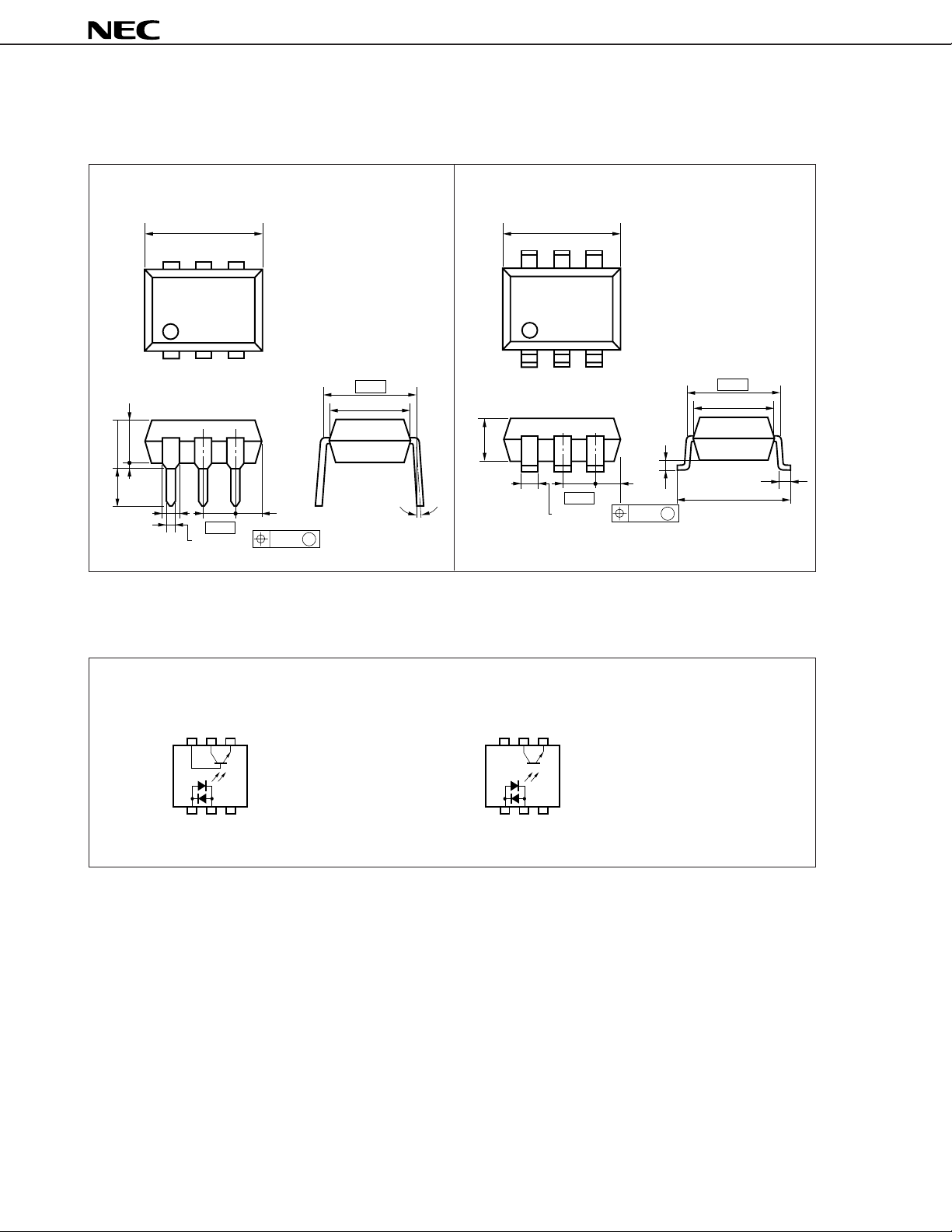
PS2625, PS2626 and PS2625L, PS2626L are optically coupled isolators containing a GaAs light emitting diode
and an NPN silicon phototransistor.
PS2625, PS2626 are in a plastic DIP (Dual In-line Package).
PS2625L, PS2626L are lead bending type (Gull-wing) for surface mount.
PS2625, PS2625L have base pin and PS2622, PS2622L have no base pin.
FEATURES
• High isolation voltage (BV: 5 kVr.m.s. MIN.)
• AC input response
• Large forward input (current) (I
• High collector to emitter voltage (VCEO: 80 V MIN.)
• High speed switching (t
• UL recognized [File No. E72422(S)]
• Taping product name (PS2625L-E3, E4, PS2626L-E3, E4)
r = 3
F: ±150 mA MAX.)
µ
s, tf = 5 µs TYP.)
— NEPOC Series —
APPLICATIONS
Interface circuit for various instrumentations, control equipments.
• AC Line/Digital Logic............................................................ Isolate high voltage transient
• Digital Logic/Digital Logic..................................................... Eliminate spurious ground loops
• Twisted pair line receiver ..................................................... Eliminate ground loop pick-up
• Telephone/Telegraph line receiver ...................................... Isolate high voltage transient
• High Frequency Power Supply Feedback Control.............. Maintain floating ground
Document No. P11293EJ3V0DS00 (3rd edition)
(Previous No. LC-2125A)
Date Published February 1996 P
Printed in Japan
©
1988
PS2625, PS2626, PS2625L, PS2626L
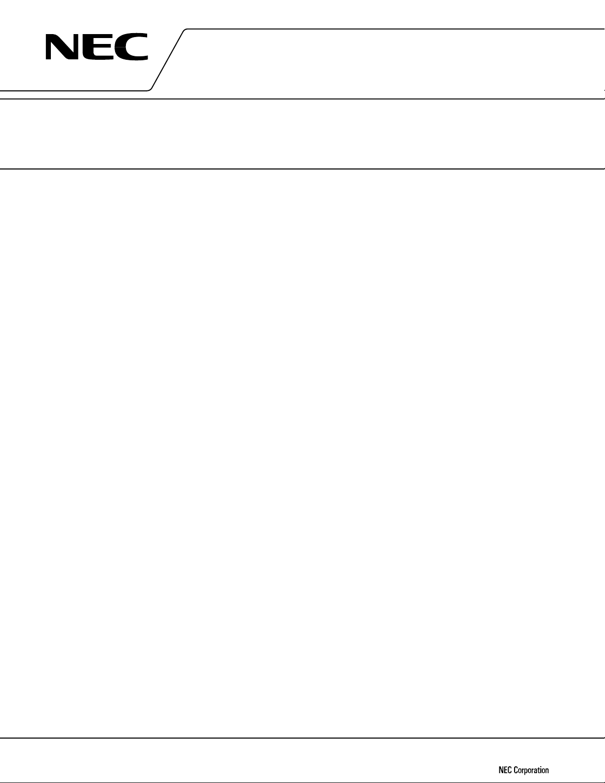
PACKAGE DIMENSIONS (Unit: mm)
DIP (Dual In-line Package) Lead Bending type (Gull-wing)
PS2625, PS2626 PS2625L, PS2626L
10.16 MAX.
64
1 3
3.8
MAX.
0.65
2.8 MIN. 4.55 MAX.
1.34
2.54
0.50 ±0.10
2.54
MAX.
0.25 M
PIN CONNECTION (Top View)
7.62
6.5
0 to 15˚
3.8 MAX.
10.16 MAX.
64
1 3
2.54
2.54
1.34 ±0.10
MAX.
0.25 M
7.62
6.5
0.05 to 0.2
0.9 ±0.25
9.60 ±0.4
PS2625, PS2625L PS2626, PS2626L
654
123
1. Anode, Cathode
2. Cathode, Anode
3. NC
4. Emitter
5. Collector
6. Base
654
123
1. Anode, Cathode
2. Cathode, Cathode
3. NC
4. Emitter
5. Collector
6. NC
2
PS2625, PS2626, PS2625L, PS2626L
ABSOLUTE MAXIMUM RATINGS (TA = 25 ˚C)
Diode
Forward Current (DC) IF ±150 mA
Power Dissipation Derating ∆PD/˚C 2.0 mW/˚C
Power Dissipation P
Peak Forward Current IF(Peak) ±1A
(PW = 100 µs, Duty Cycle 1 %)
Transistor
Collector to Emitter Voltage V
Emitter to Collector Voltage VECO 7V
Collector Current I
Power Dissipation Derating ∆PC/˚C 1.5 mW/˚C
Power Dissipation PC 150 mW
Coupled
Isolation Voltage *
1)
Storage Temperature Tstg –55 to +150 ˚C
Operating Temperature T
D 200 mW
CEO 80 V
C 50 mA
BV 5 000 Vr.m.s.
opt –55 to +100 ˚ C
*1) AC voltage for 1 minute at TA = 25 ˚C, RH = 60 % between input (Pin No. 1, 2, 3, Common) and output (Pin No.
4, 5, 6 Common).
ELECTRICAL CHARACTERISTICS (TA = 25 ˚C)
CHARACTERISTIC SYMBOL MIN. TYP. MAX. UNIT TEST CONDITIONS
Diode Forward Voltage VF 1.3 1.7 V IF = ±100 mA
Junction Capacitance C 140 pF V = 0, f = 1.0 MHz
Transistor Collector to Emitter Dark ICEO 100 nA VCE = 80 V, IF = 0
Current
DC Current Gain*
Coupled Current Transfer Ratio CTR 20 50 % IF = ±100 mA, VCE = 3 V
CTR Ratio
Collector Saturation Voltage
Isolation Resistance R1-2 10
Isolation Capacitance C1-2 0.6 pF V = 0, f = 1.0 MHz
Rise Time*
Fall Time*
2)
3)
*
4)
4)
hFE 700 IC = 2 mA, VCE = 5 V
CTR1/CTR2
VCE(sat) 0.3 V IF = ±100 mA, IC = 4 mA
tr 3
tf 5
0.3 1.0 3.0 IF = ±100 mA, VCE = 3 V
11
Ω Vin-out = 1.0 kV
µ
s
VCC = 5 V, IC = 2 mA, RL = 100 Ω
µ
s
VCC = 5 V, IC = 2 mA, RL = 100 Ω
*2) PS2625, PS2625L only *4) Test Circuit for Switching Time
I
*3)
CTR1 =
IF1
IF2
C1
I
, CTR2 =
IC2
IF1 IF2
IC1
IC2
PULSE INPUT
PW = 100 s
Duty Cycle = 1/10
µ
F
50 Ω
V
V
RL = 100 Ω
CC
OUT
3
 Loading...