

Page 1

PRELIMINARY PRODUCT INFORMATION
MOS INTEGRATED CIRCUIT
µ
PD78F0058Y
8-BIT SINGLE-CHIP MICROCONTROLLER
DESCRIPTION
The µPD78F0058Y is a product of the µPD780058Y Subseries in the 78K/0 Series and equivalent to the
µ
PD780058Y with a flash memory in place of internal ROM. This device is incorporated with a flash memory which
can be programmed without being removed from the substrate.
Functions are described in detail in the following user’s manuals, which should be read when carrying out
design work.
µ
PD780058, 780058Y Subseries User’s Manual : U12013E
78K/0 Series User’s Manual Instruction : U12326E
FEATURES
• Pin-compatible with mask ROM versions (except VPP pin)
• Flash memory : 60 Kbytes
• Internal high-speed RAM : 1024 bytes
• Internal expansion RAM : 1024 bytes
• Buffer RAM : 32 bytes
• Operable with the same power supply voltage as that of mask ROM version (V
Notes 1. The flash memory capacity can be changed with the memory size switching register (IMS).
2. The internal expansion RAM capacity can be changed with the internal expansion RAM size
switching register (IXS).
Remark For the differences between the flash memory versions and the mask ROM versions, refer to
1. DIFFERENCES BETWEEN
Note 1
Note 2
µ
PD78F0058Y AND MASK ROM VERSIONS.
DD = 1.8 to 5.5 V)
ORDERING INFORMATION
Part Number Package Internal ROM
µ
PD78F0058YGC-3B9
µ
PD78F0058YGC-8BT
µ
PD78F0058YGK-BE9
Note
Note
Note
80-pin plastic QFP (14 × 14 mm, resin thickness 2.7 mm) Flash memory
80-pin plastic QFP (14 × 14 mm, resin thickness 1.4 mm) Flash memory
80-pin plastic TQFP (fine pitch) (12 × 12 mm) Flash memory
Note Under planning
Caution Two types of packages are available for
For the suppliable package, consult an NEC sales representative.
The information contained in this document is being issued in advance of the production cycle for the
device. The parameters for the device may change before final production or NEC Corporation, at its own
discretion, may withdraw the device prior to its production.
Document No. U12324EJ1V0PM00 (1st edition)
Date Published April 1997 N
Printed in Japan
µ
PD78F0058YGC (refer to 6. PACKAGE DRAWINGS).
©
1997
Page 2
µ
PD78F0058Y
78K/0 SERIES DEVELOPMENT
The products in the 78K/0 series are listed below. The names enclosed in boxes are subseries names.
Under mass production
Under development
78K/0
series
For Control
Note
TM
µ
µ
µµ
µµ
PD780018Y
PD780058Y
µ
µ
µ
µ
µ
µ
µ
µ
Note
Note
100 pins Low EMI noise model of the PD78078PD78075BµPD78075BY
100 pins
100 pins
100 pins
80 pins Enhanced serial I/O of the PD78054, low EMI noise model
80 pins
80 pins
64 pins
64 pins
64 pins
80 pins Basic subseries for driving FIP; Total number of display outputs: 34
PD78078µPD78078Y
PD78070A PD78070AY
PD780018
µ
PD780058
µ
PD78058F PD78058FY
PD78054 PD78054Y
µ
µ
PD780034 PD780034Y
µ
PD780024 PD780024Y
PD78014H64 pins Low EMI noise model of the PD78018F
µ
PD78018F64 pins PD78018FY
µ
µ
PD7801464 pins PD78014Y
µ
PD78000164 pins
µ
PD7800264 pins PD78002Y
µ
PD78083
For Inverter Control
µ
PD78096464 pins
µ
PD780924
For Driving FIP
µ
PD780208100 pins
µ
PD780228100 pins
PD78044H80 pins
µ
PD78044F
µ
Y subseries supports I
Adds timer to the PD78054 with enhanced external interface function
ROM-less model of the PD78078
Enhanced serial I/O of the PD78078 with limited function
Low EMI noise model of the PD78054
Adds UART and D/A to the PD78014 with enhanced I/O
Enhanced A/D of the PD780024
Enhanced serial I/O of the PD78018F, low EMI noise model
Low-voltage model (1.8 V) of the PD78014 with increased choice of ROM and RAM capacities
Adds A/D and 16-bit timer to the PD78002
Adds A/D to the PD78002
Basic subseries for control applications
UART provided, low-voltage (1.8 V) operation42/44 pins
Enhanced A/D of the PD780924
Inverter control circuit and UART provided, low EMI noise model
Enhanced l/O, FIP C/D of the PD78044F; Total number of display outputs: 53
Enhanced I/O, FIP C/D of the PD78044H; Total number of display outputs: 48
Adds N-ch open drain I/O to the PD78044; Total number of display outputs: 34
µ
µ
2
C bus.
µ
µ
µ
µ
µ
µ
µ
µ
µ
µ
µ
µ
µ
µ
µ
100 pins
Note Under planning
2
For Driving LCD
µ
PD780308100 pins
PD78064B100 pins
µ
PD78064 PD78064Y
µ
Supporting IEBus
PD7809880 pins
µ
For LV
PD78P091464 pins
µ
TM
PD780308Y
µ
µ
Enhanced SIO of the PD78064 with extended ROM and RAM
Low EMI noise model of the PD78064
Subseries for driving LCD with UART provided
Adds IEBus controller to the PD78054
PWM output, LV digital code decoder, and Hsync counter provided
µ
µ
µ
Page 3
µ
PD78F0058Y
Major functional differences among the Y subseries are shown below.
Function ROM Capacity Serial Interface I/O VDD MIN.
Subseries Value
Control
LCD
control 3-wire/time division UART : 1ch
µ
PD78075BY 32 K to 40 K 3-wire/2-wire/I2C : 1ch 88 1.8 V
µ
PD78078Y 48 K to 60 K
µ
PD78070AY – 61 2.7 V
µ
PD780018Y 48 K to 60 K
µ
PD780058Y 24 K to 60 K 3-wire/2-wire/I2C : 1ch 68 1.8 V
µ
PD78058FY 48 K to 60 K 3-wire/2-wire/I2C : 1ch 69 2.7 V
µ
PD78054Y 16 K to 60 K 3-wire/UART : 1ch 2.0 V
µ
PD780034Y 8 K to 32 K UART : 1ch 51 1.8 V
µ
PD780024Y I2C bus (supports multimaster) : 1ch
µ
PD78018FY 8 K to 60 K 3-wire/2-wire/I2C : 1ch 53
µ
PD78014Y 8 K to 32 K 3-wire/2-wire/SBI/I2C : 1ch 2.7 V
µ
PD78002Y 8 K to 16 K 3-wire/2-wire/SBI/I2C : 1ch
µ
PD780308Y 48 K to 60 K 3-wire/2-wire/I2C : 1ch 57 2.0 V
µ
PD78064Y 16 K to 32 K 3-wire/2-wire/I2C : 1ch
3-wire with automatic send/receive function
3-wire/UART : 1ch
3-wire with automatic send/receive function
Time division UART : 1ch
2
C bus (supports multimaster) : 1ch
I
3-wire with automatic send/receive function
3-wire/time division UART : 1ch
3-wire with automatic send/receive function
3-wire : 1ch
3-wire with automatic send/receive function
3-wire with automatic send/receive function
3-wire : 1ch
3-wire/UART : 1ch
: 1ch
: 1ch 88
: 1ch
: 1ch
: 1ch
: 1ch
Remark The functions, except for the serial interface are the same as those of subseries without Y.
3
Page 4
µ
OVERVIEW OF FUNCTION
Item Function
Internal Flash memory 60 Kbytes
memory
Memory space 64 Kbytes
General-purpose registers 8 bits × 32 registers (8 bits × 8 registers × 4 banks)
Instruction cycle On-chip instruction execution time cycle modification function
Instruction set • 16-bit operation
I/O ports Total : 68
A/D converter • 8-bit resolution × 8 channels
D/A converter • 8-bit resolution × 2 channels
Serial interface • 3-wired serial I/O/2-wire serial I/O/I
Timer • 16-bit timer/event counter : 1 channel
Timer output 3 (14-bit PWM output capable: 1)
Clock output 19.5 kHz, 39.1 kHz, 78.1 kHz, 156 kHz, 313 kHz, 625 kHz, 1.25 MHz, 2.5 MHz,
Buzzer output 1.2 kHz, 2.4 kHz, 4.9 kHz, 9.8 kHz (main system clock: at 5.0-MHz operation)
Vectored-interrupt Maskable Internal : 13, External : 7
source Non-maskable Internal : 1
Test input Internal : 1, External : 1
Power supply voltage VDD = 1.8 to 5.5 V
Operating ambient temperature TA = –40 to +85°C
Package • 80-pin plastic QFP (14 × 14 mm, resin thickness 2.7 mm)
High-speed RAM 1024 bytes
Expansion RAM 1024 bytes
Buffer RAM 32 bytes
When main system 0.4
clock selected
When subsystem 122
clock selected
• Multiplication/division (8 bits × 8 bits,16 bits ÷ 8 bits)
• Bit manipulation (set, reset, test, boolean operation)
• BCD correction, etc.
• CMOS input : 2
• CMOS I/O : 62
• N-ch open drain I/O : 4
• 3-wired serial I/O mode (MAX. 32-byte on-chip automatic
send/receive function) : 1 channel
• 3-wired serial I/O/UART mode (on-chip time division transfer function)
selectable : 1 channel
• 8-bit timer/event counter : 2 channels
• Watch timer : 1 channel
• Watchdog timer : 1 channel
5.0 MHz (main system clock: at 5.0-MHz operation)
32.768 kHz (subsystem clock: at 32.768-kHz operation)
Software 1
• 80-pin plastic QFP (14 × 14 mm, resin thickness 1.4 mm)
• 80-pin plastic TQFP (fine pitch) (12 × 12 mm)
Notes 1. The flash memory capacity can be changed with the memory size switching register (IMS).
2. The internal expansion RAM capacity can be changed with the internal expansion RAM size
switching register (IXS).
3. Under planning
Note 1
Note 2
µ
s/0.8 µs/1.6 µs/3.2 µs/6.4 µs/12.8 µs (at 5.0-MHz operation)
µ
s (at 32.768-kHz operation)
2
C bus mode selectable : 1 channel
Note 3
Note 3
Note 3
PD78F0058Y
4
Page 5
PIN CONFIGURATION (Top View)
• 80-pin plastic QFP (14 × 14 mm, resin thickness 2.7 mm)
µ
PD78F0058YGC-3B9
• 80-pin plastic QFP (14 × 14 mm, resin thickness 1.4 mm)
µ
PD78F0058YGC-8BT
• 80-pin plastic TQFP (fine pitch) (12 × 12 mm)
µ
PD78F0058YGK-BE9
Note
Note
Note
µ
PD78F0058Y
P15/ANI5
P16/ANI6
P17/ANI7
AV
P130/ANO0
P131/ANO1
REF1
AV
P70/SI2/RxD0
P71/SO2/TxD0
P72/SCK2/ASCK
P20/SI1
P21/SO1
P22/SCK1
P23/STB/TxD1
P24/BUSY/RxD1
P25/SI0/SB0/SDA0
P26/SO0/SB1/SDA1
P27/SCK0/SCL
P40/AD0
P41/AD1
P14/ANI4
P13/ANI3
P12/ANI2
80 79 78 77 76 75 74 73 72 71 70 69 68 67 66 65 64 63 62 61
1
2
3
SS
4
5
6
7
8
9
10
11
12
13
14
15
16
17
18
19
20
21 22 23 24 25 26 27 28 29 30 31 32 33 34 35 36 37 38 39 40
P11/ANI1
P10/ANI0
REF0
AV
VDD0
XT1/P07
XT2
VPPX1X2V
DD1
VSS0
P05/INTP5
P04/INTP4
P03/INTP3
P02/INTP2
P01/INTP1/TI01
P00/INTP0/TI00
60
59
58
57
56
55
54
53
52
51
50
49
48
47
46
45
44
43
42
41
RESET
P127/RTP7
P126/RTP6
P125/RTP5
P124/RTP4
P123/RTP3
P122/RTP2
P121/RTP1
P120/RTP0
P37
P36/BUZ
P35/PCL
P34/TI2
P33/TI1
P32/TO2
P31/TO1
P30/TO0
P67/ASTB
P66/WAIT
P65/WR
P42/AD2
Note Under planning
Cautions 1. Connect the V
2. Connect the AV
Remark When the
µ
PD78F0058Y is used in application fields that require reduction of the noise generated
from inside the microcontroller, the implementation of noise reduction measures, such as supplying
voltage to V
DD0 and VDD1 individually and connecting VSS0 and VSS1 to different ground lines, is
recommended.
SS1
V
P50/A8
P51/A9
P52/A10
P53/A11
P54/A12
P43/AD3
P44/AD4
P45/AD5
P46/AD6
P47/AD7
PP pin directly to VSS0 in normal operation mode
SS pin to VSS0.
P55/A13
P56/A14
P57/A15
P60
P61
P62
P63
P64/RD
5
Page 6

µ
PD78F0058Y
A8 to A15 : Address Bus
AD0 to AD7 : Address/Data Bus
ANI0 to ANI7 : Analog Input
ANO0, ANO1 : Analog Output
ASCK : Asynchronous Serial Clock
ASTB : Address Strobe
REF0, 1 : Analog Reference Voltage
AV
SS : Analog Ground
AV
BUSY : Busy
BUZ : Buzzer Clock
INTP0 to INTP6
: Interrupt from Peripherals
P00 to P05, P07: Port0
P10 to P17 : Port1
P20 to P27 : Port2
P30 to P37 : Port3
P40 to P47 : Port4
P50 to P57 : Port5
P60 to P67 : Port6
P70 to P72 : Port7
P120 to P127 : Port12
P130, P131 : Port13
PCL : Programmable Clock
RD : Read Strobe
RESET : Reset
RTP0 to RTP7 : Real-Time Output Port
RxD0, RxD1 : Receive Data
SB0, SB1 : Serial Bus
SCK0 to SCK2 : Serial Clock
SCL : Serial Clock
SDA0, SDA1 : Serial Data
SI0 to SI2 : Serial Input
SO0 to SO2 : Serial Output
STB : Strobe
TI00, TI01 : Timer Input
TI1, TI2 : Timer Input
TO0 to TO2 : Timer Output
TxD0, TxD1 : Transmit Data
DD0, VDD1 : Power Supply
V
PP : Programming Power Supply
V
SS0, VSS1 : Ground
V
WAIT : Wait
WR : Write Strobe
X1, X2 : Crystal (Main system Clock)
XT1, XT2 : Crystal (Subsystem Clock)
6
Page 7
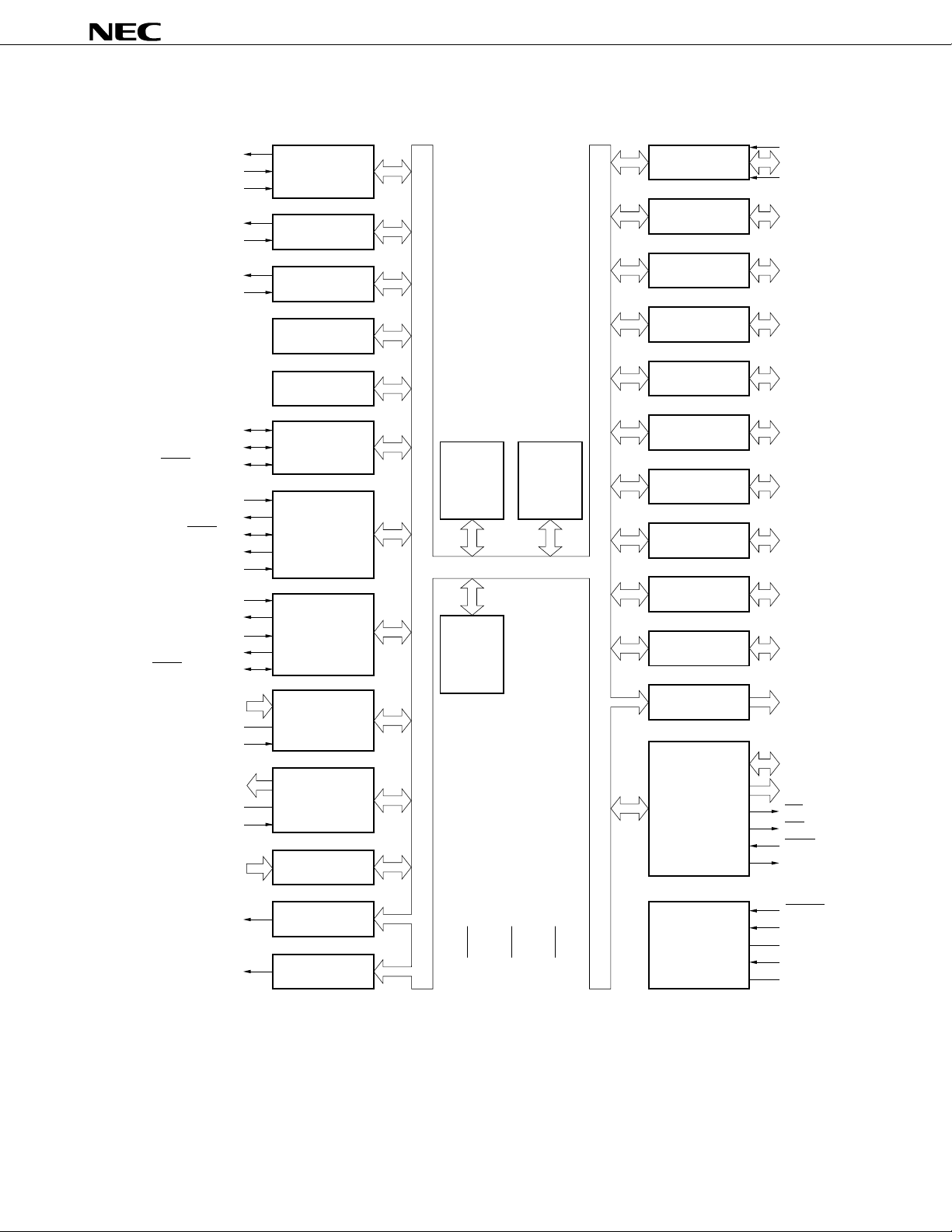
BLOCK DIAGRAM
µ
PD78F0058Y
TO0/P30
TI00/INTP0/P00
TI01/INTP1/P01
TO1/P31
TI1/P33
TO2/P32
TI2/P34
SI0/SB0/SDA0/P25
SO0/SB1/SDA1/P26
SCK0/SCL/P27
SI1/P20
SO1/P21
SCK1/P22
STB/TxD1/P23
BUSY/RxD1/P24
BUSY/RxD1/P24
STB/TxD1/P23
SI2/RxD0/P70
SO2/TxD0/P71
SCK2/ASCK/P72
ANI0/P10 to
ANI7/P17
AV
SS
AV
REF0
ANO0/P130,
ANO1/P131
AV
SS
AV
REF1
INTP0/P00 to
INTP5/P05
16-bit TIMER/
EVENT COUNTER
8-bit TIMER/
EVENT COUNTER 1
8-bit TIMER/
EVENT COUNTER 2
WATCHDOG TIMER
WATCH TIMER
SERIAL
INTERFACE 0
SERIAL
INTERFACE 1
SERIAL
INTERFACE 2
A/D CONVERTER
D/A CONVERTER
INTERRUPT
CONTROL
78K/0
CPU CORE
RAM
2048 Bytes
FLASH
MEMORY
60 K Bytes
PORT0
P01 to P05
P07
P00
PORT1
P10 to P17
PORT2 P20 to P27
PORT3
PORT4
P30 to P37
P40 to P47
PORT5 P50 to P57
PORT6 P60 to P67
PORT7
PORT12
PORT13
REAL-TIME
OUTPUT PORT
P70 to P72
P120 to P127
P130,P131
RTP0/P120 to
RTP7/P127
AD0/P40 to
AD7/P47
A8/P50 to
EXTERNAL
ACCESS
A15/P57
RD/P64
WR/P65
WAIT/P66
ASTB/P67
BUZ/P36
PCL/P35
BUZZER OUTPUT
CLOCK OUTPUT
CONTROL
RESET
SYSTEM
CONTROL
DD0
,
V
SS0
,
V
V
V
DD1
V
SS1
PP
X1
X2
XT1/P07
XT2
7
Page 8

µ
PD78F0058Y
CONTENTS
1. DIFFERENCES BETWEEN µPD78F0058Y AND MASK ROM VERSIONS .................................... 9
2. PIN FUNCTIONS............................................................................................................................... 10
2.1 Port Pins................................................................................................................................................... 10
2.2 Non-Port Pins .......................................................................................................................................... 12
2.3 Pin I/O Circuits and Recommended Connection of Unused Pins ...................................................... 14
3. MEMORY SIZE SWITCHING REGISTER (IMS)............................................................................... 18
4. INTERNAL EXPANSION RAM SIZE SWITCHING REGISTER (IXS) .............................................. 19
5. FLASH MEMORY PROGRAMMING ................................................................................................ 20
5.1 Selection of Transmission Method ........................................................................................................ 20
5.2 Function of Flash Memory Programming ............................................................................................. 21
5.3 Connection of Flashpro II....................................................................................................................... 22
6. PACKAGE DRAWINGS .................................................................................................................... 24
APPENDIX A. DEVELOPMENT TOOLS................................................................................................ 27
APPENDIX B. RELATED DOCUMENTS ............................................................................................... 29
8
Page 9
µ
PD78F0058Y
1. DIFFERENCES BETWEEN µPD78F0058Y AND MASK ROM VERSIONS
The µPD78F0058Y is a product provided with a flash memory which enables on-board reading, erasing, and
µ
rewriting of programs with device mounted on target system. The functions of the
functions specified for flash memory and mask option of P60 to P63 pins) can be made the same as those of the
mask ROM versions by setting the memory size switching register (IMS) and internal expansion RAM size
switching register (IXS).
µ
Table 1-1 shows the differences between the flash memory version (
µ
versions (
PD780053Y, 780054Y, 780055Y, 780056Y, and 780058Y).
PD78F0058Y) and the mask ROM
PD78F0058 (except the
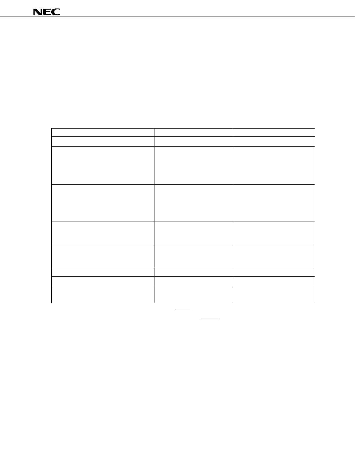
Table 1-1. Differences between
Item
Internal ROM structure Flash memory Mask ROM
Internal ROM capacity 60 Kbytes
Internal expansion RAM capacity 1024 bytes
Internal ROM capacity changeable/not Changeable
changeable with memory size switching
register (IMS)
Internal expansion RAM capacity Changeable
changeable/not changeable with internal
expansion RAM size switching register (IXS)
IC pin Not provided Provided
VPP pin Provided Not provided
P60 to P63 pin mask option with internal Not provided Provided
pull-up resistors
µ
µ
PD78F0058Y and Mask ROM Versions
PD78F0058Y Mask ROM Versions
µ
PD780053Y : 24 Kbytes
µ
PD780054Y : 32 Kbytes
µ
PD780055Y : 40 Kbytes
µ
PD780056Y : 48 Kbytes
µ
PD780058Y : 60 Kbytes
µ
PD780053Y : None
µ
PD780054Y : None
µ
PD780055Y : None
µ
PD780056Y : None
µ
PD780058Y : 1024 bytes
Note 1
Note 2
Not changeable
Not changeable
Notes 1. Flash memory is set to 60 Kbytes by RESET input
2. Internal expansion RAM is set to 1024 bytes by RESET input.
Caution The noise resistance and noise radiation differ between flash memory versions and mask
ROM versions. When considering the replacement of flash memory versions with mask ROM
versions in the process from trial manufacturing to mass production, adequate evaluation
should be carried out using CS products (not ES products) of mask ROM versions.
µ
Remark Only the
PD780058Y and 78F0058Y are provided with IXS.
9
Page 10
µ
PD78F0058Y
2. PIN FUNCTIONS
2.1 Port Pins (1/2)
Pin Name I/O Funciton After Reset Alternate Function
P00
P01
P02
P03
P04
P05
Note 1
P07
P10 to P17
P20
P21
P22
P23
P24
P25
P26
P27
P30
P31
P32
P33
P34
P35
P36
P37
Input
I/O
Input
I/O
I/O
I/O
Port 0
7-bit input/output port
Port 1
8-bit input/output port
Input/output can be specified bit-wise.
When used as an input port, an internal pull-up resistor can be
connected by software.
Port 2
8-bit input/output port
Input/output can be specified bit-wise.
When used as an input port, an internal pull-up resistor can be
connected by software.
Port 3
8-bit input/output port
Input/output can be specified bit-wise.
When used as an input port, an internal pull-up resistor can be
connected by software.
Input only
Input/output can be specified bit-wise.
When used as an input port, an internal
pull-up resistor can be connected by
software.
Input only
Note 2
Input
Input
Input
Input
Input
Input
INTP0/TI00
INTP1/TI01
INTP2
INTP3
INTP4
INTP5
XT1
ANI0 to ANI7
SI1
SO1
SCK1
STB/TxD1
BUSY/RxD1
SI0/SB0/SDA0
SO0/SB1/SDA1
SCK0/SCL
TO0
TO1
TO2
TI1
TI2
PCL
BUZ
–
Notes 1. When using P07/XT1 pin as an input port, set 1 to the bit 6 (FRC) of the processor clock control
register (PCC). Do not use the feedback resistor of the subsystem clock oscillator.
2. When using P10/ANI0 to P17/ANI7 pins as analog inputs of A/D converter, the internal pull-up
resistor is automatically set unused.
10
Page 11
µ
PD78F0058Y
2.1 Port Pins (2/2)
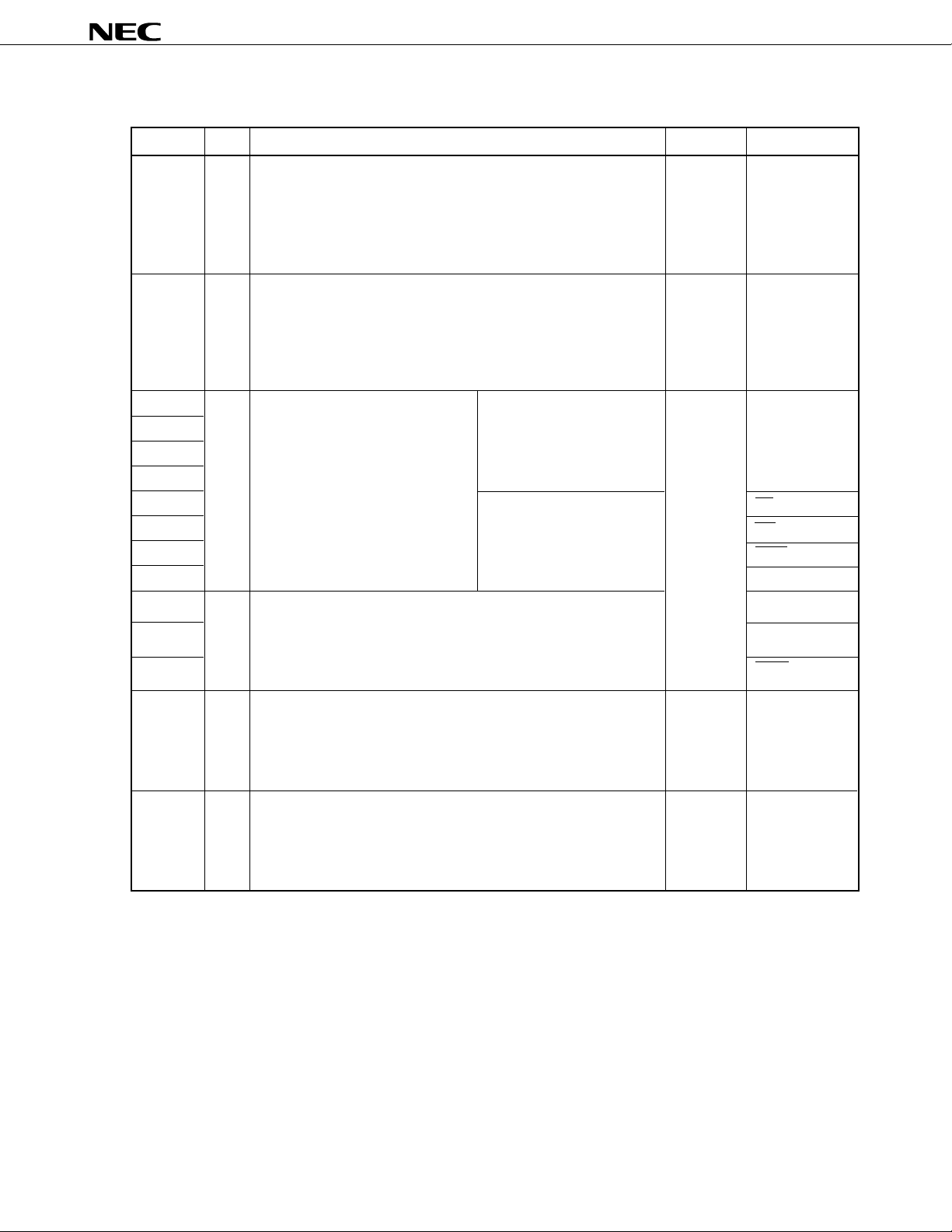
Pin Name I/O Funciton After Reset Alternate Function
P40 to P47
P50 to P57
P60
P61
P62
P63
P64
P65
P66
P67
P70
P71
P72
P120 to P127
P130, P131
I/O
I/O
I/O
I/O
I/O
I/O
Port 4
8-bit input/output port
Input/output can be specified in 8-bit units.
When used as an input port, an internal pull-up resistor can be
connected by software.
Test input flag (KRIF) is set to 1 by the falling edge detection.
Port 5
8-bit input/output port
LED can be driven directly.
Input/output can be specified bit-wise.
When used as an input port, an internal pull-up resistor can be
connected by software.
Port 6
8-bit input/output port
Input/output can be specified bit-wise.
Port 7
3-bit input/output port
Input/output can be specified bit-wise.
When used as an input port, an internal pull-up resistor can be
connected by software.
Port 12
8-bit input/output port
Input/output can be specified bit-wise.
When used as an input port, an internal pull-up resistor can be
connected by software.
Port 13
2-bit input/output port
Input/output can be specified bit-wise.
When used as an input port, an internal pull-up resistor can be
connected by software.
N-ch open drain input/output
port. LED can be driven
directly.
When used as an input port,
an internal pull-up resistor can
be connected by software.
Input
Input
Input
Input
Input
AD0 to AD7
A8 to A15
–
RD
WR
WAIT
ASTB
SI2/RxD0
SO2/TxD0
SCK2/ASCK
RTP0 to RTP7
ANO0, ANO1
11
Page 12

µ
PD78F0058Y
2.2 Non-Port Pins (1/2)
Pin Name I/O Funciton After Reset Alternate Function
INTP0
INTP1
INTP2
INTP3
INTP4
INTP5
SI0
SI1
SI2
SO0
SO1
SO2
SB0
SB1
SDA0
SDA1
SCK0
SCK1
SCK2
SCL
STB
BUSY
RxD0
RxD1
TxD0
TxD1
ASCK
TI00
TI01
TI1
TI2
TO0
TO1
TO2
PCL
BUZ
RTP0 to RTP7
AD0 to AD7
A8 to A15
RD
Input
Input
Output
I/O
I/O
Output
Input
Input
Output
Input
Input
Output
Output
Output
Output
I/O
Output
Output
External interrupt request input by which the effective edge (rising
edge, falling edge, or both rising edge and falling edge) can be
specified
Serial interface serial data input
Serial interface serial data output
Serial interface serial data input/output
Serial interface serial clock input/output
Strobe output for serial interface automatic transmission/reception
Busy input for serial interface automatic transmission/reception
Serial data input for asynchronous serial interface
Serial data output for asynchronous serial interface
Serial clock input for asynchronous serial interface
External count clock input to 16-bit timer (TM0)
Capture trigger signal input to capture register (CR00)
External count clock input to 8-bit timer (TM1)
External count clock input to 8-bit timer (TM2)
16-bit timer output (shared with 14-bit PWM output)
8-bit timer output
Clock output (for trimming of main system clock and subsystem clock)
Buzzer output
Real-time output port to output data in synchronization with triggers
Lower address/data bus for extending memory externally
Higher address bus for extending memory externally
Strobe signal output for read operation of external memory
Input
Input
Input
Input
Input
Input
Input
Input
Input
Input
Input
Input
Input
Input
Input
Input
Input
Input
P00/TI00
P01/TI01
P02
P03
P04
P05
P25/SB0/SDA0
P20
P70/RxD
P26/SB1/SDA1
P21
P71/TxD
P25/SI0/SDA0
P26/SO0/SDA1
S25/SI0/SB0
S26/SO0/SB1
P27/SCL
P22
P72/ASCK
P27/SCK0
P23/TxD1
P24/RxD1
P70/SI2
P24/BUSY
P71/SO2
P23/STB
P72/SCK2
P00/INTP0
P01/INTP1
P33
P34
P30
P31
P32
P35
P36
P120 to P127
P40 to P47
P50 to P57
P64
12
Page 13

µ
PD78F0058Y
2.2 Non-Port Pins (2/2)
Pin Name I/O Funciton After Reset Alternate Function
WR
WAIT
ASTB
ANI0 to ANI7
ANO0, ANO1
AVREF0
AVREF1
AVSS
RESET
X1
X2
XT1
XT2
VDD0
VSS0
VDD1
VSS1
VPP
Output
Input
Output
Input
Output
Input
Input
–
Input
Input
–
Input
–
–
–
–
–
–
Strobe signal output for write operation of external memory
Inserting wait for accessing external memory
Strobe output which externally latches address information output to
port 4 and port 5 to access external memory
A/D converter analog input
D/A converter analog output
A/D converter reference voltage input (shared with analog power
supply)
D/A converter reference voltage input
A/D converter, D/A converter ground potential, Voltage equal to V
System reset input
Connecting crystal resonator for main system clock oscillation
Connecting crystal resonator for subsystem clock oscillation
Positive power supply voltage for ports
Ground potential of ports
Positive power supply (except ports and analog parts)
Ground potential (except ports and analog parts)
Applying high-voltage for program write/verify
Connected directly to VSS0 in normal operation mode
SS0
Input
Input
Input
Input
Input
–
–
–
–
–
–
Input
–
–
–
–
–
–
P65
P66
P67
P10 to P17
P130, P131
–
–
–
–
–
–
P07
–
–
–
–
–
–
13
Page 14

2.3 Pin I/O Circuits and Recommended Connection of Unused Pins
Table 2-1 shows the I/O circuit type of each pin and the recommended connection of unused pins.
For the configuration of each I/O circuit type, refer to Figure 2-1.
Table 2-1. I/O Circuit Type of Each Pin (1/2)
Pin Name I/O Circuit Type I/O Recommended Connection when Not Used
P00/INTP0/TI00
P01/INTP1/TI01
P02/INTP2
P03/INTP3
P04/INTP4
P05/INTP5
P07/XT1
P10/ANI0 to P17/ANI7
P20/SI1
P21/SO1
P22/SCK1
P23/STB/TxD1
P24/BUSY/RxD1
P25/SI0/SB0/SDA0
P26/SO0/SB1/SDA1
P27/SCK0/SCL
P30/TO0
P31/TO1
P32/TO2
P33/TI1
P34/TI2
P35/PCL
P36/BUZ
P37
P40/AD0 to P47/AD7
P50/A8 to P57/A15
P60 to P63
P64/RD
P65/WR
P66/WAIT
P67/ASTB
P70/SI2/RxD0
P71/SO2/TxD0
P72/SCK2/ASCK
P120/RTP0 to P127/RTP7
P130/ANO0, P131/ANO1
2
8-C
16
11-D
8-C
5-H
8-C
5-H
8-C
10-B
5-H
8-C
5-H
5-N
5-H
13-K
5-H
8-C
5-H
8-C
5-H
12-C
Input
I/O
Input
I/O
Connected to VSS0.
Independently connected to VSS0 through a resistor.
Connected to VDD0.
Independently connected to VDD0 or VSS0 through a resistor.
Independently connected to VDD0 through a resistor.
Independently connected to VDD0 or VSS0 through a resistor.
Independently connected to VDD0 through a resistor.
Independently connected to VDD0 or VSS0 through a resistor.
Independently connected to VSS0 through a resistor.
µ
PD78F0058Y
14
Page 15

µ
PD78F0058Y
Table 2-1. I/O Circuit Type of Each Pin (2/2)
Pin Name I/O Circuit Type I/O Recommended Connection when Not Used
RESET
XT2
AV
REF0
AVREF1
AVSS
VPP
2
16
–
Input––
Open
Connected to VSS0.
Connected to VDD0.
Connected to VSS0.
Connected directly to VSS0.
15
Page 16

Figure 2-1. List of Pin I/O Circuits (1/2)
µ
PD78F0058Y
Type 2
IN
Schmitt trigger input with hysteresis characteristics
Type 5-H
pullup
enable
V
DD0
P-ch
VDD0
data
output
disable
P-ch
N-ch
VSS0
input
enable
IN/OUT
Type 8-C
pullup
enable
data
output
disable
Type 10-B
pullup
enable
data
open drain
output disable
VDD0
P-ch
DD0
V
P-ch
IN/OUT
N-ch
V
SS0
V
DD0
P-ch
VDD0
P-ch
IN/OUT
N-ch
VSS0
Type 5-N
pullup
enable
data
output
disable
VDD0
P-ch
N-ch
VSS0
V
V
DD0
Type 11-D
pullup
enable
P-ch
data
VDD0
P-ch
DD0
P-ch
IN/OUT
IN/OUT
output
disable
Comparator
P-ch
+
–
VSS0
N-ch
VSS0
N-ch
VREF (threshold voltage)
input
enable
16
Page 17

Figure 2-1. List of Pin I/O Circuits (2/2)
µ
PD78F0058Y
Type 12-C
pullup
enable
data
output
disable
input
enable
Analog output voltage
Type 13-K
data
output disable
RD
VDD0
P-ch
N-ch
VSS0
P-ch
N-ch
VDD0
VSS0
VSS0
N-ch
P-ch
V
P-ch
DD0
IN/OUT
IN/OUT
Type 16
feedback
cut-off
P-ch
XT1 XT2
Medium breakdown input buffer
17
Page 18

µ
PD78F0058Y
3. MEMORY SIZE SWITCHING REGISTER (IMS)
This register sets a part of internal memory unused by software. The memory map can be made the same as
that of mask ROM versions with different types of internal memory (ROM and RAM) by setting the memory size
switching register (IMS).
The IMS is set with an 8-bit memory manipulation instruction.
RESET input sets the IMS to CFH.
Figure 3-1. Format of Memory Size Switching Register
Symbol
RAM27RAM16RAM0504ROM33ROM22ROM11ROM0
IMS
0
Address
FFF0H
ROM3
0
1
1
1
1
1
Others
RAM21RAM11RAM00Selection of Internal High-speed RAM Capacity
Others
ROM2
1
0
0
1
1
1
After reset
CFH
ROM1
1
0
1
0
1
1
R/W
R/W
ROM0
Selection of Internal ROM Capacity
0
24 Kbytes
0
32 Kbytes
0
40 Kbytes
0
48 Kbytes
0
56 Kbytes
1
60 Kbytes
Setting prohibited
1024 bytes
Setting prohibited
Note
Note When using external device expansion function, set the internal ROM capacity to less than 56
Kbytes.
Table 3-1 shows the IMS set value to make the memory mapping the same as those of mask ROM versions.
Table 3-1. Set Value of Memory Size Switching Register
Target Mask ROM Versions IMS Set Value
µ
PD780053Y C6H
µ
PD780054Y C8H
µ
PD780055Y CAH
µ
PD780056Y CCH
µ
PD780058Y CFH
18
Page 19

µ
PD78F0058Y
4. INTERNAL EXPANSION RAM SIZE SWITCHING REGISTER (IXS)
This register sets the internal expansion RAM capacity by software. The memory map can be made the same
as that of mask ROM versions with different types of internal expansion RAM by setting the internal expansion
RAM size switching register (IXS).
The IXS is set with an 8-bit memory manipulation instruction.
RESET input sets the IXS to 0AH.
Figure 4-1. Format of Internal Expansion RAM Size Switching Register
Symbol
IXS
7
6
5
0
0
0
04IXRAM33IXRAM22IXRAM11IXRAM0
0
Address
FFF4H
IXRAM3
1
1
Others
After resetWR/W
0AH
IXRAM2
IXRAM1
1
0
0
1
IXRAM0
Selection of Internal Expansion RAM Capacity
0
0 bytes
0
1024 bytes
Setting prohibited
Table 4-1 shows the IXS set value to make the memory mapping the same as those of mask ROM versions.
Table 4-1. Set Value of Internal Expansion RAM Size Switching Register
Target Mask ROM Versions IXS Set Value
µ
PD780053Y 0CH
µ
PD780054Y
µ
PD780055Y
µ
PD780056Y
µ
PD780058Y 0AH
Remark Even if a µPD78F0058Y program in which MOV IXS, #0CH is written is executed on the µPD780055Y
and 780056Y, the operation will not be affected.
19
Page 20

µ
PD78F0058Y
5. FLASH MEMORY PROGRAMMING
Writing to a flash memory can be performed without removing the memory from the target system (on-board).
Writing is performed connecting the dedicated flash programmer (Flashpro II) to the host machine and the target
system.
Remark Flashpro II is a product of Naitou Densei Machidaseisakusho Co., Ltd.
5.1 Selection of Transmission Method
Writing to a flash memory is performed using the Flashpro II with a serial transmission mode. One of the
transmission method is selected from those in Table 5-1. The selection of the transmission method is made by
using the format shown in Figure 5-1. Each transmission method is selected by the number of V
in Table 5-1.
Table 5-1. List of Transmission Method
Transmission Method Channels Pin VPP Pulses
3-wired serial I/O 3 P27/SCK0/SCL 0
P26/SO0/SB1/SDA1
P25/SI0/SB0/SDA0
P22/SCK1 1
P21/SO1
P20/SI1
P72/SCK2/ASCK 2
P71/SO2/TxD0
P70/SI1/RxD0
I2C bus 2 P27/SCK0/SCL 4
P25/SI0/SB0/SDA0
P27/SCK0/SCL 5
P26/SO0/SB1/SDA1
UART 2 P71/SO2/TxD0 8
P70/SI2/RxD0
P23/TxD1 9
P24/RxD1
Pseudo 3-wired serial I/O
Note
1 P32/TO2 (serial clock input/output) 12
P31/TO1 (serial data output)
P30/TO0 (serial data input)
PP pulses shown
20
Note Serial transmission is performed by controlling the port using software.
Caution Select a communication system always using the number of V
PP pulses shown in Table
5-1.
Page 21

µ
PD78F0058Y
Figure 5-1. Format of Transmission Method Selection
10 V
V
PP
DD
RESET
V
V
SS
V
DD
V
SS
12 n
5.2 Function of Flash Memory Programming
Operations such as writing to a flash memory are performed by various command/data transmission and
reception operations according to the selected transmission method. Table 5-2 shows major functions of flash
memory programming.
Table 5-2. Major Functions of Flash Memory Programming
Functions Descriptions
Reset
Batch verify
Block verify
Batch delete
Block delete
Convergence
Batch blank check
Block blank check
High-speed write
Continuous write
Status
Oscillation frequency setting
Delete time setting
Baud rate setting
Convergence time setting
Silicon signature read
Used to stop write operation and detect transmission cycle.
Compares the entire memory contents with the input data.
Compares the contents of the specified memory blocks with the input data.
Deletes the entire memory contents.
Deletes the contents of the specified memory block, setting 16 Kbytes as one memory
block.
Prevents over-deletion.
Checks the deletion status of the entire memory.
Checks the deletion status of the specified block.
Performs write to the flash memory based on the write start address and the number of
data to be written (number of bytes).
Performs continuous write based on the information input with high-speed write
operation.
Used to confirm the current operating mode and operation end.
Sets the frequency of the resonator.
Sets the memory delete time.
Sets the transmission rate in transmission using UART system.
Sets the correction time in convergence.
Outputs the device name and memory capacity, and device block information.
21
Page 22

µ
PD78F0058Y
5.3 Connection of Flashpro II
The connection of the Flashpro II and the µPD78F0058Y differs according to the transmission method. The
connection for each transmission method is shown in Figures 5-2 to 5-4.
Figure 5-2. Connection of Flashpro II for 3-wired Serial I/O System
Flashpro II
VPP
VDD
RESET
SCK
SO
SI
GND
n = 0 to 2
Figure 5-3. Connection of Flashpro II for I
Flashpro II
V
PP
V
DD
RESET
µ
PD78F0058Y
PP
V
VDD
RESET
SCKn
SIn
SOn
SS
V
2
C bus System
µ
PD78F0058Y
V
PP
V
DD
RESET
SCL
SDA
GND
SCL
SDAn
V
SS
n = 0, 1
Figure 5-4. Connection of Flashpro II for UART System
Flashpro II
VPP
VDD
RESET
TxD
RxD
GND
n = 0, 1
µ
PD78F0058Y
PP
V
VDD
RESET
RxDn
TxDn
SS
V
22
Page 23

µ
PD78F0058Y
Figure 5-5. Connection of Flashpro II for Pseudo 3-wired Serial I/O System
Flashpro II
RESET
VPP
VDD
SCK
SO
GND
µ
PD78F0058Y
PP
V
VDD
RESET
P32 (serial clock)
P30 (serial input)
SI
P31 (serial output)
SS
V
23
Page 24

6. PACKAGE DRAWINGS
80-pin plastic QFP (14 × 14) (Unit: mm)
80 PIN PLASTIC QFP (14×14)
µ
PD78F0058Y
A
B
61
60
41
40
CD
80
1
20
21
F
G
M
I
H
P
J
K
N
L
NOTE
Each lead centerline is located within 0.13 mm (0.005 inch) of
its true position (T.P.) at maximum material condition.
detail of lead end
S
Q
R
M
ITEM MILLIMETERS INCHES
A 17.2±0.4 0.677±0.016
B 14.0±0.2 0.551
C 14.0±0.2 0.551
D 17.2±0.4 0.677±0.016
F 0.825 0.032
G 0.825 0.032
H 0.30±0.10 0.012
I 0.13 0.005
J 0.65 (T.P.) 0.026 (T.P.)
K 1.6±0.2 0.063±0.008
L 0.8±0.2 0.031
M 0.15 0.006
N 0.10 0.004
P 2.7 0.106
Q 0.1±0.1 0.004±0.004
R5°±5° 5°±5°
S 3.0 MAX. 0.119 MAX.
+0.10
–0.05
+0.009
–0.008
+0.009
–0.008
+0.004
–0.005
+0.009
–0.008
+0.004
–0.003
S80GC-65-3B9-4
24
Page 25

80-pin plastic QFP (14 × 14) (Unit: mm)
80 PIN PLASTIC QFP (14×14)
µ
PD78F0058Y
A
B
4160
4061
detail of lead end
2180
201
F
G
H
M
I
P
N
NOTE
Each lead centerline is located within 0.13 mm (0.005 inch) of
its true position (T.P.) at maximum material condition.
C D
S
R
Q
J
K
M
L
ITEM MILLIMETERS INCHES
A 17.20±0.20 0.677±0.008
+0.009
B 14.00±0.20 0.551
C 14.00±0.20 0.551
D 17.20±0.20 0.677±0.008
F 0.825 0.032
G 0.825 0.032
H 0.32±0.06 0.013
I 0.13 0.005
J 0.65 (T.P.) 0.026 (T.P.)
K 1.60±0.20 0.063±0.008
L 0.80±0.20 0.031
+7°
–3°
+0.03
–0.07
M 0.17 0.007
N 0.10 0.004
P 1.40±0.10 0.055±0.004
Q 0.125±0.075 0.005±0.003
R3° 3°
S 1.70 MAX. 0.067 MAX.
+0.009
–0.008
–0.008
+0.009
–0.008
+0.002
–0.003
+0.009
–0.008
+0.001
–0.003
+7°
–3°
P80GC-65-8BT
25
Page 26

80-pin plastic TQFP (fine pitch) (12 × 12) (Unit: mm)
80 PIN PLASTIC TQFP (FINE PITCH) ( 12)
A
B
µ
PD78F0058Y
60
61
F
80
1
G
H
M
I
41
40
21
20
J
K
P
N
L
NOTE
Each lead centerline is located within 0.10 mm (0.004 inch) of
its true position (T.P.) at maximum material condition.
detail of lead end
C
S
D
Q
R
M
ITEM MILLIMETERS INCHES
A 14.0±0.2 0.551
B 12.0±0.2 0.472
C 12.0±0.2 0.472
D 14.0±0.2 0.551
F
1.25
G 1.25
0.10
+0.05
–0.04
+0.055
–0.045
H 0.22 0.009±0.002
I
J 0.5 (T.P.)
K 1.0±0.2 0.039
L 0.5±0.2 0.020
M 0.145 0.006±0.002
N 0.10 0.004
P 1.05 0.041
Q 0.05±0.05
R 5°±5° 5°±5°
S 1.27 MAX. 0.050 MAX.
+0.009
–0.008
+0.009
–0.008
+0.009
–0.008
+0.009
–0.008
0.049
0.049
0.004
0.020 (T.P.)
+0.009
–0.008
+0.008
–0.009
0.002±0.002
P80GK-50-BE9-4
26
Page 27

µ
APPENDIX A. DEVELOPMENT TOOLS
The following development tools are available for system development using the µPD78F0058Y.
Language Processing Software
PD78F0058Y
RA78K/0
CC78K/0
DF780058
CC78K/0-L
Notes 1, 2, 3, 4
Notes 1, 2, 3, 4
Notes 1, 2, 3, 4, 8
Notes 1, 2, 3, 4
78K/0 Series common assembler package
78K/0 Series common C compiler package
µ
PD780058 Subseries common device file
78K/0 Series common C compiler library source file
Flash Memory Writing Tools
Flashpro II (FL-PR2) Dedicated flash programmer
Product of Naitou Densei Machidaseisakusho Co., Ltd.
FA-80GC
FA-80GK
Note 8
Note 8
Adapter for flash memory writing
Product of Naitou Densei Machidaseisakusho Co., Ltd.
Debugging Tool
IE-78000-R 78K/0 Series common in-circuit emulator
IE-78000-R-A 78K/0 Series common in-circuit emulator (for integrated debugger)
IE-78000-R-BK 78K/0 Series common brake board
IE-780308-R-EM
EP-78230GC-R
EV-9200GC-80 Socket to be mounted on a target system board made for the 80-pin plastic QFP (GC-3B9,
EP-78054GK-R
TGK-080SDW Adapter to be mounted on a target system board made for the 80-pin plastic QFP (GK-BE9
SM78K0
ID78K0
SD78K/0
DF780058
Notes 5, 6, 7
Notes 4, 5, 6, 7
Notes 1, 2
Notes 1, 2, 3, 4, 5, 6, 7, 8
µ
PD780308 Subseries common emulation board
µ
PD78234 Subseries common emulation probe
GC-8BT type)
µ
PD78054 Subseries common emulation probe
type)
Product of TOKYO ELETECH Corporation
Consult NEC sole agent for purchase.
78K/0 Series common system simulator
Integrated debugger for IE-78000-R-A
Screen debugger for IE-78000-R
µ
PD780058 Subseries common device file
Notes 1. PC-9800 Series (MS-DOSTM) based
TM
2. IBM PC/AT
3. HP9000 Series 300
4. HP9000 Series 700
and compatibles (PC DOSTM/IBM DOSTM/MS-DOS) based
TM
(HP-UXTM) based
TM
(HP-UX) based, SPARCstationTM (SunOSTM) based, EWS4800 Series
(EWS-UX/V) based
5. PC-9800 Series (MS-DOS + Windows
6. IBM PC/AT and compatibles (PC-DOS/IBM DOS/MS-DOS + Windows) based
TM
7. NEWS
(NEWS-OSTM) based
8. Under development
TM
) based
27
Page 28

Real-time OS
µ
PD78F0058Y
RX78K/0
MX78K0
Notes 1, 2, 3, 4
Notes 1, 2, 3, 4
78K/0 Series Real-time OS
78K/0 Series OS
Fuzzy Inference Development Support System
FE9000
FT9080
FI78K
FD78K0
Note 1
Note 1
Notes 1, 2
Notes 1, 2
/FE9200
/FT9085
Note 5
Note 2
Fuzzy knowledge data creation tool
Translator
Fuzzy inference module
Fuzzy inference debugger
Notes 1. PC-9800 Series (MS-DOS) based
2. IBM PC/AT and compatibles (PC DOS/IBM DOS/MS-DOS) based
3. HP9000 Series 300 (HP-UX) based
4. HP9000 Series 700 (HP-UX) based, SPARCstation (SunOS) based, EWS4800 Series (EWS-UX/V)
based
5. IBM PC/AT and compatibles (PC DOS/IBM DOS/MS-DOS + Windows) based
Remarks 1. For third party development tools, refer to the 78K/0 Series Selection Guide (U11126E)
2. The RA78K/0, CC78K/0, SM78K0, ID78K0, SD78K/0, and RX78K/0 are used in combination with
the DF780058.
28
Page 29

APPENDIX B. RELATED DOCUMENTS
Device Related Documents
µ
PD78F0058Y
Document Name
µ
PD780058, 780058Y Subseries User’s Manual U12013J Planned
µ
PD780053, 780054, 780055, 780056, 780058 Preliminary Product Information U12182J Planned
µ
PD78F0058 Preliminary Product Information U12092J Planned
µ
PD780053Y, 780054Y, 780055Y, 780056Y, 780058Y Preliminary Product Information U12328J Planned
µ
PD78F0058Y Preliminary Product Information U12092J This manual
78K/0 Series User’s Manual Instruction U12326J U12326E
78K/0 Series Instruction Table U10903J U10182E
78K/0 Series Instruction Set U10904J –
78 K/0 Series Application Note Fundamental (III) IEA-767 U10182E
Floating-Point Arithmetic Programs
Document No.
Japanese English
IEA-718 IEA-1289
Development Tools Documents (User’s Manual) (1/2)
Document Name
RA78K Series Assembler Package Operation EEU-809 EEU-1399
Language EEU-815 EEU-1404
RA78K Series Structured Assembler Preprocessor EEU-817 EEU-1402
RA78K0 Assembler Package Operation U11802J U11802E
Assembly Language U11801J U11801E
Structured Assembly Language
CC78K Series C Compiler Operation EEU-656 EEU-1280
Language EEU-655 EEU-1284
CC78K0 C Compiler Operation U11517J U11517E
Language U11518J U11518E
CC78K/0 C Compiler Application Note Programming Know-how EEA-618 EEA-1208
CC78K Series Library Source File U12322J –
IE-78000-R EEU-810 U11376E
IE-78000-R-A U10057J U10057E
IE-78000-R-BK EEU-867 EEU-1427
IE-780308-R-EM U11362J U11362E
EP-78230 EEU-985 EEU-1515
EP-78054GK-R EEU-932 EEU1468
SM78K0 System Simulator Windows based Reference U10181J U10181E
SM78K Series System Simulator External Parts User Open U10092J U10092E
Interface Specification
Document No.
Japanese English
U11789J U11789E
Caution The contents of the above related documents are subject to change without notice. The latest
documents should be used for design, etc.
29
Page 30

Development Tools Documents (User’s Manual) (2/2)
µ
PD78F0058Y
Document Name
ID78K0 Integrated Debugger EWS based Reference U11151J –
ID78K0 Integrated Debugger PC based Reference U11539J U11539E
ID78K0 Integrated Debugger Windows based Guide U11649J U11649E
SD78K0 Screen Debugger Introduction EEU-852 U10539E
PC-9800 Series (MS-DOS) based Reference U10952J –
SD78K/0 Screen Debugger Guide EEU-5024 EEU-1414
IBM PC/AT (PC DOS) based Reference U11279J U11279E
Document No.
Japanese English
Embedded Software Documents (User’s Manual)
Document Name
78K/0 Series Real-time OS Fundamental U11537J U15137E
Installation U11536J U15136E
OS for 78K/0 Series MX78K0 Fundamental U12257J –
Fuzzy Knowledge Data Creation Tool EEU-829 EEU-1438
78K/0, 78K/II, 87AD Series Fuzzy Inference Development Support System Translator EEU-862 EEU-1444
78K/0 Series Fuzzy Inference Development Support System Fuzzy Inference Module EEU-858 EEU-1441
78K/0 Series Fuzzy Inference Development Support System Fuzzy Inference Debugger EEU-921 EEU-1458
Document No.
Japanese English
Other Documents
Document Name
IC PACKAGE MANUAL C10943X
Semiconductor Device Mounting Technology Manual C10535J C10535E
Quality Grade on NEC Semiconductor Devices C11531J C11531E
Reliable Quality Maintenance on NEC Semiconductor Devices C10983J C10983E
Electrostatic Discharge (ESD) Test MEM-539 –
Semiconductor Devices Quality Guarantee Guide C11893J C11893E
Microcomputer Product Series Guide U11416J –
Document No.
Japanese English
Caution The contents of the above related documents are subject to change without notice. The latest
documents should be used for design, etc.
30
Page 31

[MEMO]
µ
PD78F0058Y
31
Page 32

[MEMO]
µ
PD78F0058Y
32
Page 33

[MEMO]
µ
PD78F0058Y
33
Page 34

NOTES FOR CMOS DEVICES
1 PRECAUTION AGAINST ESD FOR SEMICONDUCTORS
Note: Strong electric field, when exposed to a MOS device, can cause destruction
of the gate oxide and ultimately degrade the device operation. Steps must be
taken to stop generation of static electricity as much as possible, and quickly
dissipate it once, when it has occurred. Environmental control must be
adequate. When it is dry, humidifier should be used. It is recommended to
avoid using insulators that easily build static electricity. Semiconductor
devices must be stored and transported in an anti-static container, static
shielding bag or conductive material. All test and measurement tools including
work bench and floor should be grounded. The operator should be grounded
using wrist strap. Semiconductor devices must not be touched with bare
hands. Similar precautions need to be taken for PW boards with semiconductor
devices on it.
µ
PD78F0058Y
2 HANDLING OF UNUSED INPUT PINS FOR CMOS
Note: No connection for CMOS device inputs can be cause of malfunction. If no
connection is provided to the input pins, it is possible that an internal input
level may be generated due to noise, etc., hence causing malfunction. CMOS
device behave differently than Bipolar or NMOS devices. Input levels of CMOS
devices must be fixed high or low by using a pull-up or pull-down circuitry.
Each unused pin should be connected to VDD or GND with a resistor, if it is
considered to have a possibility of being an output pin. All handling related
to the unused pins must be judged device by device and related specifications
governing the devices.
3 STATUS BEFORE INITIALIZATION OF MOS DEVICES
Note: Power-on does not necessarily define initial status of MOS device. Production
process of MOS does not define the initial operation status of the device.
Immediately after the power source is turned ON, the devices with reset
function have not yet been initialized. Hence, power-on does not guarantee
out-pin levels, I/O settings or contents of registers. Device is not initialized
until the reset signal is received. Reset operation must be executed immediately
after power-on for devices having reset function.
34
Page 35

µ
PD78F0058Y
Regional Information
Some information contained in this document may vary from country to country. Before using any NEC
product in your application, please contact the NEC office in your country to obtain a list of authorized
representatives and distributors. They will verify:
• Device availability
• Ordering information
• Product release schedule
• Availability of related technical literature
• Development environment specifications (for example, specifications for third-party tools and
components, host computers, power plugs, AC supply voltages, and so forth)
• Network requirements
In addition, trademarks, registered trademarks, export restrictions, and other legal issues may also vary
from country to country.
NEC Electronics Inc. (U.S.)
Santa Clara, California
Tel: 800-366-9782
Fax: 800-729-9288
NEC Electronics (Germany) GmbH
Duesseldorf, Germany
Tel: 0211-65 03 02
Fax: 0211-65 03 490
NEC Electronics (UK) Ltd.
Milton Keynes, UK
Tel: 01908-691-133
Fax: 01908-670-290
NEC Electronics Italiana s.r.1.
Milano, Italy
Tel: 02-66 75 41
Fax: 02-66 75 42 99
NEC Electronics (Germany) GmbH
Benelux Office
Eindhoven, The Netherlands
Tel:040-2445845
Fax: 040-2444580
NEC Electronics (France) S.A.
Velizy-Villacoublay, France
Tel:01-30-67 58 00
Fax: 01-30-67 58 99
NEC Electronics (France) S.A.
Spain Office
Madrid, Spain
Tel: 01-504-2787
Fax: 01-504-2860
NEC Electronics (Germany) GmbH
Scandinavia Office
Taeby, Sweden
Tel: 08-63 80 820
Fax: 08-63 80 388
NEC Electronics Hong Kong Ltd.
Hong Kong
Tel:2886-9318
Fax: 2886-9022/9044
NEC Electronics Hong Kong Ltd.
Seoul Branch
Seoul, Korea
Tel: 02-528-0303
Fax: 02-528-4411
NEC Electronics Singapore Pte. Ltd.
United Square, Singapore 1130
Tel:253-8311
Fax: 250-3583
NEC Electronics Taiwan Ltd.
Taipei, Taiwan
Tel: 02-719-2377
Fax: 02-719-5951
NEC do Brasil S.A.
Sao Paulo-SP, Brasil
Tel: 011-889-1680
Fax: 011-889-1689
J96. 8
35
Page 36

µ
PD78F0058Y
2
Purchase of NEC I
these components in an I
C components conveys a license under the Philips I2C Patent Rights to use
2
C system, provided that the system conforms to the I2C Standard
Specification as defined by Philips.
FIP, IEBus, and QTOP are trademarks of NEC Corporation.
MS-DOS and Windows are trademarks of Microsoft Corporation.
IBM DOS, PC/AT, and PC DOS are trademarks of IBM Corporation.
HP9000 Series 300, HP9000 Series 700, and HP-UX are trademarks of Hewlett-Packard Company.
SPARCstation is a trademark of SPARC International, Inc.
SunOS is a trademark of Sun Microsystems, Inc.
NEWS and NEWS-OS are trademarks of Sony Corporation.
The related documents indicated in this publication may include preliminary versions. However, preliminary
versions are not marked as such.
No part of this document may be copied or reproduced in any form or by any means without the prior written
consent of NEC Corporation. NEC Corporation assumes no responsibility for any errors which may appear in this
document.
NEC Corporation does not assume any liability for infringement of patents, copyrights or other intellectual
property rights of third parties by or arising from use of a device described herein or any other liability arising
from use of such device. No license, either express, implied or otherwise, is granted under any patents,
copyrights or other intellectual property rights of NEC Corporation or others.
While NEC Corporation has been making continuous effort to enhance the reliability of its semiconductor devices,
the possibility of defects cannot be eliminated entirely. To minimize risks of damage or injury to persons or
property arising from a defect in an NEC semiconductor device, customers must incorporate sufficient safety
measures in its design, such as redundancy, fire-containment, and anti-failure features.
NEC devices are classified into the following three quality grades:
"Standard", "Special", and "Specific". The Specific quality grade applies only to devices developed based on
a customer designated "quality assurance program" for a specific application. The recommended applications
of a device depend on its quality grade, as indicated below. Customers must check the quality grade of each
device before using it in a particular application.
Standard: Computers, office equipment, communications equipment, test and measurement equipment,
audio and visual equipment, home electronic appliances, machine tools, personal electronic
equipment and industrial robots
Special: Transportation equipment (automobiles, trains, ships, etc.), traffic control systems, anti-disaster
systems, anti-crime systems, safety equipment and medical equipment (not specifically designed
for life support)
Specific: Aircrafts, aerospace equipment, submersible repeaters, nuclear reactor control systems, life
support systems or medical equipment for life support, etc.
The quality grade of NEC devices is "Standard" unless otherwise specified in NEC’s Data Sheets or Data Books.
If customers intend to use NEC devices for applications other than those specified for Standard quality grade,
they should contact an NEC sales representative in advance.
Anti-radioactive design is not implemented in this product.
36
M4 96. 5
 Loading...