

Page 1

查询m789436供应商
User’s Manual
µ
µ
PD789426, 789436, 789446
µµ
789456 Subseries
8-Bit Single-Chip Microcontrollers
PD789425
µµµµ
PD789426
µµµµ
PD789435
µµµµ
PD789436
µµµµ
PD78F9436
µµµµ
PD789445
µµµµ
PD789446
µµµµ
PD789455
µµµµ
PD789456
µµµµ
PD78F9456
µµµµ
Document No. U15075EJ1V0UM00 (1st edition)
Date Published November 2000 N CP(K)
1999
©
Printed in Japan
2000
Page 2

[MEMO]
2
User’s Manual U15075EJ1V0UM00
Page 3

NOTES FOR CMOS DEVICES
1 PRECAUTION AGAINST ESD FOR SEMICONDUCTORS
Note:
Strong electric field, when exposed to a MOS device, can cause destruction of the gate oxide and
ultimately degrade the device operation. Steps must be taken to stop generation of static electricity
as much as possible, and quickly dissipate it once, when it has occurred. Environmental control
must be adequate. When it is dry, humidifier should be used. It is recommended to avoid using
insulators that easily build static electricity. Semiconductor devices must be stored and transported
in an anti-static container, static shielding bag or conductive material. All test and measurement
tools including work bench and floor should be grounded. The operator should be grounded using
wrist strap. Semiconductor devices must not be touched with bare hands. Similar precautions need
to be taken for PW boards with semiconductor devices on it.
2 HANDLING OF UNUSED INPUT PINS FOR CMOS
Note:
No connection for CMOS device inputs can be cause of malfunction. If no connection is provided
to the input pins, it is possible that an internal input level may be generated due to noise, etc., hence
causing malfunction. CMOS devices behave differently than Bipolar or NMOS devices. Input levels
of CMOS devices must be fixed high or low by using a pull-up or pull-down circuitry. Each unused
DD
pin should be connected to V
being an output pin. All handling related to the unused pins must be judged device by device and
related specifications governing the devices.
or GND with a resistor, if it is considered to have a possibility of
3 STATUS BEFORE INITIALIZATION OF MOS DEVICES
Note:
Power-on does not necessarily define initial status of MOS device. Production process of MOS
does not define the initial operation status of the device. Immediately after the power source is
turned ON, the devices with reset function have not yet been initialized. Hence, power-on does
not guarantee out-pin levels, I/O settings or contents of registers. Device is not initialized until the
reset signal is received. Reset operation must be executed immediately after power-on for devices
having reset function.
EEPROM is a trademark of NEC Corporation.
Windows and Windows NT are either registered trademarks or trademarks of Microsoft Corporation in the
United States and/or other countries.
PC/AT is a trademark of International Business Machines Corporation.
HP9000 series 700 and HP-UX are trademarks of Hewlett-Packard Company.
SPARCstation is a trademark of SPARC International, Inc.
Solaris and SunOS are trademarks of Sun Microsystems, Inc.
OSF/Motif is a trademark of Open Software Foundation, Inc.
NEWS and NEWS-OS are trademarks of Sony Corporation.
TRON is an abbreviation of The Realtime Operating system Nucleus.
ITRON is an abbreviation of Industrial TRON.
User’s Manual U15075EJ1V0UM00
3
Page 4

The export of these products from Japan is regulated by the Japanese government. The export of some or all of these
products may be prohibited without governmental license. To export or re-export some or all of these products from a
country other than Japan may also be prohibited without a license from that country. Please call an NEC sales
representative.
License not needed:
The customer must judge the need for license:
PD78F9436, 78F9456
µ
PD789425, 789426, 789435, 789436, 789445,
µ
789446, 789455, 789456
•
The information in this document is current as of September, 2000. The information is subject to
change without notice. For actual design-in, refer to the latest publications of NEC's data sheets or
data books, etc., for the most up-to-date specifications of NEC semiconductor products. Not all
products and/or types are available in every country. Please check with an NEC sales representative
for availability and additional information.
•
No part of this document may be copied or reproduced in any form or by any means without prior
written consent of NEC. NEC assumes no responsibility for any errors that may appear in this document.
•
NEC does not assume any liability for infringement of patents, copyrights or other intellectual property rights of
third parties by or arising from the use of NEC semiconductor products listed in this document or any other
liability arising from the use of such products. No license, express, implied or otherwise, is granted under any
patents, copyrights or other intellectual property rights of NEC or others.
•
Descriptions of circuits, software and other related information in this document are provided for illustrative
purposes in semiconductor product operation and application examples. The incorporation of these
circuits, software and information in the design of customer's equipment shall be done under the full
responsibility of customer. NEC assumes no responsibility for any losses incurred by customers or third
parties arising from the use of these circuits, software and information.
•
While NEC endeavours to enhance the quality, reliability and safety of NEC semiconductor products, customers
agree and acknowledge that the possibility of defects thereof cannot be eliminated entirely. To minimize
risks of damage to property or injury (including death) to persons arising from defects in NEC
semiconductor products, customers must incorporate sufficient safety measures in their design, such as
redundancy, fire-containment, and anti-failure features.
•
NEC semiconductor products are classified into the following three quality grades:
"Standard", "Special" and "Specific". The "Specific" quality grade applies only to semiconductor products
developed based on a customer-designated "quality assurance program" for a specific application. The
recommended applications of a semiconductor product depend on its quality grade, as indicated below.
Customers must check the quality grade of each semiconductor product before using it in a particular
application.
"Standard": Computers, office equipment, communications equipment, test and measurement equipment, audio
and visual equipment, home electronic appliances, machine tools, personal electronic equipment
and industrial robots
"Special": Transportation equipment (automobiles, trains, ships, etc.), traffic control systems, anti-disaster
systems, anti-crime systems, safety equipment and medical equipment (not specifically designed
for life support)
"Specific": Aircraft, aerospace equipment, submersible repeaters, nuclear reactor control systems, life
support systems and medical equipment for life support, etc.
The quality grade of NEC semiconductor products is "Standard" unless otherwise expressly specified in NEC's
data sheets or data books, etc. If customers wish to use NEC semiconductor products in applications not
intended by NEC, they must contact an NEC sales representative in advance to determine NEC's willingness
to support a given application.
(Note)
(1) "NEC" as used in this statement means NEC Corporation and also includes its majority-owned subsidiaries.
(2) "NEC semiconductor products" means any semiconductor product developed or manufactured by or for
NEC (as defined above).
M8E 00.4
4
User’s Manual U15075EJ1V0UM00
Page 5

Regional Information
Some information contained in this document may vary from country to country. Before using any NEC
product in your application, pIease contact the NEC office in your country to obtain a list of authorized
representatives and distributors. They will verify:
•
Device availability
•
Ordering information
•
Product release schedule
•
Availability of related technical literature
•
Development environment specifications (for example, specifications for third-party tools and
components, host computers, power plugs, AC supply voltages, and so forth)
•
Network requirements
In addition, trademarks, registered trademarks, export restrictions, and other legal issues may also vary
from country to country.
NEC Electronics Inc. (U.S.)
Santa Clara, California
Tel: 408-588-6000
800-366-9782
Fax: 408-588-6130
800-729-9288
NEC Electronics (Germany) GmbH
Duesseldorf, Germany
Tel: 0211-65 03 02
Fax: 0211-65 03 490
NEC Electronics (UK) Ltd.
Milton Keynes, UK
Tel: 01908-691-133
Fax: 01908-670-290
NEC Electronics Italiana s.r.l.
Milano, Italy
Tel: 02-66 75 41
Fax: 02-66 75 42 99
NEC Electronics (Germany) GmbH
Benelux Office
Eindhoven, The Netherlands
Tel: 040-2445845
Fax: 040-2444580
NEC Electronics (France) S.A.
Velizy-Villacoublay, France
Tel: 01-30-67 58 00
Fax: 01-30-67 58 99
NEC Electronics (France) S.A.
Madrid Office
Madrid, Spain
Tel: 91-504-2787
Fax: 91-504-2860
NEC Electronics (Germany) GmbH
Scandinavia Office
Taeby, Sweden
Tel: 08-63 80 820
Fax: 08-63 80 388
NEC Electronics Hong Kong Ltd.
Hong Kong
Tel: 2886-9318
Fax: 2886-9022/9044
NEC Electronics Hong Kong Ltd.
Seoul Branch
Seoul, Korea
Tel: 02-528-0303
Fax: 02-528-4411
NEC Electronics Singapore Pte. Ltd.
United Square, Singapore
Tel: 65-253-8311
Fax: 65-250-3583
NEC Electronics Taiwan Ltd.
Taipei, Taiwan
Tel: 02-2719-2377
Fax: 02-2719-5951
NEC do Brasil S.A.
Electron Devices Division
Guarulhos-SP Brasil
Tel: 55-11-6462-6810
Fax: 55-11-6462-6829
User’s Manual U15075EJ1V0UM00
J00.7
5
Page 6

[MEMO]
6
User’s Manual U15075EJ1V0UM00
Page 7

INTRODUCTION
Target Readers
Purpose
Organization
This manual is intended to give user engineers an understanding of the functions of
PD789426, 789436, 789446, and 789456 Subseries to design and develop its
the
µ
application systems and programs.
Target products:
PD789426 Subseries:µPD789425, 789426
•
µ
PD789436 Subseries:µPD789435, 789436
•
µ
PD789446 Subseries:µPD789445, 789446
•
µ
PD789456 Subseries:µPD789455, 789456
•
µ
This manual is designed to deepen your understanding of the following functions
using the following organization.
Two manuals are available for the µPD789426, 789436, 789446, and 789456
Subseries:
This manual and the instruction manual (common to the 78K/0S Series).
PD789426, 789436, 789446,
µ
and 789456 Subseries
User’s Manual
Pin functions
•
Internal block functions
•
Interrupts
•
Other internal peripheral functions
•
78K/0S Series
User’s Manual
Instructions
CPU function
•
Instruction set
•
Instruction description
•
How to Use This Manual
It is assumed that the readers of this manual have general knowledge of electrical
engineering, logic circuits, and microcontrollers.
To understand the overall functions of the
•
789456 Subser ies
Read this manual in the order of the
→
How to read register formats
•
The name of a bit whose number is enclosed in brackets is reserved for the
→
assembler and is defined for the C compiler by the header file sfrbit.h.
To learn the detailed functions of a register whose register name is known
•
See
→
To learn the details of the instruction functions of the 78K/0S series
•
→
APPENDIX C REGISTER INDEX
Refer to
available.
78K/0S Series Instructions User’s Manual (U11047E)
CONTENTS
PD789426, 789436, 789446, and
µ
.
.
separately
User’s Manual U15075EJ1V0UM00 7
Page 8

Conventions
Data significance: Higher digits on the left and lower digits on the right
Active low representation: xxx (overscore over pin or signal name)
: Footnote for item marked with
Note
Caution
Remark
: Information requiring particular attention
: Supplementary information
Note
in the text
Numerical representation: Binary ... xxxx or xxxxB
Decimal ... xxxx
Hexadecimal ... xxxxH
Related Documents
The related documents indicated in this publication may include preliminary versions.
However, preliminary versions are not marked as such.
Documents Related to Devices
Document Name
µ
PD789425, 789426, 789435, 789436, 789445, 789446, 789455, 789456
Preliminary Product I nf orm ation
µ
PD78F9436, 78F9456 Preliminary Product Information To be prepared To be prepared
µ
PD789426, 789436, 789446, 789456 Subseries Us er’ s Manual U15075J This manual
78K/0S Series Inst ructions User’s Manual U11047J U11047E
78K/0, 78K/0S Series Fl as h Memory Write Application Note U14458J U14458E
U14493J U14493E
Document No.
Japanese English
Documents Related to Development Tools (User’s Manuals)
Document Name
RA78K0S Assembler Package
SM78K0S, SM78K0 System Simulator Ver. 2.10 or Later
Windows
SM78K Series System Simulator External P art User Open
ID78K0S-NS Integrated Debugger Windows Based Reference U12901J U12901E
ID78K0-NS, ID78K0S-NS Integrated Debugger Ver. 2.20
or Later Windows Based
IE-78K0S-NS U13549J U13549E
IE-789456-NS-EM1 To be prepared To be prepared
TM
Based
Operation U11622J U11622E
Assembly Language U11599J U11599E
Structured Assembl y
Language
Operation U11816J U11816ECC78K/0S C Compiler
Language U11817J U11817E
Operation U14611J To be prepared
Interface Specifi c ations
Operation U14910J To be prepared
U11623J U11623E
U10092J U10092E
Document No.
Japanese English
Caution The related documents listed above are subject to change without notice. Be sure to use the
latest version of each document for designing.
8 User’s Manual U15075EJ1V0UM00
Page 9
Document Related to Embedded Software (User’s Manual)
Document Name
78K/0S Series OS MX78K 0S Fundamental U12938J U12938E
Document No.
Japanese English
Other Related Documents
Document Name
SEMICONDUCTOR SELECTION GUI DE Products & Packages (CD-ROM) X13769X
Semiconductor Device Mounting Technology Manual C10535J C10535E
Quality Grades on NEC Semic onductor Devices C11531J C11531E
NEC Semiconductor Device Reliability /Quality Control System C10983J C10983E
Guide to Prevent Damage for Semi conductor Devices by El ec trostatic Discharge (E S D) C11892J C11892E
Guide to Microcomputer-Relat ed P roducts by Third Parties U11416J —
Document No.
Japanese English
Caution The related documents listed above are subject to change without notice. Be sure to use the
latest version of each document for designing.
User’s Manual U15075EJ1V0UM00 9
Page 10

[MEMO]
10 User’s Manual U15075EJ1V0UM00
Page 11

CONTENTS
CHAPTER 1 GENERAL...........................................................................................................................25
1.1 Features.......................................................................................................................................25
1.2 Applications................................................................................................................................25
1.3 Ordering Information .................................................................................................................26
1.4 Pin Configuration (Top View)....................................................................................................27
1.4.1 Pin configuration of µPD789426, 789436 Subseries (Top View) ................................................. 27
1.4.2 Pin configuration of
PD789446, 789456 Subseries (Top View) ................................................. 28
µ
1.5 78K/0S Series Lineup.................................................................................................................30
1.6 Block Diagram ............................................................................................................................32
1.6.1 Block diagram of µPD789426, 789436 Subseries........................................................................ 32
1.6.2 Block diagram of
PD789446, 789456 Subseries........................................................................ 33
µ
1.7 Overview of Functions...............................................................................................................34
CHAPTER 2 PIN FUNCTIONS................................................................................................................37
2.1 List of Pin Functions..................................................................................................................37
2.2 Description of Pin Functions ....................................................................................................40
2.2.1 P00 to P03 (Port 0)....................................................................................................................... 40
2.2.2 P10, P11 (Port 1).......................................................................................................................... 40
2.2.3 P20 to P26 (Port 2)....................................................................................................................... 40
2.2.4 P30 to P33 (Port 3)....................................................................................................................... 41
2.2.5 P50 to P53 (Port 5)....................................................................................................................... 41
2.2.6 P60 to P65 (Port 6)....................................................................................................................... 41
2.2.7 P70 to P72 (Port 7)....................................................................................................................... 42
2.2.8 P80, P81 (Port 8).......................................................................................................................... 42
2.2.9 P90 to P97 (Port 9)....................................................................................................................... 42
2.2.10 S0 to S14...................................................................................................................................... 42
2.2.11 COM0 to COM3............................................................................................................................ 42
2.2.12 V
to V
...................................................................................................................................42
LC0
LC2
2.2.13 CAPH, CAPL ................................................................................................................................42
2.2.14 RESET.......................................................................................................................................... 42
2.2.15 X1, X2........................................................................................................................................... 42
2.2.16 XT1, XT2 ...................................................................................................................................... 42
DD
2.2.17 V
2.2.18 V
2.2.19 V
................................................................................................................................................ 43
SS
................................................................................................................................................ 43
PP
(µPD78F9436, 78F9456 only)................................................................................................ 43
2.2.20 IC (mask ROM version only)......................................................................................................... 43
2.3 Pin Input/Output Circuits and Recommended Connection of Unused Pins........................44
CHAPTER 3 CPU ARCHITECTURE.......................................................................................................47
3.1 Memory Space............................................................................................................................47
3.1.1 Internal program memory space................................................................................................... 53
User’s Manual U15075EJ1V0UM00 11
Page 12

3.1.2 Internal data memory (internal high-speed RAM) space..............................................................54
3.1.3 Special function register (SFR) area.............................................................................................54
3.1.4 Data memory addressing..............................................................................................................55
3.2 Processor Registers.................................................................................................................. 61
3.2.1 Control registers ...........................................................................................................................61
3.2.2 General-purpose registers............................................................................................................ 64
3.2.3 Special function registers (SFRs).................................................................................................65
3.3 Instruction Address Addressing.............................................................................................. 68
3.3.1 Relative addressing...................................................................................................................... 68
3.3.2 Immediate addressing ..................................................................................................................69
3.3.3 Table indirect addressing .............................................................................................................70
3.3.4 Register addressing......................................................................................................................70
3.4 Operand Address Addressing.................................................................................................. 71
3.4.1 Direct addressing..........................................................................................................................71
3.4.2 Short direct addressing.................................................................................................................72
3.4.3 Special function register (SFR) addressing..................................................................................73
3.4.4 Register addressing......................................................................................................................74
3.4.5 Register indirect addressing......................................................................................................... 75
3.4.6 Based addressing......................................................................................................................... 76
3.4.7 Stack addressing..........................................................................................................................76
CHAPTER 4 PORT FUNCTIONS........................................................................................................... 77
4.1 Port Functions ........................................................................................................................... 77
4.2 Port Configuration..................................................................................................................... 80
4.2.1 Port 0............................................................................................................................................81
4.2.2 Port 1............................................................................................................................................82
4.2.3 Port 2............................................................................................................................................83
4.2.4 Port 3............................................................................................................................................89
4.2.5 Port 5............................................................................................................................................91
4.2.6 Port 6............................................................................................................................................92
4.2.7 Port 7............................................................................................................................................93
4.2.8 Port 8 (
4.2.9 Port 9 (
PD789426, 789436 Subseries only)...............................................................................94
µ
PD789426, 789436 Subseries only)...............................................................................95
µ
4.3 Registers Controlling Port Function........................................................................................ 96
4.4 Port Function Operation......................................................................................................... 102
4.4.1 Writing to I/O port........................................................................................................................102
4.4.2 Reading from I/O port................................................................................................................. 102
4.4.3 Arithmetic operation of I/O port...................................................................................................102
CHAPTER 5 CLOCK GENERATOR.................................................................................................... 103
5.1 Clock Generator Functions .................................................................................................... 103
5.2 Clock Generator Configuration.............................................................................................. 103
5.3 Registers Controlling Clock Generator................................................................................. 105
5.4 System Clock Oscillators ....................................................................................................... 108
5.4.1 Main system clock oscillator.......................................................................................................108
12 User’s Manual U15075EJ1V0UM00
Page 13

5.4.2 Subsystem clock oscillator.........................................................................................................109
5.4.3 Divider circuit..............................................................................................................................111
5.4.4 When no subsystem clock is used ............................................................................................. 111
5.5 Clock Generator Operation .....................................................................................................112
5.6 Changing Setting of System Clock and CPU Clock..............................................................113
5.6.1 Time required for switching between system clock and CPU clock ........................................... 113
5.6.2 Switching between system clock and CPU clock....................................................................... 114
CHAPTER 6 16-BIT TIMER ..................................................................................................................115
6.1 16-Bit Timer Functions ............................................................................................................115
6.2 16-Bit Timer Configuration......................................................................................................116
6.3 Registers Controlling 16-Bit Timer.........................................................................................119
6.4 16-Bit Timer Operation.............................................................................................................123
6.4.1 Operation as timer interrupt........................................................................................................ 123
6.4.2 Operation as timer output........................................................................................................... 125
6.4.3 Capture operation....................................................................................................................... 126
6.4.4 16-bit timer counter 90 readout .................................................................................................. 127
6.4.5 Buzzer output operation ............................................................................................................. 128
6.5 Notes on Using 16-Bit Timer ...................................................................................................129
CHAPTER 7 8-BIT TIMER ....................................................................................................................131
7.1 8-Bit Timer Functions ..............................................................................................................131
7.2 8-Bit Timer Configuration........................................................................................................132
7.3 Registers Controlling 8-Bit Timer...........................................................................................138
7.4 8-Bit Timer Operation...............................................................................................................143
7.4.1 Operation as 8-bit timer counter................................................................................................. 143
7.4.2 Operation as 16-bit timer counter............................................................................................... 153
7.4.3 Operation as carrier generator ................................................................................................... 160
7.4.4 PWM free-running mode operation (timer 50)............................................................................ 164
7.4.5 Operation as PWM output (timer 60).......................................................................................... 168
7.5 Notes on Using 8-Bit Timer .....................................................................................................170
CHAPTER 8 WATCH TIMER................................................................................................................171
8.1 Watch Timer Functions............................................................................................................171
8.2 Watch Timer Configuration .....................................................................................................172
8.3 Watch Timer Control Register.................................................................................................173
8.4 Watch Timer Operation............................................................................................................174
8.4.1 Operation as watch timer............................................................................................................ 174
8.4.2 Operation as interval timer ......................................................................................................... 174
CHAPTER 9 WATCHDOG TIMER........................................................................................................177
9.1 Watchdog Timer Functions.....................................................................................................177
9.2 Watchdog Timer Configuration...............................................................................................178
9.3 Watchdog Timer Control Registers........................................................................................179
User’s Manual U15075EJ1V0UM00 13
Page 14

9.4 Watchdog Timer Operation .................................................................................................... 181
9.4.1 Operation as watchdog timer......................................................................................................181
9.4.2 Operation as interval timer..........................................................................................................182
CHAPTER 10 8-BIT A/D CONVERTER (
µµµµ
PD789426 AND 789446 SUBSERIES)........................ 183
10.1 8-Bit A/D Converter Functions............................................................................................... 183
10.2 8-Bit A/D Converter Configuration......................................................................................... 183
10.3 8-Bit A/D Converter Control Registers.................................................................................. 186
10.4 8-Bit A/D Converter Operation ............................................................................................... 188
10.4.1 Basic operation of 8-bit A/D converter........................................................................................188
10.4.2 Input voltage and conversion result............................................................................................189
10.4.3 Operation mode of 8-bit A/D converter.......................................................................................191
10.5 Cautions Related to 8-Bit A/D Converter............................................................................... 192
CHAPTER 11 10-BIT A/D CONVERTER (
µµµµ
PD789436 AND 789456 SUBSERIES)...................... 197
11.1 10-Bit A/D Converter Functions............................................................................................. 197
11.2 10-Bit A/D Converter Configuration....................................................................................... 197
11.3 10-Bit A/D Converter Control Registers................................................................................ 200
11.4 10-Bit A/D Converter Operation ............................................................................................. 202
11.4.1 Basic operation of 10-bit A/D converter......................................................................................202
11.4.2 Input voltage and conversion result............................................................................................203
11.4.3 Operation mode of 10-bit A/D converter.....................................................................................205
11.5 Cautions Related to 10-Bit A/D Converter............................................................................. 206
CHAPTER 12 SERIAL INTERFACE 20.............................................................................................. 211
12.1 Serial Interface 20 Functions.................................................................................................. 211
12.2 Serial Interface 20 Configuration ........................................................................................... 211
12.3 Serial Interface 20 Control Registers..................................................................................... 215
12.4 Serial Interface 20 Operation.................................................................................................. 222
12.4.1 Operation stop mode.................................................................................................................. 222
12.4.2 Asynchronous serial interface (UART) mode .............................................................................224
12.4.3 3-wire serial I/O mode.................................................................................................................237
CHAPTER 13 LCD CONTROLLER/DRIVER....................................................................................... 247
13.1 LCD Controller/Driver Functions ........................................................................................... 247
13.2 LCD Controller/Driver Configuration..................................................................................... 247
13.3 Registers Controlling LCD Controller/Driver........................................................................ 249
13.4 Setting LCD Controller/Driver ................................................................................................ 253
13.5 LCD Display Data Memory...................................................................................................... 253
13.6 Common and Segment Signals.............................................................................................. 254
13.7 Display Modes.......................................................................................................................... 256
13.7.1 Three-time slot display example.................................................................................................256
13.7.2 Four-time slot display example...................................................................................................259
14 User’s Manual U15075EJ1V0UM00
Page 15

CHAPTER 14 INTERRUPT FUNCTIONS.............................................................................................263
14.1 Interrupt Function Types.........................................................................................................263
14.2 Interrupt Sources and Configuration .....................................................................................263
14.3 Registers Controlling Interrupt Function...............................................................................266
14.4 Interrupt Servicing Operation .................................................................................................272
14.4.1 Non-maskable interrupt request acknowledgment operation..................................................... 272
14.4.2 Maskable interrupt request acknowledgment operation............................................................. 274
14.4.3 Multiple interrupt servicing..........................................................................................................275
14.4.4 Putting interrupt requests on hold...............................................................................................277
CHAPTER 15 STANDBY FUNCTION ..................................................................................................279
15.1 Standby Function and Configuration.....................................................................................279
15.1.1 Standby function......................................................................................................................... 279
15.1.2 Register controlling standby function.......................................................................................... 280
15.2 Standby Function Operation...................................................................................................281
15.2.1 HALT mode ................................................................................................................................ 281
15.2.2 STOP mode................................................................................................................................ 284
CHAPTER 16 RESET FUNCTION........................................................................................................287
CHAPTER 17
µµµµ
PD78F9436, 78F9456...................................................................................................291
17.1 Flash Memory Programming...................................................................................................292
17.1.1 Selecting communication mode..................................................................................................292
17.1.2 Function of flash memory programming.....................................................................................293
17.1.3 Flashpro III connection example.................................................................................................293
17.1.4 Example of settings for Flashpro III (PG-FP3)............................................................................295
CHAPTER 18 MASK OPTIONS............................................................................................................297
CHAPTER 19 INSTRUCTION SET.......................................................................................................299
19.1 Operation...................................................................................................................................299
19.1.1 Operand identifiers and description methods............................................................................. 299
19.1.2 Description of “Operation” column.............................................................................................. 300
19.1.3 Description of “Flag” column....................................................................................................... 300
19.2 Operation List...........................................................................................................................301
19.3 Instructions Listed by Addressing Type................................................................................306
APPENDIX A DEVELOPMENT TOOLS...............................................................................................309
A.1 Language Processing Software..............................................................................................311
A.2 Flash Memory Writing Tools ...................................................................................................312
A.3 Debugging Tools......................................................................................................................313
A.3.1 Hardware.................................................................................................................................... 313
A.3.2 Software ..................................................................................................................................... 314
User’s Manual U15075EJ1V0UM00 15
Page 16

APPENDIX B EMBEDDED SOFTWARE............................................................................................. 315
APPENDIX C REGISTER INDEX......................................................................................................... 317
C.1 Register Index (Alphabetic Order of Register Name) .......................................................... 317
C.2 Register Index (Alphabetic Order of Register Symbol) ....................................................... 319
16 User’s Manual U15075EJ1V0UM00
Page 17

LIST OF FIGURES (1/5)
Figure No. Title Page
2-1 Pin Input/Output Circuits...............................................................................................................................45
3-1 Memory Map (µPD789425, 789435)............................................................................................................. 47
3-2 Memory Map (µPD789426, 789436)............................................................................................................. 48
3-3 Memory Map (µPD78F9436).........................................................................................................................49
3-4 Memory Map (µPD789445, 789455)............................................................................................................. 50
3-5 Memory Map (µPD789446, 789456)............................................................................................................. 51
3-6 Memory Map (µPD78F9456).........................................................................................................................52
3-7 Data Memory Addressing (µPD789425, 789435) .........................................................................................55
3-8 Data Memory Addressing (µPD789426, 789436) .........................................................................................56
3-9 Data Memory Addressing (µPD78F9436).....................................................................................................57
3-10 Data Memory Addressing (µPD789445, 789455) .........................................................................................58
3-11 Data Memory Addressing (µPD789446, 789456) .........................................................................................59
3-12 Data Memory Addressing (µPD78F9456).....................................................................................................60
3-13 Program Counter Configuration ....................................................................................................................61
3-14 Program Status Word Configuration ............................................................................................................. 61
3-15 Stack Pointer Configuration ..........................................................................................................................63
3-16 Data to Be Saved to Stack Memory.............................................................................................................. 63
3-17 Data to Be Restored from Stack Memory...................................................................................................... 63
3-18 General-Purpose Register Configuration...................................................................................................... 64
4-1 Port Types (µPD789426, 789436 Subseries) ...............................................................................................77
4-2 Port Types (µPD789446, 789456 Subseries) ...............................................................................................78
4-3 Block Diagram of P00 to P03........................................................................................................................81
4-4 Block Diagram of P10 and P11.....................................................................................................................82
4-5 Block Diagram of P20....................................................................................................................................83
4-6 Block Diagram of P21 and P26.....................................................................................................................84
4-7 Block Diagram of P22....................................................................................................................................85
4-8 Block Diagram of P23....................................................................................................................................86
4-9 Block Diagram of P24....................................................................................................................................87
4-10 Block Diagram of P25....................................................................................................................................88
4-11 Block Diagram of P30....................................................................................................................................89
4-12 Block Diagram of P31 to P33........................................................................................................................ 90
4-13 Block Diagram of P50 to P53........................................................................................................................ 91
4-14 Block Diagram of Port 6 ................................................................................................................................92
4-15 Block Diagram of P70 to P72........................................................................................................................ 93
4-16 Block Diagram of P80, P81........................................................................................................................... 94
4-17 Block Diagram of P90 to P97........................................................................................................................ 95
4-18 Format of Port Mode Register.......................................................................................................................97
4-19 Format of Pull-Up Resistor Option Register 0...............................................................................................98
4-20 Format of Pull-Up Resistor Option Register B2............................................................................................. 99
4-21 Format of Pull-Up Resistor Option Register B3............................................................................................. 99
User’s Manual U15075EJ1V0UM00 17
Page 18

LIST OF FIGURES (2/5)
Figure No. Title Page
4-22 Format of Pull-Up Resistor Option Register B7...........................................................................................100
4-23 Format of Pull-Up Resistor Option Register B8...........................................................................................100
4-24 Format of Pull-Up Resistor Option Register B9...........................................................................................101
5-1 Block Diagram of Clock Generator..............................................................................................................104
5-2 Format of Processor Clock Control Register...............................................................................................105
5-3 Format of Suboscillation Mode Register .....................................................................................................106
5-4 Format of Subclock Control Register ..........................................................................................................107
5-5 External Circuit of Main System Clock Oscillator........................................................................................108
5-6 External Circuit of Subsystem Clock Oscillator...........................................................................................109
5-7 Examples of Incorrect Resonator Connection.............................................................................................110
5-8 Switching Between System Clock and CPU Clock......................................................................................114
6-1 Block Diagram of 16-Bit Timer.....................................................................................................................117
6-2 Format of 16-Bit Timer Mode Control Register 90.......................................................................................120
6-3 Format of Buzzer Output Control Register 90.............................................................................................121
6-4 Format of Port Mode Register 2..................................................................................................................122
6-5 Settings of 16-Bit Timer Mode Control Register 90 for Timer Interrupt Operation ......................................123
6-6 Timing of Timer Interrupt Operation............................................................................................................124
6-7 Settings of 16-Bit Timer Mode Control Register 90 for Timer Output Operation.........................................125
6-8 Timer Output Timing....................................................................................................................................125
6-9 Settings of 16-Bit Timer Mode Control Register 90 for Capture Operation.................................................126
6-10 Capture Operation Timing (Both Edges of CPT90 Pin Are Specified) ........................................................126
6-11 16-Bit Timer Counter 90 Readout Timing....................................................................................................127
6-12 Settings of Buzzer Output Control Register 90 for Buzzer Output Operation..............................................128
7-1 Block Diagram of Timer 50..........................................................................................................................133
7-2 Block Diagram of Timer 60..........................................................................................................................134
7-3 Block Diagram of Output Controller (Timer 60)...........................................................................................135
7-4 Format of 8-Bit Timer Mode Control Register 50.........................................................................................139
7-5 Format of 8-Bit Timer Mode Control Register 60.........................................................................................141
7-6 Format of Carrier Generator Output Control Register 60............................................................................142
7-7 Format of Port Mode Register 3..................................................................................................................142
7-8 Timing of Interval Timer Operation with 8-Bit Resolution (Basic Operation)...............................................145
7-9 Timing of Interval Timer Operation with 8-Bit Resolution (When CRn0 Is Set to 00H) ...............................145
7-10 Timing of Interval Timer Operation with 8-Bit Resolution (When CRn0 Is Set to FFH)...............................146
7-11 Timing of Interval Timer Operation with 8-Bit Resolution (When CRn0 Changes from N to M (N < M)) .....146
7-12 Timing of Interval Timer Operation with 8-Bit Resolution (When CRn0 Changes from N to M (N > M)) .....147
7-13 Timing of Interval Timer Operation with 8-Bit Resolution (When Timer 60 Match Signal Is
Selected for Timer 50 Count Clock)............................................................................................................148
7-14 Timing of Operation of External Event Counter with 8-Bit Resolution........................................................150
7-15 Timing of Square-Wave Output with 8-Bit Resolution.................................................................................152
18 User’s Manual U15075EJ1V0UM00
Page 19

LIST OF FIGURES (3/5)
Figure No. Title Page
7-16 Timing of Interval Timer Operation with 16-Bit Resolution..........................................................................155
7-17 Timing of External Event Counter Operation with 16-Bit Resolution...........................................................157
7-18 Timing of Square-Wave Output with 16-Bit Resolution...............................................................................159
7-19 Timing of Carrier Generator Operation (When CR60 = N, CRH60 = M (M > N)) ........................................161
7-20 Timing of Carrier Generator Operation (When CR60 = N, CRH60 = M (M < N),
Phases of Carrier Clock and NRZ60 Are Asynchronous) ...........................................................................162
7-21 Timing of Carrier Generator Operation (When CR60 = CRH60 = N).......................................................... 163
7-22 Operation Timing in PWM Free-Running Mode (When Rising Edge Is Selected) ...................................... 165
7-23 Operation Timing When Overwriting CR50 (When Rising Edge Is Selected).............................................165
7-24 Operation Timing in PWM Free-Running Mode (When Both Edges Are Selected) .................................... 166
7-25 Operation Timing in PWM Free-Running Mode (When Both Edges Are Selected)
(When CR50 Is Overwritten).......................................................................................................................167
7-26 PWM Pulse Generator Mode Timing (Basic Operation)..............................................................................169
7-27 PWM Output Mode Timing (When CR60 and CRH60 Are Overwritten)......................................................169
7-28 Start Timing of 8-Bit Timer Counter............................................................................................................. 170
7-29 Timing of Operation as External Event Counter (8-Bit Resolution)............................................................. 170
8-1 Block Diagram of Watch Timer....................................................................................................................171
8-2 Format of Watch Timer Mode Control Register........................................................................................... 173
8-3 Watch Timer/Interval Timer Operation Timing ............................................................................................175
9-1 Block Diagram of Watchdog Timer..............................................................................................................178
9-2 Format of Watchdog Timer Clock Select Register...................................................................................... 179
9-3 Format of Watchdog Timer Mode Register................................................................................................. 180
10-1 Block Diagram of 8-Bit A/D Converter.........................................................................................................184
10-2 Format of A/D Converter Mode Register 0.................................................................................................. 186
10-3 Format of Analog Input Channel Specification Register 0...........................................................................187
10-4 Basic Operation of 8-Bit A/D Converter....................................................................................................... 189
10-5 Relationship Between Analog Input Voltage and A/D Conversion Result...................................................190
10-6 Software-Started A/D Conversion............................................................................................................... 191
10-7 How to Reduce Current Consumption in Standby Mode.............................................................................192
10-8 Conversion Result Read Timing (If Conversion Result Is Undefined).........................................................193
10-9 Conversion Result Read Timing (If Conversion Result Is Normal) .............................................................193
10-10 Analog Input Pin Treatment......................................................................................................................... 194
10-11 A/D Conversion End Interrupt Request Generation Timing ........................................................................195
10-12 AVDD Pin Handling....................................................................................................................................... 195
11-1 Block Diagram of 10-Bit A/D Converter.......................................................................................................198
11-2 Format of A/D Converter Mode Register 0.................................................................................................. 200
11-3 Format of Analog Input Channel Specification Register 0...........................................................................201
11-4 Basic Operation of 10-Bit A/D Converter..................................................................................................... 203
User’s Manual U15075EJ1V0UM00 19
Page 20

LIST OF FIGURES (4/5)
Figure No. Title Page
11-5 Relationship Between Analog Input Voltage and A/D Conversion Result...................................................204
11-6 Software-Started A/D Conversion ...............................................................................................................205
11-7 How to Reduce Current Consumption in Standby Mode.............................................................................206
11-8 Conversion Result Read Timing (If Conversion Result Is Undefined).........................................................207
11-9 Conversion Result Read Timing (If Conversion Result Is Normal)..............................................................207
11-10 Analog Input Pin Treatment.........................................................................................................................208
11-11 A/D Conversion End Interrupt Request Generation Timing.........................................................................209
11-12 AVDD Pin Handling.......................................................................................................................................209
12-1 Block Diagram of Serial Interface 20...........................................................................................................212
12-2 Block Diagram of Baud Rate Generator 20.................................................................................................213
12-3 Format of Serial Operation Mode Register 20.............................................................................................215
12-4 Format of Asynchronous Serial Interface Mode Register 20.......................................................................216
12-5 Format of Asynchronous Serial Interface Status Register 20 .....................................................................218
12-6 Format of Baud Rate Generator Control Register 20..................................................................................219
12-7 Format of Asynchronous Serial Interface Transmit/Receive Data...............................................................231
12-8 Asynchronous Serial Interface Transmission Completion Interrupt Timing.................................................233
12-9 Asynchronous Serial Interface Reception Completion Interrupt Timing......................................................234
12-10 Receive Error Timing...................................................................................................................................235
12-11 3-Wire Serial I/O Mode Timing....................................................................................................................240
13-1 Block Diagram of LCD Controller/Driver......................................................................................................248
13-2 Format of LCD Display Mode Register 0.....................................................................................................250
13-3 Format of LCD Clock Control Register 0.....................................................................................................251
13-4 Format of LCD Voltage Amplification Control Register 0 ............................................................................252
13-5 Relationship Between LCD Display Data Memory Contents and Segment/Common Outputs
(µPD789446, 789456 Subseries)................................................................................................................253
13-6 Common Signal Waveforms........................................................................................................................255
13-7 Voltages and Phases of Common and Segment Signals............................................................................255
13-8 Three-Time Slot LCD Display Pattern and Electrode Connections.............................................................256
13-9 Example of Connecting Three-Time Slot LCD Panel..................................................................................257
13-10 Three-Time Slot LCD Drive Waveform Examples.......................................................................................258
13-11 Four-Time Slot LCD Display Pattern and Electrode Connections...............................................................259
13-12 Example of Connecting Four-Time Slot LCD Panel....................................................................................260
13-13 Four-Time Slot LCD Drive Waveform Examples.........................................................................................261
14-1 Basic Configuration of Interrupt Function....................................................................................................265
14-2 Format of Interrupt Request Flag Registers................................................................................................267
14-3 Format of Interrupt Mask Flag Registers.................................................................................... .................268
14-4 Format of External Interrupt Mode Register 0.............................................................................................269
14-5 Format of External Interrupt Mode Register 1.............................................................................................270
14-6 Configuration of Program Status Word........................................................................................................270
20 User’s Manual U15075EJ1V0UM00
Page 21

LIST OF FIGURES (5/5)
Figure No. Title Page
14-7 Format of Key Return Mode Register 00.....................................................................................................271
14-8 Block Diagram of Falling Edge Detector .....................................................................................................271
14-9 Flow from Generation of Non-Maskable Interrupt Request to Acknowledgment.........................................273
14-10 Timing of Non-Maskable Interrupt Request Acknowledgment....................................................................273
14-11 Non-Maskable Interrupt Request Acknowledgment....................................................................................273
14-12 Interrupt Request Acknowledgment Program Algorithm .............................................................................274
14-13 Interrupt Request Acknowledgment Timing (Example: MOV A, r) ..............................................................275
14-14 Interrupt Request Acknowledgment Timing (When Interrupt Request Flag Is
Generated in Final Clock Under Execution)................................................................................................275
14-15 Example of Multiple Interrupts .....................................................................................................................276
15-1 Format of Oscillation Stabilization Time Select Register.............................................................................280
15-2 Releasing HALT Mode by Interrupt.............................................................................................................282
15-3 Releasing HALT Mode by RESET Input .....................................................................................................283
15-4 Releasing STOP Mode by Interrupt ............................................................................................................285
15-5 Releasing STOP Mode by RESET Input.....................................................................................................286
16-1 Block Diagram of Reset Function................................................................................................................287
16-2 Reset Timing by RESET Input ....................................................................................................................288
16-3 Reset Timing by Overflow in Watchdog Timer............................................................................................288
16-4 Reset Timing by RESET Input in STOP Mode............................................................................................288
17-1 Communication Mode Selection Format.....................................................................................................292
17-2 Flashpro III Connection Example in 3-Wire Serial I/O Mode.......................................................................293
17-3 Flashpro III Connection Example in UART Mode........................................................................................294
A-1 Development Tools.....................................................................................................................................310
User’s Manual U15075EJ1V0UM00 21
Page 22

LIST OF TABLES (1/2)
Table No. Title Page
2-1 Types of Pin Input/Output Circuits.................................................................................................................44
3-1 Internal ROM Capacity..................................................................................................................................53
3-2 Vector Table..................................................................................................................................................53
3-3 LCD Display RAM Capacity...........................................................................................................................54
3-4 Special Function Register List.......................................................................................................................66
4-1 Port Functions...............................................................................................................................................79
4-2 Configuration of Port .....................................................................................................................................80
4-3 Port Mode Register and Output Latch Settings When Using Alternate Functions ........................................98
5-1 Configuration of Clock Generator................................................................................................................103
5-2 Maximum Time Required for Switching CPU Clock....................................................................................113
6-1 16-Bit Timer Configuration ..........................................................................................................................116
6-2 Interval Time of 16-Bit Timer.......................................................................................................................123
6-3 Settings of Capture Edge............................................................................................................................126
6-4 Buzzer Frequency of 16-Bit Timer...............................................................................................................128
7-1 Operation Modes.........................................................................................................................................131
7-2 8-Bit Timer Configuration ............................................................................................................................132
7-3 Interval Time of Timer 50 ............................................................................................................................144
7-4 Interval Time of Timer 60 ............................................................................................................................144
7-5 Square-Wave Output Range of Timer 50 (During fX = 5.0 MHz Operation)................................................151
7-6 Square-Wave Output Range of Timer 60 (During fX = 5.0 MHz Operation)................................................152
7-7 Interval Time with 16-Bit Resolution (During fX = 5.0 MHz Operation)........................................................154
7-8 Square-Wave Output Range with 16-Bit Resolution (During fX = 5.0 MHz Operation)................................158
8-1 Interval Generated Using the Interval Timer ...............................................................................................172
8-2 Watch Timer Configuration..........................................................................................................................172
8-3 Interval Time of Interval Timer.....................................................................................................................174
9-1 Watchdog Timer Runaway Detector Time...................................................................................................177
9-2 Interval Time................................................................................................................................................177
9-3 Configuration of Watchdog Timer................................................................................................................178
9-4 Watchdog Timer Runaway Detection Time.................................................................................................181
9-5 Interval Time of Interval Timer.....................................................................................................................182
10-1 Configuration of 8-Bit A/D Converter...........................................................................................................183
11-1 Configuration of 10-Bit A/D Converter......................................................................................................... 197
22 User’s Manual U15075EJ1V0UM00
Page 23

LIST OF TABLES (2/2)
Table No. Title Page
12-1 Configuration of Serial Interface 20.............................................................................................................211
12-2 Serial Interface 20 Operating Mode Settings .............................................................................................. 217
12-3 Example of Relationships Between System Clock and Baud Rate.............................................................220
12-4 Relationship Between ASCK20 Pin Input Frequency and Baud Rate (When BRGC20 Is Set to 80H).......221
12-5 Example of Relationships Between System Clock and Baud Rate.............................................................229
12-6 Relationship Between ASCK20 Pin Input Frequency and Baud Rate (When BRGC20 Is Set to 80H).......230
12-7 Receive Error Causes................................................................................................................................. 235
13-1 Number of Segment Outputs and Maximum Number of Pixels................................................................... 247
13-2 Configuration of LCD Controller/Driver........................................................................................................ 247
13-3 Frame Frequencies (Hz) .............................................................................................................................251
13-4 COM Signals...............................................................................................................................................254
13-5 LCD Drive Voltage.......................................................................................................................................254
13-6 Select and Deselect Voltages (COM0 to COM2)........................................................................................256
13-7 Select and Deselect Voltages (COM0 to COM3)........................................................................................259
14-1 Interrupt Source List.................................................................................................................................... 264
14-2 Flags Corresponding to Interrupt Request Signal Name.............................................................................266
14-3 Time from Generation of Maskable Interrupt Request to Servicing ............................................................ 274
15-1 HALT Mode Operating Status..................................................................................................................... 281
15-2 Operation After Releasing HALT Mode.......................................................................................................283
15-3 STOP Mode Operating Status..................................................................................................................... 284
15-4 Operation After Releasing STOP Mode...................................................................................................... 286
16-1 Hardware Status After Reset....................................................................................................................... 289
17-1 Differences Between µPD78F9436, 78F9456 and Mask ROM Versions.................................................... 291
17-2 Communication Mode .................................................................................................................................292
17-3 Functions of Flash Memory Programming ..................................................................................................293
17-4 Example of Settings for PG-FP3.................................................................................................................295
18-1 Selection of Mask Option for Pins...............................................................................................................297
19-1 Operand Identifiers and Description Methods.............................................................................................299
User’s Manual U15075EJ1V0UM00 23
Page 24

[MEMO]
24 User’s Manual U15075EJ1V0UM00
Page 25

1.1 Features
• ROM and RAM capacities
CHAPTER 1 GENERAL
Item Data Memory
Part Number
µ
PD789425, 789435 8 KB
µ
PD789426, 789436
µ
PD78F9436 Flash memory 16 KB
µ
PD789445, 789455 12 KB
µ
PD789446, 789456
µ
PD78F9456 Flash memory
Program Memory
Mask ROM
Mask ROM
(ROM)
16 KB
16 KB
Internal High-Speed
RAM
512 bytes
LCD Display RAM
5 bytes
15 bytes
• Minimum instruction execution time can be changed from high-speed (0.4 µs: @ 5.0 MHz operation with main
system clock) to ultra-low-speed (122 µs: @ 32.768 kHz operation with subsystem clock)
• I/O ports: 40 (µPD789426, 789436 Subseries)
30 (µPD789446, 789456 Subseries)
• Timer: 5 channels
16-bit timer: 1 channel
•
8-bit timer: 2 channels
•
Watch timer: 1 channel
•
Watchdog timer: 1 channel
•
• A/D converter:
8-bit resolution: 6 channels (µPD789426, 789446 Subseries)
10-bit resolution: 6 channels (µPD789436, 789456 Subseries)
• Serial interface: 1 channel
• LCD controller/driver
Segment signals: 5, common signals: 4 (µPD789426, 789436 Subseries)
Segment signals: 15, common signals: 4 (µPD789446, 789456 Subseries)
• Vectored interrupt sources: 15
• Power supply voltage: VDD = 1.8 to 5.5 V
• Operating ambient temperature: TA = –40 to +85°C
1.2 Applications
Portable audio, cameras, healthcare equipment, etc.
User’s Manual U15075EJ1V0UM00 25
Page 26

CHAPTER 1 GENERAL
1.3 Ordering Information
Part Number Package Internal ROM
PD789425GK-
µ
PD789426GK-
µ
PD789435GK-
µ
PD789436GK-
µ
PD789445GK-
µ
PD789446GK-
µ
PD789455GK-
µ
PD789456GK-
µ
PD78F9436GK-9ET 64-pin plastic TQFP (12 × 12 mm) Flash memory
µ
PD78F9456GK-9ET 64-pin plastic TQFP (12 × 12 mm) Flash memory
µ
Remark
×××
-9ET 64-pin plastic TQFP (12 × 12 mm) Mask ROM
×××
-9ET 64-pin plastic TQFP (12 × 12 mm) Mask ROM
×××
-9ET 64-pin plastic TQFP (12 × 12 mm) Mask ROM
×××
-9ET 64-pin plastic TQFP (12 × 12 mm) Mask ROM
×××
-9ET 64-pin plastic TQFP (12 × 12 mm) Mask ROM
×××
-9ET 64-pin plastic TQFP (12 × 12 mm) Mask ROM
×××
-9ET 64-pin plastic TQFP (12 × 12 mm) Mask ROM
×××
-9ET 64-pin plastic TQFP (12 × 12 mm) Mask ROM
×××
indicates ROM code suffix.
26 User’s Manual U15075EJ1V0UM00
Page 27
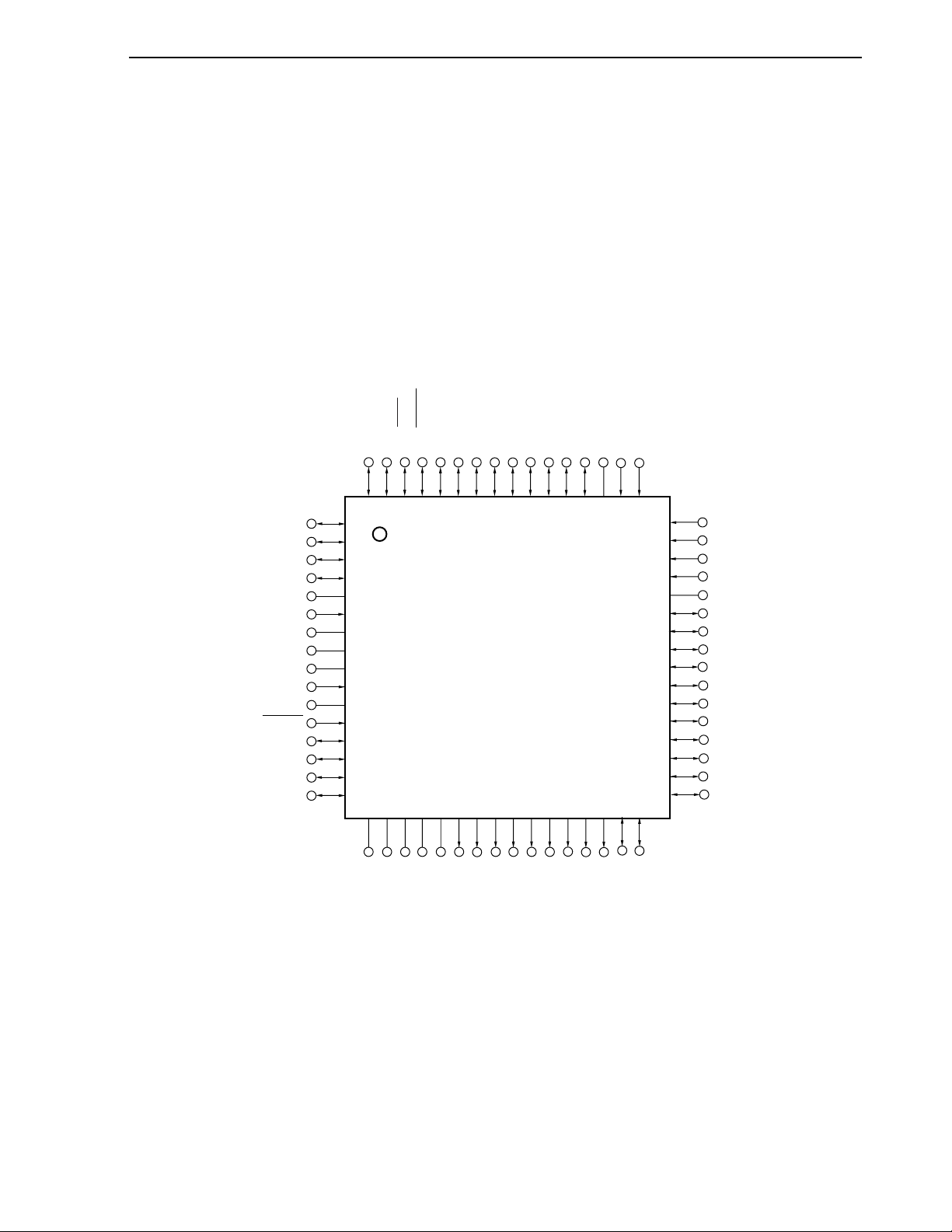
1.4 Pin Configuration (Top View)
CHAPTER 1 GENERAL
1.4.1 Pin configuration of
PD789426, 789436 Subseries (Top view)
µµµµ
64-pin plastic TQFP (fine pitch) (12 × 12)
PD789425GK-
µ
PD789426GK-
µ
PD789435GK-
µ
PD789436GK-
µ
PD78F9436GK-9ET
µ
×××
×××
×××
×××
P50
P51
P52
P53
PP
IC(V
XT1
XT2
V
V
X1
X2
RESET
P00/KR0
P01/KR1
P02/KR2
P03/KR3
-9ET
-9ET
-9ET
-9ET
)
DD
SS
P20
P21/BZO90
P22/SS20
P23/SCK20/ASCK20
P24/SO20/TxD20
P25/SI20/RxD20
P26/TO90
P30/INTP0/CPT90
P31/INTP1/TO50/TMI60
P32/INTP2/TO60
P33/INTP3/TO61
P10
P11
64 63 62 61 60 59 58 57 56 55 54 53 52 51 50
1
2
3
4
5
6
7
8
9
10
11
12
13
14
15
16
17 18 19 20 21 22 23 24 25 26 27 28 29 30 31
AVSSP60/ANI0
P61/ANI1
49
48
47
46
45
44
43
42
41
40
39
38
37
36
35
34
33
32
P62/ANI2
P63/ANI3
P64/ANI4
P65/ANI5
DD
AV
P72
P71
P70
P81
P80
P97
P96
P95
P94
P93
P92
CAPL
CAPH
LC0VLC1VLC2
V
COM0
COM1
S0S1S2S3S4
COM2
COM3
Cautions 1. Connect the IC (Internally Connected) pin directly to VSS.
2. Connect the AVDD pin to VDD.
3. Connect the AVSS pin to VSS.
Remark
The parenthesized values apply to the
User’s Manual U15075EJ1V0UM00
PD78F9436.
µ
P90
P91
27
Page 28

CHAPTER 1 GENERAL
1.4.2 Pin configuration of
PD789446, 789456 Subseries (Top view)
µµµµ
64-pin plastic TQFP (fine pitch) (12 × 12)
PD789445GK-
µ
PD789446GK-
µ
PD789455GK-
µ
PD789456GK-
µ
PD78F9456GK-9ET
µ
RESET
P00/KR0
P01/KR1
P02/KR2
P03/KR3
IC(V
×××
×××
×××
×××
P50
P51
P52
P53
PP
XT1
XT2
V
V
X1
X2
-9ET
-9ET
-9ET
-9ET
)
DD
SS
P20
P21/BZO90
P22/SS20
P23/SCK20/ASCK20
P24/SO20/TxD20
P25/SI20/RxD20
P26/TO90
P30/INTP0/CPT90
P31/INTP1/TO50/TMI60
P32/INTP2/TO60
P33/INTP3/TO61
P10
P11
64 63 62 61 60 59 58 57 56 55 54 53 52 51 50
1
2
3
4
5
6
7
8
9
10
11
12
13
14
15
16
17 18 19 20 21 22 23 24 25 26 27 28 29 30 31
AVSSP60/ANI0
P61/ANI1
49
48
47
46
45
44
43
42
41
40
39
38
37
36
35
34
33
32
P62/ANI2
P63/ANI3
P64/ANI4
P65/ANI5
DD
AV
P72
P71
P70
S14
S13
S12
S11
S10
S9
S8
S7
CAPL
CAPH
LC0VLC1VLC2
V
COM0
COM1
S0S1S2S3S4S5S6
COM2
COM3
Cautions 1. Connect the IC (Internally Connected) pin directly to VSS.
2. Connect the AVDD pin to VDD.
3. Connect the AVSS pin to VSS.
28
Remark
The parenthesized values apply to the
User’s Manual U15075EJ1V0UM00
PD78F9456.
µ
Page 29

CHAPTER 1 GENERAL
ANI0 to ANI5: Analog input P90 to P97
Note 1
:Port 9
ASCK20: Asynchronous serial input RESET: Reset
DD
AV
: Analog power supply RxD20: Receive data
SS
AV
: Analog ground SS20: Serial chip select
BZO90: Buzzer output S0 to S4, S5 to S14
Note 2
: Segment output
CAPH, CAPL: LCD power supply capacitance control SCK20: Serial clock
COM0 to COM3: Common output SI20: Serial input
CPT90: Capture trigger input SO20: Serial output
IC: Internally connected TMI60: Timer input
INTP0 to INTP3: External interrupt input TO90, TO50, TO60,
KR0 to KR3: Key return TO61: Timer output
P00 to P03: Port 0 TxD20: Transmit data
P10, P11: Port 1 V
P20 to P26: Port 2 V
P30 to P33: Port 3 V
P50 to P53: Port 5 V
DD
: Power supply
LC0
LC2
to V
PP
: Programming power supply
SS
: Ground
: LCD power supply
P60 to P65: Port 6 X1, X2: Crystal (main system clock)
P70 to P72: Port 7 XT1, XT2: Crystal (subsystem clock)
P80, P81
Note 1
:Port 8
Notes 1.
PD789426, 789436 Subseries only
µ
2.
PD789446, 789456 Subseries only
µ
User’s Manual U15075EJ1V0UM00
29
Page 30

CHAPTER 1 GENERAL
1.5 78K/0S Series Lineup
The products in the 78K/0S Series are listed below. The names enclosed in boxes are subseries names.
Products in mass production
Products under development
Y Subseries products support SMB.
Small-scale package, general-purpose applications
78K/0S
Series
44-pin
42-/44-pin
30-pin
28-pin
44-pin
44-pin
30-pin
30-pin
30-pin
30-pin
30-pin
30-pin
44-pin
52-pin
80-pin
80-pin
80-pin
64-pin
64-pin
64-pin
64-pin
64-pin
64-pin
µ
PD789046
µ
PD789026
µ
PD789074
µ
PD789014
Small-scale package, general-purpose applications and A/D converter
µ
µ
PD789177
µ
PD789167
µ
PD789156
PD789146
µ
PD789134A
µ
µ
PD789124A
PD789114A
µ
µ
PD789104A
Inverter control
PD789842
µ
VFD drive
µ
PD789871
LCD drive
µ
PD789488
µ
PD789417A
µ
PD789407A
µ
PD789456
µ
PD789446
µ
PD789436
µ
PD789426
µ
PD789316
µ
PD789306
PD789177Y
µ
PD789167Y
µ
PD789074 with added subsystem clock
µ
PD789014 with enhanced timer and increased ROM, RAM capacity
µ
PD789026 with enhanced timer
On-chip UART and capable of low voltage (1.8 V) operation
µ
PD789167 with enhanced A/D converter
µ
PD789104A with enhanced timer
µ
PD789146 with enhanced A/D converter
µ
PD789104A with added EEPROM
µ
PD789124A with enhanced A/D converter
RC oscillation version of the PD789104A
µ
PD789104A with enhanced A/D converter
µ
PD789026 with added A/D converter and multiplier
On-chip inverter controller and UART
Total display outputs: 25
A/D converter and on-chip voltage booster type LCD (28 × 4)
µ
PD789407A with enhanced A/D converter
A/D converter and resistance division type LCD (28 × 4)
µ
PD789446 with enhanced A/D converter
A/D converter and on-chip voltage booster type LCD (15 × 4)
PD789426 with enhanced A/D
µ
A/D converter and on-chip voltage booster type LCD (5 × 4)
RC oscillation version of the PD789306
On-chip voltage booster type LCD (24 × 4)
µ
µ
TM
30
144-pin
88-pin
80-pin
52-pin
52-pin
44-pin
44-pin
20-pin
20-pin
Dot LCD drive
PD789835
µ
µ
PD789830
ASSP
µ
PD789477
PD789467
µ
µ
PD789327
µ
PD78980364-pin
µ
PD789800
µ
PD789840
PD789861
µ
µ
PD789860
Segment/common outputs: 96
Segments: 40, commons: 16
µ
PD789488 with added remote control receiver and resistance division type LCD
For remote controller, with A/D converter and on-chip voltage booster type LCD
For remote controller, with SIO and resistance division type LCD
For PC keyboard, on-chip USB HUB function
For PC keyboard, on-chip USB function
For keypad, on-chip POC
RC oscillation version of the PD789860
For keyless entry, on-chip POC and key return circuit
User’s Manual U15075EJ1V0UM00
µ
Page 31

CHAPTER 1 GENERAL
The major functional differences among the subseries are listed below.
DD
Function
Subseries Name
µ
Small-scale
package,
generalpurpose
applications
Small-scale
package,
generalpurpose
applications
and A/D
converter
Inverter
control
VFD driveµPD789871 4 K t o 8 K 3 c h – 1 ch 1 ch – – 1 ch 33 2.7 V –
LCD drive
drive
ASSP
PD789046 16 K 1 ch
µ
PD789026 4 K t o 16 K
µ
PD789074 2 K t o 8 K
µ
PD789014 2 K t o 4 K 2 c h
µ
PD789177
µ
PD789167
µ
PD789156
µ
PD789146
µ
PD789134A
µ
PD789124A 4 c h
µ
PD789114A
µ
PD789104A
µ
PD789842 8 K t o 16 K 3 ch
µ
PD789488 32 K 8 ch 2 ch (UART:
µ
PD789417A
µ
PD789407A
µ
PD789456 – 6 ch
µ
PD789446 6 ch –
µ
PD789436 – 6 ch
µ
PD789426
µ
PD789316 RC-oscillation
µ
PD789306
µ
PD789835 24 K t o
µ
PD789830 24 K 1 ch 1 ch
µ
PD789477 24 K 3 ch 1 ch 8 ch 2 ch (UART:
µ
PD789467 1 ch – 18
µ
PD789327
µ
PD789800
µ
PD789840
µ
PD789861 RC-oscillation
µ
PD789860
ROM
Capacity
16 K to 24 K 3 ch 1 ch
8 K to 16 K
2 K to 8 K
12 K to
24 K
12 K to
16 K
8 K to 16 K
60 K
4 K to 24 K
8 K
4 K
8-Bit 16-B i t Watch WDT
1 ch 1 ch
−
−
1 ch
1 ch
Note
1 ch 1 ch 1 ch
3 ch
2 ch
6 ch – 3 ch 28 1.8 VDot LCD
2 ch –
−
1 ch 1 ch 8 ch
1 ch 1 ch
1 ch
−
8-Bit
10-Bit
A/D
A/D
1 ch
1 ch
−−
−
8 ch
8 ch
4 ch
4 ch
7 ch
6 ch
4 ch 1 c h 29 2.8 V
−
−
4 ch
−
−
4 ch
−
−
4 ch
−
−
−
7 ch
−
–
–
–1 ch (UART:
–
–
–
−
Serial
Interface
1 ch (UART:
1 ch)
1 ch (UART:
1 ch)
1 ch (UART:
1 ch)
1 ch)
1 ch (UART:
1 ch)
2 ch (UART:
1 ch)
1 ch)
1 ch)
1 ch 21
2 ch (USB:
1 ch)
– 14 1.8 V
V
I/O
MIN.
Value
34
1.8 V
24
22
31
20
30 4.0 V
45
43
30
40
23
30 2.7 V
45
31 4.0 V
On-chip
EEPROM
RC-oscillation
version
1.8 V
version
1.8 V On-chip LCD
version,
on-chip
EEPROM
On-chip
EEPROM
Remarks
−
−
−
−
−
–
−
−
10-bit timer: 1 channel
Note
User’s Manual U15075EJ1V0UM00 31
Page 32

1.6 Block Diagram
CHAPTER 1 GENERAL
1.6.1 Block diagram of
TO50/TMI60/
TMI60/TO50/
SCK20/ASCK20/P23
SO20/TxD20/P24
SI20/RxD20/P25
COM0 to COM3
P31
TO60/P32
TO61/P33
P31
TO90/P26
CPT90/P30
BZO90/P21
ANI0/P60 to
ANI5/P65
AV
DD
AV
SS
SS20/P22
S0 to S4
V
LC0
to V
LC2
CAPH
CAPL
PD789426, 789436 Subseries
µµµµ
8-bit
timer 50
8-bit
timer/event
counter 60
Cascaded
16-bit
timer/
event
counter
16-bit timer 90
Watch timer
Watchdog timer
A/D converter
Serial
Iinterface 20
LCD controller
driver
78K/0S
CPU core
RAM
ROM
(flash
memory)
RAM space
for LCD
data
Port 0
Port 1
Port 2
Port 3
Port 5
Port 6
Port 7
Port 8
Port 9
System control
Interrupt control
P00 to P03
P10, P11
P20 to P26
P30 to P33
P50 to P53
P60 to P65
P70 to P72
P80, P81
P90 to P97
RESET
X1
X2
XT1
XT2
INTP0/P30
INTP1/P31
INTP2/P32
INTP3/P33
KR0/P00 to
KR3/P03
Remarks 1.
32
VDDVSSIC
(V
The internal ROM capacity varies depending on the product.
2.
The parenthesized values apply to the
User’s Manual U15075EJ1V0UM00
PD78F9436.
µ
PP
)
Page 33

CHAPTER 1 GENERAL
1.6.2 Block diagram of
TO50/TMI60/
TMI60/TO50/
SCK20/ASCK20/P23
SO20/TxD20/P24
SI20/RxD20/P25
COM0 to COM3
P31
TO60/P32
TO61/P33
P31
TO90/P26
CPT90/P30
BZO90/P21
ANI0/P60 to
ANI5/P65
AV
DD
AV
SS
SS20/P22
S0 to S4
V
LC0
to V
LC2
CAPH
CAPL
PD789446, 789456 Subseries
µµµµ
8-bit
timer 50
8-bit
timer/event
counter 60
Cascaded
16-bit
timer/
event
counter
16-bit timer 90
Watch timer
Watchdog timer
A/D converter
Serial
Iinterface 20
LCD controller
driver
78K/0S
CPU core
RAM
ROM
(flash
memory)
RAM space
for LCD
data
Port 0
Port 1
Port 2
Port 3
Port 5
Port 6
Port 7
Port 8
Port 9
System control
Interrupt control
P00 to P03
P10, P11
P20 to P26
P30 to P33
P50 to P53
P60 to P65
P70 to P72
P80, P81
P90 to P97
RESET
X1
X2
XT1
XT2
INTP0/P30
INTP1/P31
INTP2/P32
INTP3/P33
KR0/P00 to
KR3/P03
Remarks 1.
VDDVSSIC
PP
)
(V
The internal ROM capacity varies depending on the product.
2.
The parenthesized values apply to the
User’s Manual U15075EJ1V0UM00
PD78F9456.
µ
33
Page 34

1.7 Overview of Functions
CHAPTER 1 GENERAL
Item
Internal memory
Minimum instructi on execution time • 0.4 µs/1.6 µs (@ 5.0 MHz operation with main system clock)
General-purpose registers 8 bits × 8 registers
Instruction set • 16-bi t operations
I/O ports Total: 40
Timers • 16-bit timer: 1 channel
A/D converter • 8-bi t resolution × 6 channels (µPD789426, 789446 Subseries)
Serial interfaces Switchable between 3-wire serial I/O mode and UART mode: 1 channel
LCD controller/driver • Segment signal outputs: 5 max.
Vectored interrupt
sources
Power supply voltage VDD = 1.8 to 5.5 V
Operating ambient temperature TA = −40 to +85°C
Package 64-pin plastic TQFP (f i ne pi tch) (12 × 12)
ROM
High-speed RAM 512 bytes
LCD display RAM 5 bytes 15 bytes
Maskable Internal: 9, external: 5
Non-maskable Internal: 1
µ
PD789425,
789435
Mask ROM Flash
12 KB 16 KB 12 KB 16 KB
• 122
• Bit manipulations (such as set, reset, and tes t )
• CMOS I/O: 30
• CM OS input: 6
• N-ch open-drain: 4
• 8-bit timer: 2 channels
• Watc h timer: 1 channel
• Watc hdog timer: 1 channel
• 10-bi t resolution × 6 channels (
• Common signal outputs: 4 max.
µ
PD789426,
789436
µ
s (@ 32.768 kHz operation with s ubsystem clock)
µ
PD78F9436µPD789445,
789455
Mask ROM Flash
memory
Total: 30
• CMOS I/O: 20
• CM OS input: 6
• N-ch open-drain: 4
µ
PD789436, 789456 Subseries)
• Segment signal outputs: 15 max.
• Common signal outputs: 4 max.
µ
PD789446,
789456
µ
PD78F9456
memory
34
User’s Manual U15075EJ1V0UM00
Page 35

An outline of the timer is shown below.
CHAPTER 1 GENERAL
Operation
mode
Function
Notes 1.
16-Bit
Timer
Interval timer – 1 channel 1 channel
External event
– – 1 channel – –
8–Bit
Timer 50
8-Bit
Timer 60
Watch Timer Watchdog
Timer
1 channel
Note 1
1 channel
counter
Timer outputs 1 1 2 – –
Square-wave
–12––
outputs
Capture 1 input – – – –
Interrupt
11111
sources
The watch timer can perform both watch timer and interval timer functions at the same time.
The watchdog timer has the watchdog timer and interval timer functions. However, use the watchdog
2.
timer by selecting either the watchdog timer function or interval timer function.
Note 2
User’s Manual U15075EJ1V0UM00 35
Page 36

[MEMO]
36 User’s Manual U15075EJ1V0UM00
Page 37

CHAPTER 2 PIN FUNCTIONS
2.1 List of Pin Functions
(1) Port pins (1/2)
Pin Name I/O Funct ion After R eset Alternat e Function
P00 to P03 I/O Port 0.
4-bit I/O port.
Input/output can be spec i f i ed i n 1-bi t units.
When used as an input port, an on-chip pull -up resistor can be
specified by means of pul l -up res i stor option register 0 (PU0) or
key return mode register 00 (KRM00).
P10 to P13 I/O Port 1.
4-bit I/O port.
Input/output can be spec i f i ed i n 1-bi t units.
When used as an input port, an on-chip pull -up resistor can be
specified by means of pul l -up res i stor option register 0 (PU0).
P20 –
P21 BZO90
P22 SS20
P23 SCK20/ASCK20
P24 SO20/TxD20
P25 SI20/RxD20
P26
P30 INTP0/CPT90
P31 INTP1/TO50/
P32 INTP2/TO60
P33
P50 to P53 I/O Port 5.
I/O Port 2.
7-bit I/O port.
Input/output can be spec i f i ed i n 1-bi t units.
When used as an input port, an on-chip pull -up resistor can be
specified by means of pul l -up res i stor option register B2 (PUB2).
I/O Port 3.
4-bit I/O port.
Input/output can be spec i f i ed i n 1-bi t units.
When used as an input port, an on-chip pull -up resistor can be
specified by means of pul l -up res i stor option register B3 (PUB3).
4-bit N-ch open-drain I/O port.
Input/output can be spec i f i ed i n 1-bi t units.
For a mask ROM version, an on-c hi p pul l -up resistor can be
specified by the mas k option.
Input KR0 to KR3
Input –
Input
TO90
Input
TMI60
INTP3/TO61
Input
−
P60 to P65 Input Port 6.
6-bit input port.
P70 to P72 I/O Port 7.
3-bit I/O port.
Input/output can be spec i f i ed i n 1-bi t units.
When used as an input port, an on-chip pull -up resistor can be
specified by means of pul l -up res i stor option register B7 (PUB7).
Input ANI0 to ANI5
Input
User’s Manual U15075EJ1V0UM00 37
−
Page 38

CHAPTER 2 PIN FUNCTIONS
(1) Port pins (2/2)
Pin Name I/O Funct ion After R eset Alternat e Function
Note
Note
I/O Port 8.
2-bit I/O port.
Input/output can be spec i f i ed i n 1-bi t units.
When used as an input port, an on-chip pull -up resistor can be
specified by means of pul l -up res i stor option register B8 (PUB8).
Note
I/O Port 9.
8-bit I/O port.
Input/output can be spec i f i ed i n 1-bi t units.
When used as an input port, an on-chip pull -up resistor can be
specified by means of pul l -up res i stor option register B9 (PUB9).
PD789426, 789436 Subseries only
µ
Input
Input
−
−
P80, P81
P90 to P97
38 User’s Manual U15075EJ1V0UM00
Page 39

CHAPTER 2 PIN FUNCTIONS
(2) Non-port pins
Pin Name I/O Funct ion After Reset Alternate Function
INTP0 P30/CPT90
INTP1 P31/TO50/TMI60
Input
External interrupt input for which the valid edge (ri sing edge,
falling edge, or both rising and falling edges) can be specified
Input
INTP2 P32/TO60
INTP3
P33/TO61
KR0 to KR3 Input Key return signal detection Input P00 to P03
SS20 Input Serial interface (SIO20) chip select Input P22
SCK20 I/O Serial interface 20 serial clock input/output Input P23/ASCK20
SI20 Input Serial interface 20 of SIO20 serial data input Input P25/RxD20
SO20 Output Serial interface 20 of SIO20 serial data output Input P24/TxD20
ASCK20 Input Serial clock input for asynchronous serial int erface Input P 23/SCK20
RxD20 Input Serial dat a i nput for asynchronous serial i nt erface Input P25/SI20
TxD20 Output Serial data output for asynchronous serial interface Input P24/SO20
TO90 Output 16-bit timer (TM90) output Input P26
CPT90 Input Capture edge input Input P30/INTP0
TO50 Out put 8-bit timer (TM50) output Input P 31/INTP1/TMI40
TO60 Out put Input P 32/INTP2
TO61 Output
8-bit timer (TM60) output
Input P 33/ INTP33
TMI60 Input External count clock input to timer 40 Input P 31/INTP1/TO50
ANI0 to ANI5 Input A/D converter analog input Input P60 to P65
S0 to S4 Output Output •−•
S5 to S14
Note
Output
COM0 to COM3 Output LCD controller/dri v er common signal output Output
LC0
to V
LC2
V
CAPH
CAPL
X1 Input
X2
XT1 Input
XT2
LCD controller/driver segment signal output
Output •−•
−
LCD driving voltage
− −
Capacitor connection pin for LCD dri ve
−
Connecting crystal res onator for main system clock oscillation
−
Connecting crystal res onator for subsystem clock oscillation
−
−
−
•−•
•−•
−
−
−
−
−
•−•
•−•
•−•
•−•
•−•
RESET I nput System reset input Input •−•
V
V
AV
AV
IC
V
DD
SS
DD
SS
PP
−
Positive power supply
−
Ground potential
−
A/D converter analog potenti al
−
A/D converter analog ground potenti al
−
Internally connected. Connect directly to VSS.
−
Sets flash memory programming mode. Applies high voltage
when a program is written or verifi ed. Connect directly to V
SS
in
−
−
•−•
•−•
−
−
−
−
•−•
•−•
•−•
normal operation mode.
Note
PD789446, 789456 Subseries only
µ
User’s Manual U15075EJ1V0UM00 39
Page 40

CHAPTER 2 PIN FUNCTIONS
2.2 Description of Pin Functions
2.2.1 P00 to P03 (Port 0)
These pins constitute a 4-bit I/O port. In addition, these pins enable key return signal detection.
Port 0 can be specified in the following operation modes in 1-bit units.
(1) Port mode
These pins constitute a 4-bit I/O port and can be set in the input or output port mode in 1-bit units by port
mode register 0 (PM0). When used as an input port, use of an on-chip pull-up resistor can be specified by
pull-up resistor option register 0 (PU0) in port units.
(2) Control mode
In this mode, P00 to P03 function as key return signal detection pins (KR0 to KR3).
2.2.2 P10, P11 (Port 1)
These pins constitute a 2-bit I/O port and can be set in the input or output port mode in 1-bit units by port mode
register 1 (PM1). When used as an input port, use of an on-chip pull-up resistor can be specified by pull-up resistor
option register 0 (PU0) in port units.
2.2.3 P20 to P26 (Port 2)
These pins constitute a 7-bit I/O port. In addition, these pins enable buzzer output, timer output, serial interface
data I/O, and serial clock I/O.
Port 2 can be specified in the following operation modes in 1-bit units.
(1) Port mode
In this mode, P20 to P26 function as a 7-bit I/O port. Port 2 can be set in the input or output port mode in 1bit units by port mode register 2 (PM2). When used as an input port, use of an on-chip pull-up resistor can
be specified by pull-up resistor option register B2 (PUB2) in 1-bit units.
(2) Control mode
In this mode, P20 to P26 function as the buzzer output, timer output, serial interface data I/O, and serial
clock I/O.
(a) Buzzer output
This is the buzzer output pin of 16-bit timer 90.
(b) TO90
This is the timer output pin of 16-bit timer 90.
(c) SI20, SO20
These are the serial data I/O pins of the serial interface.
(d) SCK20
This is the serial clock I/O pin of the serial interface.
(e) RxD20, TxD20
These are the serial data I/O pins of the asynchronous serial interface.
40 User’s Manual U15075EJ1V0UM00
Page 41

CHAPTER 2 PIN FUNCTIONS
(f) ASCK20
This is the serial clock input pin of the asynchronous serial interface.
Caution When using P20 to P26 as serial interface pins, the I/O mode and output latch must be set
according to the functions to be used. For the details of the setting, refer to Table 12-2 Settings
of Serial Interface 20 Operating Mode.
2.2.4 P30 to P33 (Port 3)
These pins constitute a 4-bit I/O port. In addition, they also function as timer I/O and external interrupt input.
Port 3 can be specified in the following operation mode in 1-bit units.
(1) Port mode
In this mode, P30 to P33 functions as a 4-bit I/O port. Port 3 can be set in the input or output port mode in
1-bit units by port mode register 3 (PM3). When used as an input port, use of an on-chip pull-up resistor can
be specified by pull-up resistor option register B3 (PUB3) in 1-bit units.
(2) Control mode
In this mode, P30 to P33 function as timer I/O and external interrupt input.
(a) TMI60
This is the external clock input pin to timer 60.
(b) TO50, TO60, TO61
These are the timer output pins of timer 50 and timer 60
(c) CPT90
This is the capture edge input pin of 16-bit timer 90.
(d) INTP0 to INTP3
These are external interrupt input pins for which valid edges (rising edge, falling edge, or both rising
and falling edges) can be specified.
2.2.5 P50 to P53 (Port 5)
These pins function as a 4-bit N-ch open-drain I/O port. Port 5 can be set in the input or output port mode in 1-bit
units by port mode register 5 (PM5). In the mask ROM version, use of an on-chip pull-up resistor can be specified by
a mask option.
2.2.6 P60 to P65 (Port 6)
This is a 6-bit input-only port. In addition to a general-purpose input port function, it has an A/D converter input
function.
(1) Port mode
In this mode, P60 to P65 function as 6-bit input-only port.
(2) Control mode
In this mode, P60 to P65 function as analog inputs (ANI0 to ANI5) of A/D converter.
User’s Manual U15075EJ1V0UM00
41
Page 42

CHAPTER 2 PIN FUNCTIONS
2.2.7 P70 to P72 (Port 7)
These pins constitute a 3-bit I/O port. Port 7 can be set in the input or output mode in 1-bit units by port mode
register 7 (PM7). When used as an input port, use of an on-chip pull-up resistor can be specified by pull-up resistor
option register B7 (PUB7) in port units.
2.2.8 P80, P81 (Port 8)
Note
These pins constitute a 2-bit I/O port. Port 8 can be set in the input or output mode in 1-bit units by port mode
register 8 (PM8). When used as an input port, use of an on-chip pull-up resistor can be specified by pull-up resistor
option register B8 (PUB8) in port units.
Only the µPD789426 and µPD789436 Subseries.
Note
2.2.9 P90 to P97 (Port 9)
Note
These pins constitute an 8-bit I/O port. Port 9 can be set in the input or output mode in 1-bit units by port mode
register 9 (PM9). When used as an input port, use of an on-chip pull-up resistor can be specified by pull-up resistor
option register B9 (PUB9) in port units.
Only the µPD789426 and µPD789436 Subseries.
Note
2.2.10 S0 to S14
Note
These pins are segment signal output pins for the LCD controller/driver.
S0 to S4 in the case of the µPD789426 and 789436 Subseries
Note
2.2.11 COM0 to COM3
These pins are common signal output pins for the LCD controller/driver.
2.2.12 V
LC0
to V
LC2
These pins are power supply voltage pins to drive the LCD.
2.2.13 CAPH, CAPL
These pins are capacitor connection pins to drive the LCD.
2.2.14 RESET
This pin inputs an active-low system reset signal.
2.2.15 X1, X2
These pins are used to connect a crystal resonator for main system clock oscillation.
To supply an external clock, input the clock to X1 and input the inverted signal to X2.
2.2.16 XT1, XT2
These pins are used to connect a crystal resonator for subsystem clock oscillation.
To supply an external clock, input the clock to XT1 and input the inverted signal to XT2.
42 User’s Manual U15075EJ1V0UM00
Page 43

CHAPTER 2 PIN FUNCTIONS
2.2.17 V
DD
This is the positive power supply pin.
2.2.18 V
SS
This is the ground pin.
µµµµ
2.2.19 V
PP
(
PD78F9436, 78F9456 only)
A high voltage should be applied to this pin when the flash memory programming mode is set and when the
program is written or verified.
Directly connect this pin to V
SS
in the normal operation mode.
2.2.20 IC (mask ROM version only)
The IC (Internally Connected) pin is used to set the
PD789426, 789436, 789446, and 789456 Subseries in the
µ
test mode before shipment. In the normal operation mode, directly connect this pin to the VSS pin with as short a
wiring length as possible.
If a potential difference is generated between the IC pin and VSS pin due to a long wiring length, or an external
noise superimposed on the IC pin, the user program may not run correctly.
Directly connect the IC pin to the VSS pin.
•
IC
V
SS
Keep short
User’s Manual U15075EJ1V0UM00 43
Page 44

CHAPTER 2 PIN FUNCTIONS
2.3 Pin Input/Output Circuits and Recommended Connection of Unused Pins
The input/output circuit type of each pin and recommended connection of unused pins are shown in Table 2-1.
For the input/output circuit configuration of each type, see Figure 2-1.
Table 2-1. Types of Pin Input/Output Circuits
Pin Name I/O Circuit
I/O Recommended Connection of Unused Pins
Type
P00/KR0 to P03/KR3 8-A
P10, P11 5-A
P20
8-A
I/O
Input: Independently connect to V
Output: Leave open.
P21/BZO90
P22/SS20
P23/SCK20/ASCK20
P24/SO20/TxD20
P25/SI20/RxD20
P26/TO90
P30/INPT0/CPT90
P31/INPT1/TO50/TMI60
Input: Independently connect to V
Output: Leave open.
P32/INPT2/TO60
P33/INPT3/TO61
P50 to P53
(Mask ROM version)
P50 to P53
13-W
13-V
Input: Independently connect to V
Output: Leave open.
(Flash memory version)
P60/ANI0 to P65/ANI5 9-C Input Connect directly t o VDD or VSS.
P70 to P72
P80, P81
P90 to P97
S0 to S4
S0 to S14
Note 1
Note 1
Note 1
Note 2
COM0 to COM3 18
LC0
to V
LC2
V
5-A I/O Input: Independently connect to VDD or VSS via a resistor.
Output: Leave open.
17 Output
Leave open.
•−•
−
CAPH, CAPL
XT1 Input Connect to VSS.
XT2 Leave open.
SS
AV
DD
AV
−
Connect to VSS.
Connect to V
DD
.
RESET 2 Input
IC
V
−
PP
•−• Connect directl y to V
SS
.
DD
or VSS via a resistor.
SS
via a resistor.
DD
via a resistor.
−
Notes 1.
When using the
When using the µPD789446 and 789456 Subseries
2.
PD789426 and 789436 Subseries
µ
44 User’s Manual U15075EJ1V0UM00
Page 45

CHAPTER 2 PIN FUNCTIONS
Figure 2-1. Pin Input/Output Circuits
Type 2 Type 13-V
Output data
Output disable
IN/OUT
N-ch
IN
Schmitt-triggered input with hysteresis characteristics
Input enable
Type 5-A Type 13-W
V
DD
Pull-up
enable
Data
P-ch
DD
V
P-ch
Output data
Output disable
IN/OUT
Output
disable
N-ch
V
SS
Input enable
Input
enable
Type 8-A Type 17
DD
V
V
LC0
Pull-up
enable
V
Data
DD
P-ch
P-ch
V
LC1
SEG
data
IN/OUT
Output
disable
N-ch
V
SS
V
LC2
Middle-voltage
P-ch
P-ch
N-ch
N-ch
V
Middle-voltage
input buffer
Pull-up resistor
(mask option)
V
input buffer
P-ch
N-ch
SS
N-ch
SS
DD
V
IN/OUT
P-ch
OUT
N-ch
Type 9-C Type 18
V
V
REF
Comparator
+
-
Input
VLC1
COM
data
VLC2
IN
P-ch
N-ch
AV
SS
(Threshold voltage)
enable
User’s Manual U15075EJ1V0UM00 45
LC0
P-ch
N-ch
N-ch
P-ch
P-ch
N-ch
P-ch
N-ch
N-ch
OUT
P-ch
Page 46

[MEMO]
46 User’s Manual U15075EJ1V0UM00
Page 47

CHAPTER 3 CPU ARCHITECTURE
3.1 Memory Space
The µPD789426, 789436, 789446, and 789456 Subseries can access 64 KB of memory space. Figures 3-1
through 3-6 show the memory maps.
Data
memory space
FFFFH
FF00H
FEFFH
FD00H
FCFFH
FA05H
FA04H
FA00H
F9FFH
3000H
2FFFH
Figure 3-1. Memory Map (
Special function registers
256 × 8 bits
Internal high-speed RAM
512 × 8 bits
Reserved
LCD display RAM
5 × 4 bits
Reserved
µµµµ
PD789425, 789435)
2FFFH
Program area
Program
memory space
0000H
Internal ROM
12288 × 8 bits
User’s Manual U15075EJ1V0UM00 47
0080H
007FH
0040H
003FH
0022H
0021H
0000H
CALLT table area
Program area
Vector table area
Page 48

CHAPTER 3 CPU ARCHITECTURE
Data
memory space
FFFFH
FF00H
FEFFH
FD00H
FCFFH
FA05H
FA04H
FA00H
F9FFH
4000H
3FFFH
Figure 3-2. Memory Map (
Special function registers
256 × 8 bits
Internal high-speed RAM
512 × 8 bits
Reserved
LCD display RAM
5 × 4 bits
Reserved
µµµµ
PD789426, 789436)
3FFFH
Program area
Program
memory space
0000H
Internal ROM
16384 × 8 bits
0080H
007FH
0040H
003FH
0022H
0021H
0000H
CALLT table area
Program area
Vector table area
48 User’s Manual U15075EJ1V0UM00
Page 49

CHAPTER 3 CPU ARCHITECTURE
Data
memory space
FFFFH
FF00H
FEFFH
FD00H
FCFFH
FA05H
FA04H
FA00H
F9FFH
4000H
3FFFH
Figure 3-3. Memory Map (
Special function registers
256 × 8 bits
Internal high-speed RAM
512 × 8 bits
Reserved
LCD display RAM
5 × 4 bits
Reserved
µµµµ
PD78F9436)
3FFFH
Program area
Program
memory space
0000H
Flash memory
16384 × 8 bits
0080H
007FH
0040H
003FH
0022H
0021H
0000H
CALLT table area
Program area
Vector table area
User’s Manual U15075EJ1V0UM00 49
Page 50

CHAPTER 3 CPU ARCHITECTURE
Data
memory space
FFFFH
FF00H
FEFFH
FD00H
FCFFH
FA0FH
FA0EH
FA00H
F9FFH
3000H
2FFFH
Figure 3-4. Memory Map (
Special function registers
256 × 8 bits
Internal high-speed RAM
512 × 8 bits
Reserved
LCD display RAM
15 × 4 bits
Reserved
µµµµ
PD789445, 789455)
2FFFH
Program area
Program
memory space
0000H
Internal ROM
12288 × 8 bits
0080H
007FH
0040H
003FH
0022H
0021H
0000H
CALLT table area
Program area
Vector table area
50 User’s Manual U15075EJ1V0UM00
Page 51

CHAPTER 3 CPU ARCHITECTURE
Data
memory space
FFFFH
FF00H
FEFFH
FD00H
FCFFH
FA0FH
FA0EH
FA00H
F9FFH
4000H
3FFFH
Figure 3-5. Memory Map (
Special function registers
256 × 8 bits
Internal high-speed RAM
512 × 8 bits
Reserved
LCD display RAM
15 × 4 bits
Reserved
µµµµ
PD789446, 789456)
3FFFH
Program area
Program
memory space
0000H
Internal ROM
16384 × 8 bits
0080H
007FH
0040H
003FH
0022H
0021H
0000H
CALLT table area
Program area
Vector table area
User’s Manual U15075EJ1V0UM00 51
Page 52

CHAPTER 3 CPU ARCHITECTURE
Data
memory space
FFFFH
FF00H
FEFFH
FD00H
FCFFH
FA0FH
FA0EH
FA00H
F9FFH
4000H
3FFFH
Figure 3-6. Memory Map (
Special function registers
256 × 8 bits
Internal high-speed RAM
512 × 8 bits
Reserved
LCD display RAM
15 × 4 bits
Reserved
µµµµ
PD78F9456)
3FFFH
Program area
Program
memory space
0000H
Flash memory
16384 × 8 bits
0080H
007FH
0040H
003FH
0022H
0021H
0000H
CALLT table area
Program area
Vector table area
52 User’s Manual U15075EJ1V0UM00
Page 53

CHAPTER 3 CPU ARCHITECTURE
3.1.1 Internal program memory space
The internal program memory space stores programs and table data. This space is usually addressed by the
program counter (PC).
The
PD789426, 789436, 789446, and 789456 Subseries provide internal ROM (or flash memory) with the
µ
following capacity for each product.
Table 3-1. Internal ROM Capacity
Part Number Internal ROM
Structure Capacity
µ
PD789425, 789435,
789445, 789455
µ
PD789426, 789436,
789446, 789456
µ
PD78F9436, 78F9456 Flash memory 16384 × 8 bits
Mask ROM
12288 × 8 bits
16384 × 8 bits
The following areas are allocated to the internal program memory space.
(1) Vector table area
The 34-byte area of addresses 0000H to 0021H is reserved as a vector table area. This area stores
program start addresses to be used when branching by the RESET input or an interrupt request generation.
Of a 16-bit program address, the lower 8 bits are stored in an even address, and the higher 8 bits are stored
in an odd address.
Table 3-2. Vector Table
Vector Table Address Interrupt Request Vector Table Address Interrupt Request
0000H RESET input 0014H INTWTI
0004H INTWDT 0016H INTTM90
0006H INTP 0 0018H INTTM50
0008H INTP 1 001AH INTTM60
000AH INTP2 001CH INTAD0
000CH INTP3 001EH INTWT
000EH INTSR20/INTCSI20 0020H INTKR00
0012H INTST20
(2) CALLT instruction table area
The subroutine entry address of a 1-byte call instruction (CALLT) can be stored in the 64-byte area of
addresses 0040H to 007FH.
User’s Manual U15075EJ1V0UM00 53
Page 54

CHAPTER 3 CPU ARCHITECTURE
3.1.2 Internal data memory (internal high-speed RAM) space
The
PD789426, 789436, 789446, and 789456 Subseries products incorporate the following RAM.
µ
(1) Internal high-speed RAM
Internal high-speed RAM is incorporated in the area between FD00H and FEFFH.
The internal high-speed RAM is also used as a stack.
(2) LCD display RAM
LCD display RAM is incorporated.
The LCD display RAM can also be used as ordinary RAM.
Each subseries incorporates LCD display RAM with the following capacity.
Table 3-3. LCD Display RAM Capacity
Subseries Name Area Capacity
µ
PD789426, 789436 Subseries FA00H to FA04H 5 × 4 bits
µ
PD789446, 789456 Subseries FA00H to FA0EH 15 × 4 bits
3.1.3 Special function register (SFR) area
Special function registers (SFRs) of on-chip peripheral hardware are allocated in the area between FF00H to
FFFFH (see
Table 3-4
).
54 User’s Manual U15075EJ1V0UM00
Page 55

CHAPTER 3 CPU ARCHITECTURE
3.1.4 Data memory addressing
The
PD789426, 789436, 789446, and 789456 Subseries are provided with a variety of addressing modes to
µ
make memory manipulation as efficient as possible. At the addresses corresponding to data memory area (FD00H
to FFFFH) especially, specific addressing modes that correspond to the particular function an area, such as the
special function registers are available. Figures 3-7 through 3-12 show the data memory addressing modes.
FFFFH
FF20H
FF1FH
FF00H
FEFFH
FE20H
FE1FH
FD00H
FCFFH
FA05H
FA04H
Figure 3-7. Data Memory Addressing (
Special function registers (SFRs)
256 × 8 bits
Internal high-speed RAM
512 × 8 bits
Reserved
LCD display RAM
5 × 4 bits
SFR addressing
µµµµ
PD789425, 789435)
Short direct
addressing
Direct adressing
Register indirect
addressing
Based addressing
FA00H
F9FFH
3000H
2FFFH
0000H
Reserved
Internal ROM
12288 × 8 bits
User’s Manual U15075EJ1V0UM00 55
Page 56

CHAPTER 3 CPU ARCHITECTURE
FFFFH
FF20H
FF1FH
FF00H
FEFFH
FE20H
FE1FH
FD00H
FCFFH
FA05H
FA04H
Figure 3-8. Data Memory Addressing (
Special function registers (SFRs)
256 × 8 bits
Internal high-speed RAM
512 × 8 bits
Reserved
LCD display RAM
5 × 4 bits
SFR addressing
µµµµ
PD789426, 789436)
Short direct
addressing
Direct addressing
Register indirect
addressing
Based addressing
FA00H
F9FFH
4000H
3FFFH
0000H
Reserved
Internal ROM
16384 × 8 bits
56 User’s Manual U15075EJ1V0UM00
Page 57

CHAPTER 3 CPU ARCHITECTURE
FFFFH
FF20H
FF1FH
FF00H
FEFFH
FE20H
FE1FH
FD00H
FCFFH
FA05H
FA04H
Figure 3-9. Data Memory Addressing (
Special function registers (SFRs)
256 × 8 bits
Internal high-speed RAM
512 × 8 bits
Reserved
LCD display RAM
5 × 4 bits
SFR addressing
µµµµ
PD78F9436)
Short direct
addressing
Direct addressing
Register indirect
addressing
Based addressing
FA00H
F9FFH
4000H
3FFFH
0000H
Reserved
Flash memory
16384 × 8 bits
User’s Manual U15075EJ1V0UM00 57
Page 58

CHAPTER 3 CPU ARCHITECTURE
FFFFH
FF20H
FF1FH
FF00H
FEFFH
FE20H
FE1FH
FD00H
FCFFH
FA0FH
FA0EH
Figure 3-10. Data Memory Addressing (
Special function registers (SFRs)
256 × 8 bits
Internal high-speed RAM
512 × 8 bits
Reserved
LCD display RAM
15 × 4 bits
SFR addressing
µµµµ
PD789445, 789455)
Short direct
addressing
Direct addressing
Register indirect
addressing
Based addressing
FA00H
F9FFH
3000H
2FFFH
0000H
Reserved
Internal ROM
12288 × 8 bits
58 User’s Manual U15075EJ1V0UM00
Page 59

CHAPTER 3 CPU ARCHITECTURE
FFFFH
FF20H
FF1FH
FF00H
FEFFH
FE20H
FE1FH
FD00H
FCFFH
FA0FH
FA0EH
Figure 3-11. Data Memory Addressing (
Special function registers (SFRs)
256 × 8 bits
Internal high-speed RAM
512 × 8 bits
Reserved
LCD display RAM
15 × 4 bits
SFR addressing
µµµµ
PD789446, 789456)
Short direct
addressing
Direct addressing
Register indirect
addressing
Based addressing
FA00H
F9FFH
4000H
3FFFH
0000H
Reserved
Internal ROM
16384 × 8 bits
User’s Manual U15075EJ1V0UM00 59
Page 60

CHAPTER 3 CPU ARCHITECTURE
FFFFH
FF20H
FF1FH
FF00H
FEFFH
FE20H
FE1FH
FD00H
FCFFH
FA0FH
FA0EH
Figure 3-12. Data Memory Addressing (
Special function registers (SFRs)
256 × 8 bits
Internal high-speed RAM
512 × 8 bits
Reserved
LCD display RAM
15 × 4 bits
SFR addressing
µµµµ
PD78F9456)
Short direct
addressing
Direct addressing
Register indirect
addressing
Based addressing
FA00H
F9FFH
4000H
3FFFH
0000H
Reserved
Flash memory
16384 × 8 bits
60 User’s Manual U15075EJ1V0UM00
Page 61

CHAPTER 3 CPU ARCHITECTURE
3.2 Processor Registers
The µPD789426, 789436, 789446, and 789456 Subseries provide the following on-chip processor registers.
3.2.1 Control registers
The control registers contain special functions to control the program sequence statuses and stack memory. The
program counter, program status word, and stack pointer are control registers.
(1) Program counter (PC)
The program counter is a 16-bit register that holds the address information of the next program to be
executed.
In normal operation, the PC is automatically incremented according to the number of bytes of the instruction
to be fetched. When a branch instruction is executed, immediate data or register contents are set.
RESET input sets the reset vector table values at addresses 0000H and 0001H to the program counter.
Figure 3-13. Program Counter Configuration
015
PC14PC15PC PC13 PC12 PC11 PC10 PC9 PC8 PC7 PC6 PC5 PC4 PC3 PC2 PC1 PC0
(2) Program status word (PSW)
The program status word is an 8-bit register consisting of various flags to be set/reset by instruction
execution.
The program status word contents are automatically stacked upon interrupt request generation or PUSH
PSW instruction execution and are automatically restored upon execution of the RETI and POP PSW
instructions.
RESET input sets PSW to 02H.
Figure 3-14. Program Status Word Configuration
70
IE
PSW
Z 0 AC 0 0 1 CY
User’s Manual U15075EJ1V0UM00 61
Page 62

CHAPTER 3 CPU ARCHITECTURE
(a) Interrupt enable flag (IE)
This flag controls interrupt request acknowledgement operations of the CPU.
When 0, IE is set to the interrupt disable status (DI), and interrupt requests other than non-maskable
interrupt are all disabled.
When 1, IE is set to the interrupt enable status (EI). Interrupt request acknowledgement enable is
controlled with an interrupt mask flag for various interrupt sources.
IE is reset (0) upon DI instruction execution or interrupt acknowledgment and is set (1) upon EI
instruction execution.
(b) Zero flag (Z)
When the operation result is zero, this flag is set (1). It is reset (0) in all other cases.
(c) Auxiliary carry flag (AC)
If the operation result has a carry from bit 3 or a borrow at bit 3, this flag is set (1). It is reset (0) in all
other cases.
(d) Carry flag (CY)
This flag stores overflow and underflow upon add/subtract instruction execution. It stores the shift-out
value upon rotate instruction execution and functions as a bit accumulator during bit manipulation
instruction execution.
62 User’s Manual U15075EJ1V0UM00
Page 63

CHAPTER 3 CPU ARCHITECTURE
(3) Stack pointer (SP)
This is a 16-bit register to hold the start address of the memory stack area. Only the internal high-speed
RAM area can be set as the stack area.
Figure 3-15. Stack Pointer Configuration
SP14SP15SP SP13 SP12 SP11 SP10 SP9 SP8 SP7 SP6 SP5 SP4 SP3 SP2 SP1 SP0
The SP is decremented ahead of write (save) to the stack memory and is incremented after read (restore)
from the stack memory.
Each stack operation saves/restores data as shown in Figures 3-16 and 3-17.
Caution Since RESET input makes the SP contents undefined, be sure to initialize the SP before
instruction execution.
Figure 3-16. Data to Be Saved to Stack Memory
015
SP SP _ 2
SP _ 2
SP _ 1
SP
SP
SP + 1
PUSH rp
instruction
Lower
register pairs
Higher
register pairs
SP SP _ 2
SP _ 2
SP _ 1
SP
CALL, CALLT
instructions
PC7 to PC0
PC15 to PC8
Figure 3-17. Data to Be Restored from Stack Memory
instruction
Lower
register pairs
Higher
register pairs
SP
SP + 1
RET instructionPOP rp
PC7 to PC0
PC15 to PC8
SP SP _ 3
SP _ 3
SP _ 2
SP _ 1
SP
SP
SP + 1
Interrupt
PC7 to PC0
PC15 to PC8
PSW
RETI instruction
PC7 to PC0
PC15 to PC8
SP SP + 2
SP SP + 2
User’s Manual U15075EJ1V0UM00 63
SP + 2
SP SP + 3
PSW
Page 64

CHAPTER 3 CPU ARCHITECTURE
3.2.2 General-purpose registers
The general-purpose registers consist of eight 8-bit registers (X, A, C, B, E, D, L, and H).
Each register can be used as an 8-bit register, or two 8-bit registers in pairs can be used as a 16-bit register (AX,
BC, DE, and HL).
General-purpose registers can be described in terms of function names (X, A, C, B, E, D, L, H, AX, BC, DE, or
HL) or absolute names (R0 to R7 and RP0 to RP3).
Figure 3-18. General-Purpose Register Configuration
(a) Absolute names
16-bit processing 8-bit processing
R7
RP3
R6
R5
RP2
R4
R3
RP1
R2
R1
RP0
R0
15 0 7 0
(b) Function names
16-bit processing 8-bit processing
H
HL
L
D
DE
BC
E
B
C
AX
15 0 7 0
64 User’s Manual U15075EJ1V0UM00
A
X
Page 65

CHAPTER 3 CPU ARCHITECTURE
3.2.3 Special function registers (SFRs)
Unlike a general-purpose register, each special function register has a special function.
The special function registers are allocated in the 256-byte area of FF00H to FFFFH.
Special function registers can be manipulated, like general-purpose registers, by operation, transfer, and bit
manipulation instructions. The manipulatable bit units (1, 8, and 16) differ depending on the special function register
type.
The manipulatable bits can be specified as follows.
• 1-bit manipulation
Describes a symbol reserved by the assembler for the 1-bit manipulation instruction operand (sfr.bit). This
manipulation can also be specified with an address.
• 8-bit manipulation
Describes a symbol reserved by the assembler for the 8-bit manipulation instruction operand (sfr). This
manipulation can also be specified with an address.
• 16-bit manipulation
Describes a symbol reserved by the assembler for the 16-bit manipulation instruction operand. When
addressing an address, describe an even address.
Table 3-4 lists the special function registers. The meanings of the symbols in this table are as follows:
• Symbol
Indicates the addresses of the implemented special function registers. The symbols shown in this column are
the reserved words of the assembler, and have already been defined in the header file called “sfrbit.h” of the C
compiler. Therefore, these symbols can be used as instruction operands if an assembler or integrated
debugger is used.
•R/W
Indicates whether the special function register in question can be read or written.
R/W: Read/write
R: Read only
W: Write only
• Bit manipulation unit
Indicates the bit units (1, 8, 16) in which the special function register in question can be manipulated.
• After reset
Indicates the status of the special function register when the RESET signal is input.
User’s Manual U15075EJ1V0UM00 65
Page 66

CHAPTER 3 CPU ARCHITECTURE
Table 3-4. Special Function Register List (1/2)
FF00H Port 0 P0
R/W
FF01H Port 1 P1
FF02H Port 2 P2
FF03H Port 3 P3
FF05H Port 5 P5
FF06H Port 6 P6 R
FF07H Port 7 P7
Note 1
FF08H
FF09H
Port 8
Port 9
Note 1
P8
P9
FF0CH 8-bit compare register 60 CR60
CR6
Note 2
R/W
FF0DH 8-bit compare register 50 CR50
FF0EH 8-bit timer counter 60 TM60
TM6
Note 2
FF0FH 8-bit timer counter 50 TM50
Transmit shift regis ter 20 TXS20 W
SIO20
Receive buffer register 20 RXB20
Note 5
FF14H
A/D conversion result regi ster 0
ADCR0
FF15H
Note 2
FF16H
16-bit compare register 90
CR90
FF17H
Note 2
FF18H
16-bit timer counter 90
TM90
FF19H
Note 2
FF1AH 16-bit capture register 90
TCP90
FF1BH
FF20H Port mode register 0 PM0
R/W
FF21H Port mode register 1 PM1
FF22H Port mode register 2 PM2
FF23H Port mode register 3 PM3
FF25H Port mode register 5 PM5
Bit Manipulation UnitAddress Special Function Register (SFR) Name Symbol R/W
After Reset
1 Bit 8 Bits 16 Bits
√√−
00H
√√−
√√−
√√−
√√−
√√−
√√−
√√−
√√−
Notes 3, 4
W
−√
√
Undefined
−√
Notes 3, 4
R
−√
√
00H
−√
−√−
R
R
W
R
−√−
Notes 3
−√
−−
−−
−−
√
Notes 3, 4
√
Notes 3, 4
√
√
Note 3
√√−
FFHFF10H
Undefined
0000H
FFFFH
0000H
Undefined
FFH
√√−
√√−
√√−
√√−
PD789426 and 789436 Subseries only.
Notes 1.
µ
Name of SFR dedicated for 16-bit access.
2.
Only in short direct addressing, 16-bit access is possible.
3.
These are 16-bit access dedicated registers, however, 8-bit access is possible. When performing 8-bit
4.
access, access using direct addressing.
When used as an 8-bit A/D converter (µPD789426 and 789446 Subseries), only 8-bit access is
5.
possible. In this case, the address is FF15H.
When used as a 10-bit A/D converter (µPD789436 and 789456 Subseries), only 16-bit access is
possible. When the µPD78F9436, a flash memory version of the µPD789425 or µPD789426, is used,
this register can be accessed in 8-bit units. However, only an object file assembled with the
PD789425 or µPD789426 can be used. The same is also true for the µPD78F9456, a flash memory
µ
version of the µPD789445 or µPD789446: this register can be accessed in 8-bit units, but only an
object file assembled with the µPD789445 or µPD789446 can be used.
66 User’s Manual U15075EJ1V0UM00
Page 67

CHAPTER 3 CPU ARCHITECTURE
Table 3-4. Special Function Register List (2/2)
FF27H Port mode register 7 PM7
FF28H
FF29H
Port mode register 8
Port mode register 9
Note
Note
PM8
PM9
R/W
FF32H Pull-up resistor option regi ster B2 PUB2
FF33H Pull-up resistor option regi ster B3 PUB3
FF37H Pull-up resistor option regi ster B7 PUB7
FF38H
FF39H
Pull-up resistor option register B8
Pull-up resistor option register B9
Note
Note
PUB8
PUB9
FF42H Watchdog timer clock select register WDCS
FF48H 16-bit timer mode control regi ster 90 TMC90
FF49H Buzzer output control regi ster 90 BZC90
FF4AH Watch timer mode cont rol regi ster WTM
FF4CH 8-bit compare register H60 CRH60 W
FF4DH 8-bit ti m er mode control register 50 TMC50
R/W
FF4EH 8-bit timer mode cont rol regi s ter 60 TMC60
FF4FH Carrier generat or out put control register 60 TCA60 W
FF70H Asynchronous serial interface mode register 20 ASIM20 R/W
FF71H Asynchronous serial interface status register 20 ASIS20 R
FF72H Serial operation mode register 20 CSIM20
R/W
FF73H Baud rate generator control register 20 BRGC20
FF80H A/D converter mode regis t er 0 ADM0
FF84H Analog input channel speci f i cation register 0 ADS0
FFB0H LCD display mode regist er 0 LCDM0
FFB2H LCD clock c ontrol register 0 LCDC0
FFB3H LCD voltage amplification control register 0 LCDVA0
FFE0H Interrupt request flag regis ter 0 IF0
FFE1H Interrupt request flag regis ter 1 IF1
FFE4H Interrupt mask flag regi s ter 0 MK0
FFE5H Interrupt mask flag regi s ter 1 MK1
FFECH External int errupt mode register 0 INTM0
FFEDH External int errupt mode register 1 INTM1
FFF0H Suboscillation mode register SCKM
FFF2H Subcloc k control register CSS
FFF5H Key ret urn mode register 00 KRM00
FFF7H Pull-up resist or option regist er 0 PU0
FFF9H Watc hdog t i mer mode register WDTM
FFFAH Oscillation stabilization time select register OSTS
FFFBH Processor clock control register PCC
Bit Manipulation UnitAddress S pec i al Function Register (SFR) Name Symbol R/W
1 Bit 8 Bits 16 Bits
√√−
√√−
√√−
√√−
√√−
√√−
√√−
√√−
−√−
√√−
√√−
√√−
−√−
√√−
√√−
√√−
√√−
√√−
√√−
−√−
√√−
√√−
√√−
√√−
√√−
√√−
√√−
√√−
√√−
−√−
−√−
√√−
√√−
√√−
√√−
√√−
−√−
√√−
After Reset
FFH
00H
Undefined
00H
FFH
00H
04H
02H
Note
PD789426 and 789436 Subseries only.
µ
User’s Manual U15075EJ1V0UM00 67
Page 68

CHAPTER 3 CPU ARCHITECTURE
3.3 Instruction Address Addressing
An instruction address is determined by the program counter (PC) contents. The PC contents are normally
incremented (+1 for each byte) automatically according to the number of bytes of an instruction to be fetched each
time another instruction is executed. When a branch instruction is executed, the branch destination information is set
to the PC and branched by the following addressing (for details of each instruction, refer to
Instructions User’s Manual (U11047E)
).
3.3.1 Relative addressing
[Function]
The value obtained by adding 8-bit immediate data (displacement value: jdisp8) of an instruction code to the
start address of the following instruction is transferred to the program counter (PC) and branched. The
displacement value is treated as signed two’s complement data (–128 to +127) and bit 7 becomes a sign bit.
This means that information is relatively branched to a location between –128 and +127, from the start
address of the next instruction when relative addressing is used.
This function is carried out when the BR $addr16 instruction or a conditional branch instruction is executed.
[Illustration]
78K/0S Series
15 0
PC
+
15 0
α
15 0
PC
When S = 0, α indicates all bits 0.
When S = 1, α indicates all bits 1.
876
S
jdisp8
...
PC is the start address of
the next instruction of
a BR instruction.
68 User’s Manual U15075EJ1V0UM00
Page 69

CHAPTER 3 CPU ARCHITECTURE
3.3.2 Immediate addressing
[Function]
Immediate data in the instruction word is transferred to the program counter (PC) and branched.
This function is carried out when the CALL !addr16 or BR !addr16 instruction is executed.
CALL !addr16 and BR !addr16 instructions can be branched to any location in the memory space.
[Illustration]
In case of CALL !addr16 and BR !addr16 instructions
70
CALL or BR
Low Addr.
High Addr.
15 0
PC
87
User’s Manual U15075EJ1V0UM00 69
Page 70

CHAPTER 3 CPU ARCHITECTURE
3.3.3 Table indirect addressing
[Function]
Table contents (branch destination address) of the particular location to be addressed by the lower 5-bit
immediate data of an instruction code from bit 1 to bit 5 are transferred to the program counter (PC) and
branched.
This function is carried out when the CALLT [addr5] instruction is executed. The instruction enables a branch
to any location in the memory space by referring to the addresses stored in the memory table at 40H to 7FH.
[Illustration]
765 10
Instruction code
ta
4–0
001
Effective address
Effective address + 1
15 1
0100000000
Memory (Table)
70
Low Addr.
High Addr.
15 0
PC
87
87
65 0
0
3.3.4 Register addressing
[Function]
The register pair (AX) contents to be specified with an instruction word are transferred to the program counter
(PC) and branched.
This function is carried out when the BR AX instruction is executed.
[Illustration]
70
rp
15 0
PC
AX
07
87
70 User’s Manual U15075EJ1V0UM00
Page 71

CHAPTER 3 CPU ARCHITECTURE
3.4 Operand Address Addressing
The following various methods are available to specify the register and memory (addressing) which undergo
manipulation during instruction execution.
3.4.1 Direct addressing
[Function]
The memory indicated with immediate data in an instruction word is directly addressed.
[Operand format]
Identifier Description
addr16 Label or 16-bit immediate data
[Description example]
MOV A, !FE00H; When setting !addr16 to FE00H
[Illustration]
Instruction code 00101001OP code
00000000
11111110
70
OP code
addr16 (Lower)
addr16 (Higher)
00H
FEH
Memory
User’s Manual U15075EJ1V0UM00 71
Page 72

CHAPTER 3 CPU ARCHITECTURE
3.4.2 Short direct addressing
[Function]
The memory to be manipulated in the fixed space is directly addressed with 8-bit data in an instruction word.
The fixed space is the 256-byte space FE20H to FF1FH where the addressing is applied. Internal high-speed
RAM and special function registers (SFRs) are mapped at FE20H to FEFFH and FF00H to FF1FH,
respectively.
The SFR area (FF00H to FF1FH) where short direct addressing is applied is a part of the whole SFR area.
Ports that are frequently accessed in a program and the compare register of the timer/event counter are
mapped in this area, and these SFRs can be manipulated with a small number of bytes and clocks.
When 8-bit immediate data is at 20H to FFH, bit 8 of an effective address is set to 0. When it is at 00H to
1FH, bit 8 is set to 1. See
[Illustration]
below.
[Operand format]
Identifier Description
saddr Label or FE20H to FF1FH immediate data
saddrp Label or FE20H to FF1FH immediat e dat a (even address only)
[Description example]
MOV FE90H, #50H; When setting saddr to FE90H and the immediate data to 50H
Instruction code 11110101
10010000
01010000
OP code
90H (saddr-offset)
50H (Immediate data)
[Illustration]
07
OP code
saddr-offset
Effective
address
15
1
111111
8
α
0
Short direct memory
When 8-bit immediate data is 20H to FFH, α = 0.
When 8-bit immediate data is 00H to 1FH, α = 1.
72 User’s Manual U15075EJ1V0UM00
Page 73

CHAPTER 3 CPU ARCHITECTURE
3.4.3 Special function register (SFR) addressing
[Function]
The memory-mapped special function registers (SFRs) are addressed with 8-bit immediate data in an
instruction word.
This addressing is applied to the 256-byte space FF00H to FFFFH. However, the SFRs mapped at FF00H to
FF1FH can also be accessed with short direct addressing.
[Operand format]
Identifier Description
sfr Special function regis ter name
[Description example]
MOV PM0, A; When selecting PM0 for sfr
Instruction code 11100111
[Illustration]
Effective
Address
OP code
sfr-offset
15
111111
1
07
87
1
00100000
SFR
0
User’s Manual U15075EJ1V0UM00 73
Page 74

CHAPTER 3 CPU ARCHITECTURE
3.4.4 Register addressing
[Function]
In the register addressing mode, general-purpose registers are accessed as operands. The general-purpose
register to be accessed is specified by a register specification code or functional name in the instruction code.
Register addressing is carried out when an instruction with the following operand format is executed. When
an 8-bit register is specified, one of the eight registers is specified with 3 bits in the instruction code.
[Operand format]
Identifier Description
r X, A, C, B, E, D, L, H
rp AX, BC, DE, HL
r and rp can be described with absolute names (R0 to R7 and RP0 to RP3) as well as function names (X, A,
C, B, E, D, L, H, AX, BC, DE, and HL).
[Description example]
MOV A, C; When selecting the C register for r
Instruction code 10001000
INCW DE; When selecting the DE register pair for rp
Instruction code 00001010
00100101
Register specification code
Register specification code
74 User’s Manual U15075EJ1V0UM00
Page 75

CHAPTER 3 CPU ARCHITECTURE
3.4.5 Register indirect addressing
[Function]
In the register indirect addressing mode, memory is manipulated according to the contents of a register pair
specified as an operand. The register pair to be accessed is specified by the register pair specification code
in an instruction code.
This addressing can be carried out for all the memory spaces.
[Operand format]
Identifier Description
−
[Description example]
MOV A, [DE]; When selecting register pair [DE]
Instruction code 00101011
[Illustration]
15 08D7
DE
Addressed memory
contents are
transferred.
7 0
A
[DE], [HL]
E
Memory address
07
specified with
register pair DE.
User’s Manual U15075EJ1V0UM00 75
Page 76

CHAPTER 3 CPU ARCHITECTURE
3.4.6 Based addressing
[Function]
8-bit immediate data is added to the contents of the base register, that is, the HL register pair, and the sum is
used to address the memory. Addition is performed by expanding the offset data as a positive number to 16
bits. A carry from the 16th bit is ignored. This addressing can be carried out for all the memory spaces.
[Operand format]
Identifier Description
−
[HL+byte]
[Description example]
MOV A, [HL+10H]; When setting byte to 10H
Instruction code 00101101
00010000
3.4.7 Stack addressing
[Function]
The stack area is indirectly addressed with the stack pointer (SP) contents.
This addressing method is automatically employed when the PUSH, POP, subroutine call, and return
instructions are executed or the register is saved/restored upon generation of an interrupt request.
Only the internal high-speed RAM area can be addressed using stack addressing.
[Description example]
In the case of PUSH DE
Instruction code 10101010
76 User’s Manual U15075EJ1V0UM00
Page 77

CHAPTER 4 PORT FUNCTIONS
4.1 Port Functions
The µPD789426, 789436, 789446, and 789456 Subseries provide the ports shown in Figures 4-1 and 4-2,
enabling various methods of control.
Numerous other functions are provided that can be used in addition to the digital I/O port functions. For more
information on these additional functions, see
CHAPTER 2 PIN FUNCTIONS
.
Port 6
Port 7
Port 8
Port 9
Figure 4-1. Port Types (
P60
P65
P70
P72
P80
P81
P90
P97
µµµµ
PD789426, 789436 Subseries)
P00
P03
P10
P11
P20
P26
P30
P33
P50
P53
Port 0
Port 1
Port 2
Port 3
Port 5
User’s Manual U15075EJ1V0UM00 77
Page 78

CHAPTER 4 PORT FUNCTIONS
Port 5
Port 6
Port 7
Figure 4-2. Port Types (
P50
P53
P60
P65
P70
P72
µµµµ
PD789446, 789456 Subseries)
P00
P03
P10
P11
P20
P26
P30
P33
Port 0
Port 1
Port 2
Port 3
78 User’s Manual U15075EJ1V0UM00
Page 79

CHAPTER 4 PORT FUNCTIONS
Table 4-1. Port Functions (1/2)
Pin Name I/O Func tion After Reset Alternate Funct i on
P00 to P03 I/O Port 0.
Input KR0 to KR3
4-bit I/O port.
Input/output can be spec i f i ed i n 1-bi t units.
When used as an input port, an on-chip pull -up resistor
can be specified by means of pul l -up resistor option
register 0 (PU0) or key return mode register 00
(KRM00).
P10, P11 I/O Port 1.
Input
−
2-bit I/O port.
Input/output can be spec i f i ed i n 1-bi t units.
When used as an input port, an on-chip pull -up resistor
can be specified by pull-up res i stor option register 0
(PU0).
P20
P21 BZO90
P22 SS20
P23 SCK20/ASCK20
P24 SO20/TxD20
I/O Port 2.
7-bit I/O port.
Input/output can be spec i f i ed i n 1-bi t units.
When used as an input port, an on-chip pull -up resistor
can be specified by means of pul l -up resistor option
register B2 (PUB2).
Input
−
P25 SI20/RxD20
P26
P30 INTP0/CPT90
P31 INTP1/TO50/TMI60
P32 INTP2/TO60
P33
I/O Port 3.
4-bit I/O port.
Input/output can be spec i f i ed i n 1-bi t units.
When used as an input port, an on-chip pull -up resistor
can be specified by means of pul l -up resistor option
Input
TO90
INTP3/TO61
register B3 (PUB3).
P50 to P53 I/O Port 5.
Input
−
4-bit I/O port.
Input/output can be spec i f i ed i n 1-bi t units.
For a mask ROM version, an on-c hi p pul l -up resistor
can be specified by a mas k option.
P60 to P65 Input Port 6.
Input ANI0 to ANI5
6-bit input port.
P70 to P72 I/O Port 7.
Input
−
3-bit I/O port.
Input/output can be spec i f i ed i n 1-bi t units.
When used as an input port, an on-chip pull -up resistor
can be specified by means of pul l -up resistor option
register B7 (PUB7).
User’s Manual U15075EJ1V0UM00 79
Page 80

CHAPTER 4 PORT FUNCTIONS
Table 4-1. Port Functions (2/2)
Pin Name I/O Func tion After Reset Alternate Funct i on
Note
Note
I/O Port 8.
2-bit I/O port.
Input/output can be spec i f i ed i n 1-bi t units.
When used as an input port, an on-chip pull -up resistor
can be specified by means of pul l -up resistor option
register B8 (PUB8).
Note
I/O Port 9.
8-bit I/O port.
Input/output can be spec i f i ed i n 1-bi t units.
When used as an input port, an on-chip pull -up resistor
can be specified by means of pul l -up resistor option
register B9 (PUB9).
PD789426, 789436 Subseries only
µ
Input
Input
P80, P81
P90 to P97
4.2 Port Configuration
Ports have the following hardware configuration.
−
−
Table 4-2. Configuration of Port
Item Configuration
Control registers Port mode register (PMm: m = 0 t o 3, 5, 7 to 9)
Pull-up resistor option register (PU0, PUB2, PUB3, PUB7 to PUB9)
µ
resistors
PD789426, 789436
Subseries
µ
PD789446, 789456
Subseries
µ
PD789426, 789436
Subseries
µ
PD789446, 789456
Subseries
Total: 40 (CMOS I/O: 30, CM OS input: 6, N-ch open-drain I/O: 4)Ports
Total: 30 (CMOS I/O: 20, CM OS input: 6, N-ch open-drain I/O: 4)
Total: 34 (software control: 30, mask option speci f i cation: 4)Pull-up
Total: 24 (software control: 20, mask option speci f i cation: 4)
80 User’s Manual U15075EJ1V0UM00
Page 81

CHAPTER 4 PORT FUNCTIONS
4.2.1 Port 0
This is a 4-bit I/O port with an output latch. Port 0 can be specified in the input or output mode in 1-bit units by
using the port mode register 0 (PM0). When the P00 to P03 pins are used as input port pins, on-chip pull-up
resistors can be connected in 4-bit units by using pull-up resistor option register 0 (PU0).
Port 0 is set in the input mode when the RESET signal is input.
Figure 4-3 shows a block diagram of port 0.
Figure 4-3. Block Diagram of P00 to P03
V
DD
PUO
WR
RD
WR
KRM00
WR
PORT
Internal bus
W
RPM
PU00
KRM000
Output latch
(P00 to P03)
PM00 to PM03
Alternate function
P-ch
Selector
P00/KR0 to
P03/KR3
KRM00: Key return mode register 00
PU0: Pull-up resistor option register 0
PM: Port mode register
RD: Port 0 read signal
WR: Port 0 write signal
User’s Manual U15075EJ1V0UM00 81
Page 82

CHAPTER 4 PORT FUNCTIONS
4.2.2 Port 1
This is a 2-bit I/O port with an output latch. Port 1 can be specified in the input or output mode in 1-bit units by
using port mode register 1 (PM1). When using the P10 and P11 pins as input port pins, on-chip pull-up resistors can
be connected in 2-bit units by using pull-up resistor option register 0 (PU0).
This port is set in the input mode when the RESET signal is input.
Figure 4-4 shows a block diagram of port 1.
Figure 4-4. Block Diagram of P10 and P11
V
DD
WR
PU0
PU01
RD
PORT
WR
Internal bus
Output latch
(P10, P11)
WR
PM
PM10, PM11
PU0: Pull-up resistor option register 0
PM: Port mode register
RD: Port 1 read signal
WR: Port 1 write signal
P-ch
Selector
P10, P11
82 User’s Manual U15075EJ1V0UM00
Page 83

CHAPTER 4 PORT FUNCTIONS
4.2.3 Port 2
This is a 7-bit I/O port with an output latch. Port 2 can be specified in the input or output mode in 1-bit units by
using port mode register 2 (PM2). When using the P20 to P26 pins as input port pins, on-chip pull-up resistors can
be connected in 1-bit units by using pull-up resistor option register B2 (PUB2).
The port is also used as the serial interface I/O, buzzer output, and timer output.
This port is set in the input mode when the RESET signal is input.
Figures 4-5 to 4-10 show block diagrams of port 2.
Caution When using the pins of port 2 as the serial interface, the I/O or output latch must be set
according to the function to be used. For how to set the latches, see Figure 12-2 Settings of
Serial Interface 20 Operating Mode.
Figure 4-5. Block Diagram of P20
V
DD
WR
PUB2
PUB20
RD
PORT
WR
Internal bus
WR
PM
Output latch
(P20)
PM20
PUB2: Pull-up resistor option register B2
PM: Port mode register
RD: Port 2 read signal
WR: Port 2 write signal
P-ch
Selector
P20
User’s Manual U15075EJ1V0UM00 83
Page 84

WR
PUB2
CHAPTER 4 PORT FUNCTIONS
Figure 4-6. Block Diagram of P21 and P26
V
DD
RD
PORT
WR
Internal bus
WR
PUB21, PUB26
P-ch
Selector
Output latch
(P21, P26)
PM
P21/BZO90,
P26/TO90
PM21, PM26
Alternate
function
PUB2: Pull-up resistor option register B2
PM: Port mode register
RD: Port 2 read signal
WR: Port 2 write signal
84 User’s Manual U15075EJ1V0UM00
Page 85

WR
PUB2
CHAPTER 4 PORT FUNCTIONS
Figure 4-7. Block Diagram of P22
V
DD
RD
PORT
WR
Internal bus
WR
PUB22
P-ch
Alternate
function
Selector
Output latch
(P22)
PM
P22/SS20
PM22
PUB2: Pull-up resistor option register B2
PM: Port mode register
RD: Port 2 read signal
WR: Port 2 write signal
User’s Manual U15075EJ1V0UM00 85
Page 86

WR
PUB2
CHAPTER 4 PORT FUNCTIONS
Figure 4-8. Block Diagram of P23
V
DD
RD
PORT
WR
Internal bus
WR
PUB23
P-ch
Alternate
function
Selector
Output latch
(P23)
P23/ASCK20/
SCK20
PM
PM23
Alternate
function
PUB2: Pull-up resistor option register B2
PM: Port mode register
RD: Port 2 read signal
WR: Port 2 write signal
86 User’s Manual U15075EJ1V0UM00
Page 87

WR
CHAPTER 4 PORT FUNCTIONS
Figure 4-9. Block Diagram of P24
VDD
PUB2
RD
PORT
WR
Internal bus
WRPM
PUB24
Output latch
(P24)
PM24
Alternate
function
P-ch
Selector
P24/SO20/TxD20
SS20
output
PUB2: Pull-up resistor option register B2
PM: Port mode register
RD: Port 2 read signal
WR: Port 2 write signal
User’s Manual U15075EJ1V0UM00 87
Page 88

WR
PUB2
CHAPTER 4 PORT FUNCTIONS
Figure 4-10. Block Diagram of P25
V
DD
PUB25
Alternate
function
RD
Internal bus
PORT
WR
Output latch
(P25)
WR
PM
PM25
PUB2: Pull-up resistor option register B2
PM: Port mode register
RD: Port 2 read signal
WR: Port 2 write signal
P-ch
Selector
P25/SI20/
RxD20
88 User’s Manual U15075EJ1V0UM00
Page 89

CHAPTER 4 PORT FUNCTIONS
4.2.4 Port 3
This is a 4-bit I/O port with an output latch. Port 3 can be specified in the input or output mode in 1-bit units by
using port mode register 3 (PM3). When using the P30 to P33 pins as input port pins, on-chip pull-up resistors can
be connected in 1-bit units by using pull-up resistor option register B3 (PUB3).
This port is also used as an external interrupt input, capture input, and timer I/O.
This port is set in the input mode when the RESET signal is input.
Figures 4-11 and 4-12 show block diagrams of port 3.
Figure 4-11. Block Diagram of P30
V
DD
WR
PUB3
PUB30
Alternate
function
RD
PORT
WR
Internal bus
Output latch
(P30)
WR
PM
PM30
PUB3: Pull-up resistor option register B3
PM: Port mode register
RD: Port 3 read signal
WR: Port 3 write signal
P-ch
Selector
P30/INTP0/CPT90
User’s Manual U15075EJ1V0UM00 89
Page 90

WR
PUB3
CHAPTER 4 PORT FUNCTIONS
Figure 4-12. Block Diagram of P31 to P33
V
DD
RD
PORT
WR
Internal bus
WR
PM
PUB31 to PUB33
Alternate
function
Output latch
(P31 to P33)
PM31 to PM33
Alternate
function
P-ch
Selector
P31/INTP1/TO50/
TMI60,
P32/INTP2/TO60,
P33/INTP3/TO61
PUB3: Pull-up resistor option register B3
PM: Port mode register
RD: Port 3 read signal
WR: Port 3 write signal
90
User’s Manual U15075EJ1V0UM00
Page 91

CHAPTER 4 PORT FUNCTIONS
4.2.5 Port 5
This is a 4-bit N-ch open-drain I/O port with an output latch. Port 5 can be specified in the input or output mode in
1-bit units by using port mode register 5 (PM5). For a mask ROM version, use of an on-chip pull-up resistor can be
specified by a mask option.
This port is set in the input mode when the RESET signal is input.
Figure 4-13 shows a block diagram of port 5.
Figure 4-13. Block Diagram of P50 to P53
V
RD
DD
Mask option resistor
Mask ROM version only.
For flash memory version,
a pull-up resistor is not
incorporated.
PORT
WR
Internal bus
WR
PM
Output latch
(P50 to P53)
PM: Port mode register
RD: Port 5 read signal
WR: Port 5 write signal
Selector
P50 to P53
N-ch
PM50 to PM53
User’s Manual U15075EJ1V0UM00
91
Page 92

CHAPTER 4 PORT FUNCTIONS
4.2.6 Port 6
This is an 8-bit input-only port.
This port is also used as the analog input of an A/D converter.
Figure 4-14 shows a block diagram of Port 6.
Figure 4-14. Block Diagram of Port 6
RD
Internal bus
A/D converter
P60/ANI0 to P65/ANI5+
−
V
REF
92
User’s Manual U15075EJ1V0UM00
Page 93

CHAPTER 4 PORT FUNCTIONS
4.2.7 Port 7
This is a 3-bit I/O port with an output latch. Port 7 can be specified in the input or output mode in 1-bit units by
using port mode register 7 (PM7). When using the P70 to P72 pins as input port pins, on-chip pull-up resistors can be
connected in 1-bit units by using pull-up resistor option register B7 (PUB7).
This port is set in the input mode when the RESET signal is input.
Figure 4-15 shows a block diagram of Port 7.
Figure 4-15. Block Diagram of P70 to P72
DD
V
WR
PUB7
PUB70 to PUB72
RD
PORT
WR
Internal bus
Output latch
(P70 to P72)
WR
PM
PM70 to PM72
PUB7: Pull-up resistor option register B7
PM: Port mode register
RD: Port 7 read signal
WR: Port 7 write signal
P-ch
Selector
P70 to P72
User’s Manual U15075EJ1V0UM00
93
Page 94

CHAPTER 4 PORT FUNCTIONS
4.2.8 Port 8 (
PD789426, 789436 Subseries only)
µµµµ
This is a 2-bit I/O port with an output latch. Port 8 can be specified in the input or output mode in 1-bit units by
using port mode register 8 (PM8). When using pins P80 and P81 as input port pins, on-chip pull-up resistors can be
connected in 1-bit units by using pull-up resistor option register B8 (PUB8).
This port is set in the input mode when the RESET signal is input.
Figure 4-16 shows a block diagram of port 8.
Figure 4-16. Block Diagram of P80 and P81
V
DD
WR
PUB8
RD
PORT
WR
Internal bus
WR
PUB80, PUB81
Selector
Output latch
(P80, P81)
PM
P-ch
P80, P81
PM80, PM81
PUB8: Pull-up resistor option register B8
PM: Port mode register
RD: Port 8 read signal
WR: Port 8 write signal
94
User’s Manual U15075EJ1V0UM00
Page 95

CHAPTER 4 PORT FUNCTIONS
4.2.9 Port 9 (
PD789426, 789436 Subseries only)
µµµµ
This is an 8-bit I/O port with an output latch. Port 9 can be specified in the input or output mode in 1-bit units by
using port mode register 9 (PM9). When using the pins of this port as input port pins, on-chip pull-up resistors can be
connected in 1-bit units by using pull-up resistor option register B9 (PUB9).
This port is set in the input mode when the RESET signal is input.
Figure 4-17 shows a block diagram of port 9.
Figure 4-17. Block Diagram of P90 to P97
DD
V
WR
PUB9
RD
PORT
WR
Internal bus
WR
PM
PUB90 to PUB97
Selector
Output latch
(P90 to P97)
P-ch
P90 to P97
PM90 to PM97
PUB9: Pull-up resistor option register B9
PM: Port mode register
RD: Port 9 read signal
WR: Port 9 write signal
User’s Manual U15075EJ1V0UM00
95
Page 96

CHAPTER 4 PORT FUNCTIONS
4.3 Registers Controlling Port Function
The ports are controlled by the following two types of registers.
Port mode registers (PM0 to PM3, PM5, PM7 to PM9)
•
Pull-up resistor option registers (PU0, PUB2, PUB3, PUB7 to PUB9)
•
(1) Port mode registers (PM0 to PM3, PM5, PM7 to PM9)
These registers are used to set port input/output in 1-bit units.
The port mode registers are independently set with a 1-bit or 8-bit memory manipulation instruction.
RESET input sets the registers to FFH.
When port pins are used as alternate-function pins, set the port mode register and output latch according to
Table 4-3.
Caution As port 3 has an alternate function as external interrupt input, when the port function
output mode is specified and the output level is changed, the interrupt request flag is set.
When the output mode is used, therefore, the interrupt mask flag should be preset to 1.
96
User’s Manual U15075EJ1V0UM00
Page 97

CHAPTER 4 PORT FUNCTIONS
Figure 4-18. Format of Port Mode Register
7
Symbol Address After reset
PM0
6543210 R/W
PM00
PM01
PM02
PM03
1
1
1
1
FF20H
FFH
R/W
PM8
PM9
PM1
PM2
PM3
PM5
PM7
Note
Note
PM97 PM96 PM95 PM94 PM93 PM92 PM91 PM90
PMmn
1
1
11PM261PM251PM241PM23
1
1
1 1 1 1 1 PM72 PM71 PM70
1 1 1 1 1 1 PM81 PM80
0 Output mode (output buffer ON)
Input mode (output buffer OFF) 1
1
1
1
1
PM13
PM33
PM53
PM12
PM22
PM32
PM52
PM10
PM11
PM21
PM20
PM31
PM30
PM50
PM51
Pmn pin input/output mode selection
(m = 0 to 3, 5, 7 to 9, n = 0 to 7)
FF21H
FF22H
FF23H
FF25H
FF27H FFH R/W
FF28H FFH R/W
FF29H FFH R/W
FFH
FFH
FFH
FFH
R/W
R/W
R/W
R/W
Note
Incorporated only in the
PD789426 and 789436 Subseries.
µ
User’s Manual U15075EJ1V0UM00
97
Page 98

CHAPTER 4 PORT FUNCTIONS
Table 4-3. Port Mode Register and Output Latch Settings When Using Alternate Functions
Pin Name
P00 to P03 K R0 to KR3 Input 1 x
P26 TO90 Output 0 0
INTP0 Input 1 xP30
CPT90 Input 1 x
P31
P60 to P65 A NI0 to ANI5 Input 1 x
INTP1 Input 1 x
TO50 Output 0 0
TMI60 Input 1 x
INTP2 Input 1 xP32
TO60 Output 0 0
INTP3 Input 1 xP33
TO61 Output 0 0
Alternate Function
Name I/O
PMxx Pxx
Caution When port 2 is used as a serial interface pin, the I/O latch or output latch must be set according
to its function. For the setting method, see Table 12-2 Settings of Serial Interface 20 Operating
Mode.
Remark
x: don’t care
PMxx: Port mode register
Pxx: Port output latch
(2) Pull-up resistor option register 0 (PU0)
Pull-up resistor option register 0 (PU0) sets whether on-chip pull-up registers are used on ports 0 and 1 or
not.
On the port specified to use an on-chip pull-up resistor by PU0, the pull-up resistor can be internally used
only for the bits set in the input mode. No on-chip pull-up resistors can be used for the bits set in the output
mode regardless of the setting of PU0. This also applies to cases when the pins are used for alternate
functions.
PU0 is set with a 1-bit or 8-bit memory manipulation instruction.
RESET input sets PU0 to 00H.
Figure 4-19. Format of Pull-Up Resistor Option Register 0
Symbol
765432<1><0>
000000PU01 PU00PU0
PU0m
Pm on-chip pull-up resistor selection
Address After reset R/W
FFF7H 00H R/W
(m = 0, 1)
0
On-chip pull-up resistor not used
1
On-chip pull-up resistor used
Caution Bits 2 to 7 must be set to 0.
98
User’s Manual U15075EJ1V0UM00
Page 99

CHAPTER 4 PORT FUNCTIONS
(3) Pull-up resistor option register B2 (PUB2)
Pull-up resistor option register B2 (PUB2) sets whether on-chip pull-up resistors on P20 to P26 are used or
not.
On the port specified to use an on-chip pull-up resistor by PUB2, the pull-up resistor can be internally used
only for the bits set in the input mode. No on-chip pull-up resistors can be used for the bits set in the output
mode regardless of the setting of PUB2. This also applies to cases when the pins are used for alternate
functions.
PUB2 is set with a 1-bit or 8-bit memory manipulation instruction.
RESET input sets PUB2 to 00H.
Figure 4-20. Format of Pull-Up Resistor Option Register B2
Symbol
PUB2
7 <6> <5> <4> <3> <2> <1> <0>
0 PUB26 PUB25 PUB24 PUB23 PUB22 PUB21 PUB20
PUB2n
0
On-chip pull-up resistor not used
1
On-chip pull-up resistor used
P2n on-chip pull-up resistor selection
Address After reset R/W
FF32H 00H R/W
(n = 0 to 6)
(4) Pull-up resistor option register B3 (PUB3)
Pull-up resistor option register B3 (PUB3) sets whether on-chip pull-up resistors on P30 to P33 are used or
not.
On the port specified to use an on-chip pull-up resistor by PUB3, the pull-up resistor can be internally used
only for the bits set in the input mode. No on-chip pull-up resistors can be used for the bits set in the output
mode regardless of the setting of PUB3. This also applies to cases when the pins are used for alternate
functions.
PUB3 is set with a 1-bit or 8-bit memory manipulation instruction.
RESET input sets PUB3 to 00H.
Figure 4-21. Format of Pull-Up Resistor Option Register B3
Symbol
PUB3
7654<3><2><1><0>
00
0 0 PUB33 PUB32 PUB31 PUB30
Address After reset R/W
FF33H 00H R/W
PUB3n
On-chip pull-up resistor not used
0
On-chip pull-up resistor used
1
P3n on-chip pull-up resistor selection
(n = 0 to 3)
User’s Manual U15075EJ1V0UM00
99
Page 100

CHAPTER 4 PORT FUNCTIONS
(5) Pull-up resistor option register B7 (PUB7)
Pull-up resistor option register B7 (PUB7) sets whether on-chip pull-up resistors on P70 to P72 are used or
not. On the port specified to use an on-chip pull-up resistor by PUB7, the pull-up resistor can be internally
used only for bits set in the input mode. No on-chip pull-up resistors can be used for the bits set in the output
mode regardless of the setting of PUB7. This also applies to when the pins are used for alternate function.
PUB7 is set with a 1-bit or 8-bit memory manipulation instructions.
RESET input sets PUB7 to 00H.
Figure 4-22. Format of Pull-Up Resistor Option Register B7
Symbol
PUB7
76543<2><1><0>
00
PUB7n
On-chip pull-up resistor not used
0
On-chip pull-up resistor used
1
0 0 0 PUB72 PUB71 PUB70
P7n on-chip pull-up resistor selection
(6) Pull-up resistor option register B8 (PUB8)
Note
Address After reset R/W
FF37H 00H R/W
(n = 0 to 2)
Pull-up resistor option register B8 (PUB8) sets whether on-chip pull-up resistors on P80 and P81 are used or
not. On the port specified to use an on-chip pull-up resistor by PUB8, the pull-up resistor can be internally
used only for bits set in the input mode. No on-chip pull-up resistors can be used for the bits set in the output
mode regardless of the setting of PUB8. This also applies to when the pins are used for alternate functions.
PUB8 is set with a 1-bit or 8-bit memory manipulation instruction.
RESET input sets PUB8 to 00H.
Note
Incorporated only in the µPD789426 and 789436 Subseries.
Figure 4-23. Format of Pull-Up Resistor Option Register B8
100
Symbol
PUB8
765432<1><0>
000000
PUB8n
On-chip pull-up resistor not used
0
On-chip pull-up resistor used
1
PUB81 PUB80
P8n on-chip pull-up resistor selection
User’s Manual U15075EJ1V0UM00
Address After reset R/W
FF38H 00H R/W
(n = 0, 1)
 Loading...