

Page 1
DATA SHEET
MOS INTEGRATED CIRCUIT
µ
PD784907, 784908
16-BIT SINGLE-CHIP MICROCONTROLLER
The µPD784907 and µPD784908 are products of the µPD784908 Subseries in the 78K/IV Series. These products
TM
contain various peripheral hardware such as IEBus
serial interface, and interrupt functions, as well as a high-speed, high-performance CPU.
µ
In addition, the
versions, and development tools are also available.
Detailed function descriptions are provided in the following user's manuals. Be sure to read them before
designing.
PD78P4908 (one-time PROM product), which is used to evaluate the functions of mask ROM
µ
PD784908 Subseries User's Manual Hardware : U11787E
78K/IV Series User's Manual Instruction : U10905E
controller, ROM, RAM, I/O ports, 8-bit resolution A/D, timers,
FEATURES
•78K/IV Series
•Minimum instruction execution time: 320 ns (at 6.29 MHz)
160 ns (at 12.58 MHz)
•Number of I/O ports: 80
•Timer/counters: 16-bit timer/counter × 3 units
16-bit timer × 1 unit
•Serial interface: 4 channels
UART/IOE (3-wire serial I/O): 2 channels
CSI (3-wire serial I/O): 2 channels
•PWM outputs: 2
•Standby function
HALT/STOP/IDLE mode
•Clock frequency division function
APPLICATIONS
Car audios, etc.
•Watchdog timer: 1 channel
•Clock output function
Selectable from f
CLK, fCLK/2, fCLK/4, fCLK/8, or fCLK/16
•A/D converter: 8-bit resolution × 8 channels
•On-chip IEBus controller
•Watch timer
•Low-power consumption
•Supply voltage: VDD = 4.0 to 5.5 V
(Main clock: f
internal system clock = f
CYK = 79 ns)
f
DD = 3.5 to 5.5 V
V
(Other than above, f
XX = 12.58 MHz,
XX,
CYK = 159 ns)
This document describes the µPD784908 unless otherwise specified.
The information in this document is subject to change without notice.
Document No. U11680EJ2V0DS00 (2nd edition)
Date Published February 1999 N CP(K)
Printed in Japan
The mark shows major revised points.
©
1996
Page 2

µ
PD784907, 784908
ORDERING INFORMATION
Part number Package Internal ROM Internal RAM
(bytes) (bytes)
µ
PD784907GF-×××-3BA 100-pin plastic QFP (14 × 20 mm) 96 K 3,584
µ
PD784908GF-×××-3BA 100-pin plastic QFP (14 × 20 mm) 128 K 4,352
Remark ××× indicates ROM code suffix.
2
Data Sheet U11680EJ2V0DS00
Page 3
78K/IV SERIES PRODUCT LINEUP
: Under mass production
: Under development
µ
PD784907, 784908
Standard models
PD784026
µ
Enhanced A/D,
16-bit timer,
and power
management
ASSP models
PD784955
µ
For DC inverter control
PD784908
µ
On-chip IEBus
controller
I2C bus supported
PD784038Y
µ
PD784038
µ
Enhanced internal memory capacity,
pin compatible with the PD784026
µ
PD784216Y
µ
PD784216
100 pins,
enhanced I/O and
internal memory capacity
µ
PD784054
µ
PD784046
On-chip 10-bit A/D
PD784938
µ
Enhanced functions of the PD784908,
enhanced internal memory capacity,
ROM correction added
µ
µ
Multi-master I2C bus supported
PD784225Y
µ
PD784225
µ
80 pins,
ROM correction added
Multi-master I2C bus supportedMulti-master I2C bus supported
PD784218Y
µ
PD784218
µ
Enhanced internal memory capacity,
ROM correction added
µ
PD784915
For software servo control,
on-chip analog circuit
for VCR,
enhanced timer
Multi-master I2C bus supported
PD784928Y
µ
PD784928
µ
Enhanced functions of the PD784915
µ
3Data Sheet U11680EJ2V0DS00
Page 4
FUNCTIONS
µ
PD784907, 784908
Part Number
Item
Number of basic instructions 113
(mnemonics)
General-purpose register 8 bits × 16 registers × 8 banks, or 16 bits × 8 registers × 8 banks (memory mapping)
Minimum instruction execution 320 ns/636 ns/1.27 µs/2.54 µs (at 6.29 MHz)
time 160 ns/320 ns/636 ns/1.27 µs (at 12.58 MHz)
Internal ROM 96 K 128 K
memory
Memory space 1 Mbyte with program and data spaces combined
I/O ports Total 80
Additional LED direct 24
function drive outputs
Note
pins
Real-time output ports 4 bits × 2, or 8 bits × 1
IEBus controller Incorporated (simplified)
Timer/counter Timer/counter 0: Timer register × 1 Pulse output capability
Watch timer Interrupt requests are generated at 0.5-second intervals. (A watch clock oscillator is
Clock output Selectable from fCLK, fCLK/2, fCLK/4, fCLK/8, or fCLK/16 (can be used as a 1-bit output port)
PWM outputs 12-bit resolution × 2 channels
Serial interface UART/IOE (3-wire serial I/O):2 channels (on-chip baud rate generator)
A/D converter 8-bit resolution × 8 channels
RAM 3,584 bytes 4,352 bytes
Input 8
Input/output 72
Transistor 8
direct drive
N-ch open 4
drain
(16 bits) Capture register × 1 • Toggle output
Timer/counter 1: Timer register × 1 Real-time output port
(16 bits) Capture register × 1
Timer/counter 2: Timer register × 1 Pulse output capability
(16 bits) Capture register × 1 • Toggle output
Timer 3: Timer register × 1
(16 bits) Compare register × 1
incorporated.)
Either the main clock (6.29 MHz/12.58 MHz) or watch clock (32.7 kHz) can be selected
as the input clock.
CSI (3-wire serial I/O): 2 channels
µ
PD784907
Compare register × 2 • PWM/PPG output
Capture/compare register × 1
Compare register × 1
Capture/compare register × 1 • PWM/PPG output
Compare register × 1
µ
PD784908
• One-shot pulse output
Note Additional function pins are included in the I/O pins.
4
Data Sheet U11680EJ2V0DS00
Page 5
µ
PD784907, 784908
Part Number
Item
Watchdog timer 1 channel
Standby HALT/STOP/IDLE modes
Interrupt Hardware source 27 (20 internal, 7 external (sampling clock variable input: 1))
Software source BRK or BRKCS instruction, operand error
Non-maskable 1 internal, 1 external
Maskable 19 internal, 6 external
4-level programmable priority
3 operation statuses: vectored interrupt, macro service, context switching
Power supply voltage VDD = 4.0 to 5.5 V (Main clock: fXX = 12.58 MHz, internal system clock = fXX, fCYK = 79 ns)
VDD = 3.5 to 5.5 V (other than above, fCYK = 159 ns)
Package 100-pin plastic QFP (14 × 20 mm)
µ
PD784907
µ
PD784908
5Data Sheet U11680EJ2V0DS00
Page 6

µ
PD784907, 784908
CONTENTS
1. DIFFERENCES BETWEEN µPD784908 SUBSERIES PRODUCTS....................................... 8
2. MAJOR DIFFERENCES BETWEEN µPD784908 AND µPD78098 SUBSERIES .................. 9
3. PIN CONFIGURATION (TOP VIEW) ......................................................................................... 10
4. SYSTEM CONFIGURATION EXAMPLE (AUTOMOTIVE CAR AUDIO (TUNER DECK))..... 12
5. BLOCK DIAGRAM ..................................................................................................................... 13
6. PIN FUNCTION........................................................................................................................... 14
6.1 Port Pins............................................................................................................................................ 14
6.2 Non-Port Pins ................................................................................................................................... 16
6.3 Pin I/O Circuits and Recommended Connections of Unused Pins .......................................... 18
7. CPU ARCHITECTURE ............................................................................................................... 2 2
7.1 Memory Space .................................................................................................................................. 22
7.2 CPU Registers .................................................................................................................................. 25
7.2.1 General-purpose registers................................................................................................ 2 5
7.2.2 Control registers ................................................................................................................ 26
7.2.3 Special function registers (SFRs).................................................................................... 27
8. PERIPHERAL HARDWARE FUNCTIONS................................................................................ 33
8.1 Ports................................................................................................................................................... 33
8.2 Clock Generator ............................................................................................................................... 35
8.3 Real-Time Output Port ..................................................................................................................... 38
8.4 Timers/Counters............................................................................................................................... 39
8.5 Watch Timer...................................................................................................................................... 41
8.6 PWM Output (PWM0, PWM1) .......................................................................................................... 42
8.7 A/D Converter ................................................................................................................................... 43
8.8 Serial Interface ................................................................................................................................. 44
8.8.1 Asynchronous serial interface/3-wire serial I/O (UART/IOE) ....................................... 45
8.8.2 Clocked serial interface (CSI)........................................................................................... 47
8.9 Clock Output Function .................................................................................................................... 48
8.10 Edge Detection Function ................................................................................................................ 49
8.11 Watchdog Timer............................................................................................................................... 49
8.12 Simplified IEBus Controller............................................................................................................ 50
9. INTERRUPT FUNCTION............................................................................................................ 53
9.1 Interrupt Source ............................................................................................................................... 53
9.2 Vectored Interrupt............................................................................................................................ 55
9.3 Context Switching............................................................................................................................ 56
9.4 Macro Service ................................................................................................................................... 56
9.5 Examples of Macro Service Applications .................................................................................... 5 7
6
Data Sheet U11680EJ2V0DS00
Page 7

µ
PD784907, 784908
10. LOCAL BUS INTERFACE ......................................................................................................... 59
10.1 Memory Expansion .......................................................................................................................... 59
10.2 Memory Space.................................................................................................................................. 60
10.3 Programmable Wait ......................................................................................................................... 6 1
10.4 Pseudo-Static RAM Refresh Function .......................................................................................... 61
10.5 Bus Hold Function........................................................................................................................... 6 1
11. STANDBY FUNCTION ............................................................................................................... 62
12. RESET FUNCTION..................................................................................................................... 63
13. REGULATOR.............................................................................................................................. 64
14. INSTRUCTION SET .................................................................................................................... 65
15. ELECTRICAL SPECIFICATIONS.............................................................................................. 70
16. PACKAGE DRAWING ................................................................................................................ 8 9
17. RECOMMENDED SOLDERING CONDITIONS ........................................................................ 90
APPENDIX A DEVELOPMENT TOOLS .......................................................................................... 91
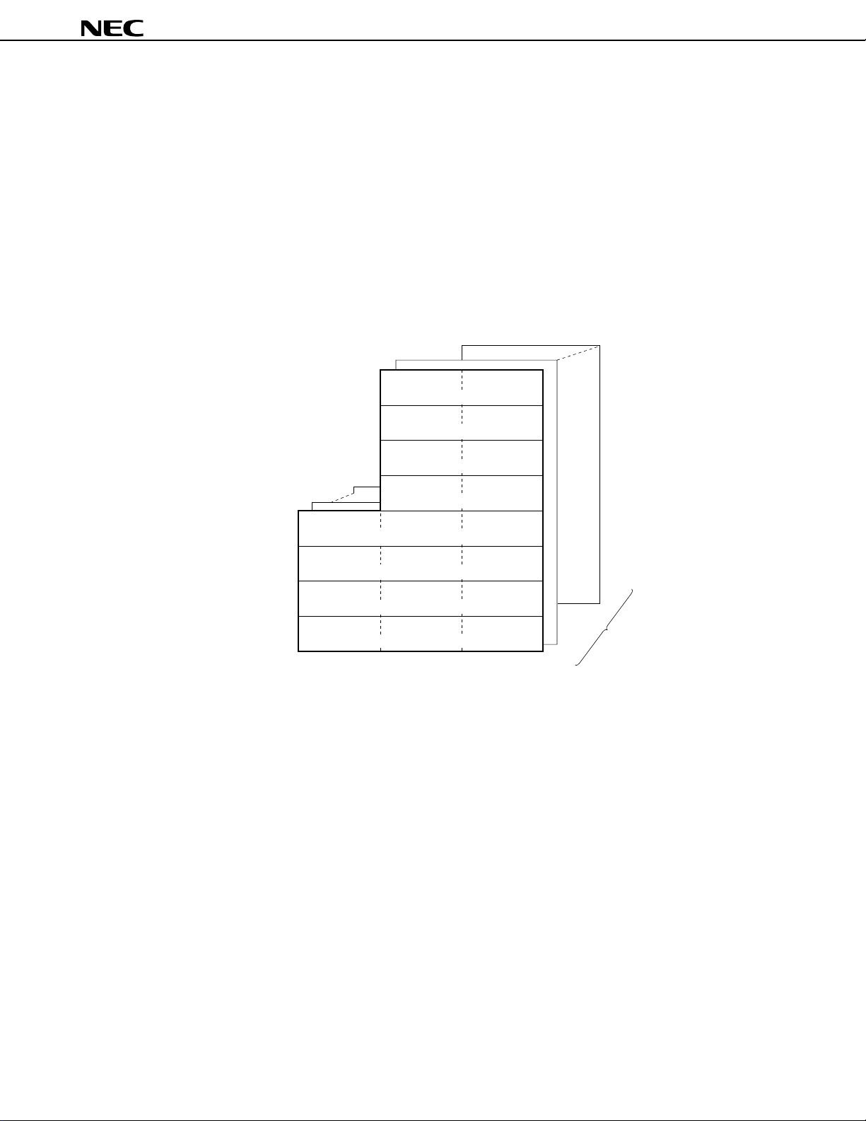
APPENDIX B RELATED DOCUMENTS ......................................................................................... 94
7Data Sheet U11680EJ2V0DS00
Page 8
µ
PD784907, 784908
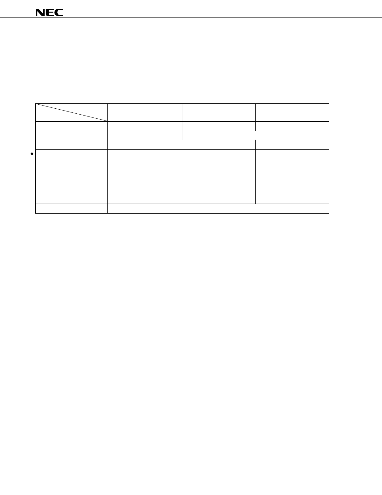
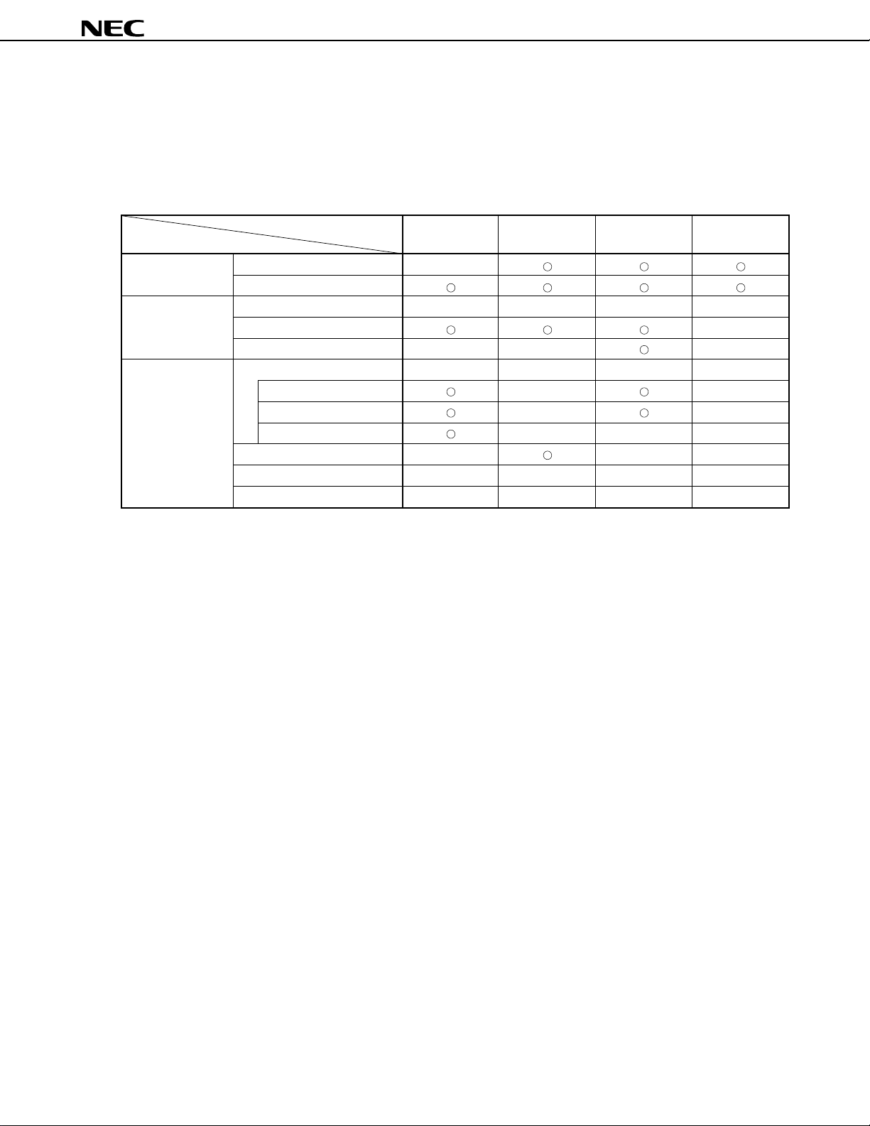
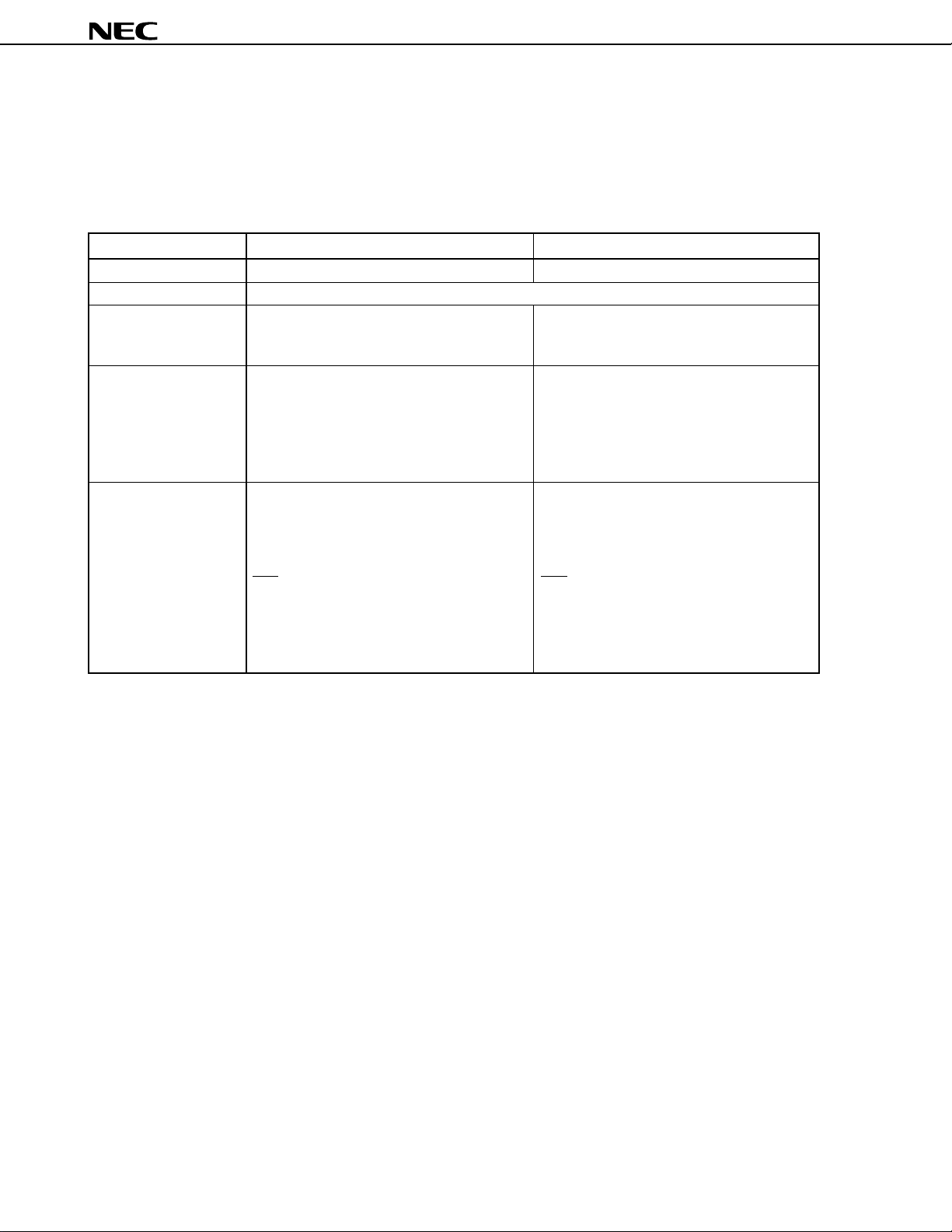
1. DIFFERENCES BETWEEN µPD784908 SUBSERIES PRODUCTS
The only difference between the µPD784907 and µPD784908 is their internal memory capacities.
The µPD78P4908 is produced by replacing the mask ROM in the µPD784907 or µPD784908 with 128-Kbyte one-
time PROM. Table 1-1 shows the differences between these products.
µ
Table 1-1. Differences between the
PD784908 Subseries Products
Part Number
Item
Internal ROM 96 K (mask ROM) 128 K (mask ROM) 128 K (one-time PROM)
Internal RAM 3,584 bytes 4,352 bytes
Regulator Provided None
Power supply voltage VDD = 4.0 to 5.5 V VDD = 4.5 to 5.5 V
(Main clock: fXX = 12.58 MHz, internal system clock = fXX, (Main clock: fXX = 12.58 MHz,
fCYK = 79 ns) internal system clock = fXX,
VDD = 3.5 to 5.5 V fCYK = 79 ns)
(other than above, fCYK = 159 ns) VDD = 4.0 to 5.5 V
Electrical specifications Refer to the data sheet of each product.
µ
PD784907
µ
PD784908
µ
PD78P4908
(other than above,
fCYK = 159 ns)
8
Data Sheet U11680EJ2V0DS00
Page 9
µ
PD784907, 784908
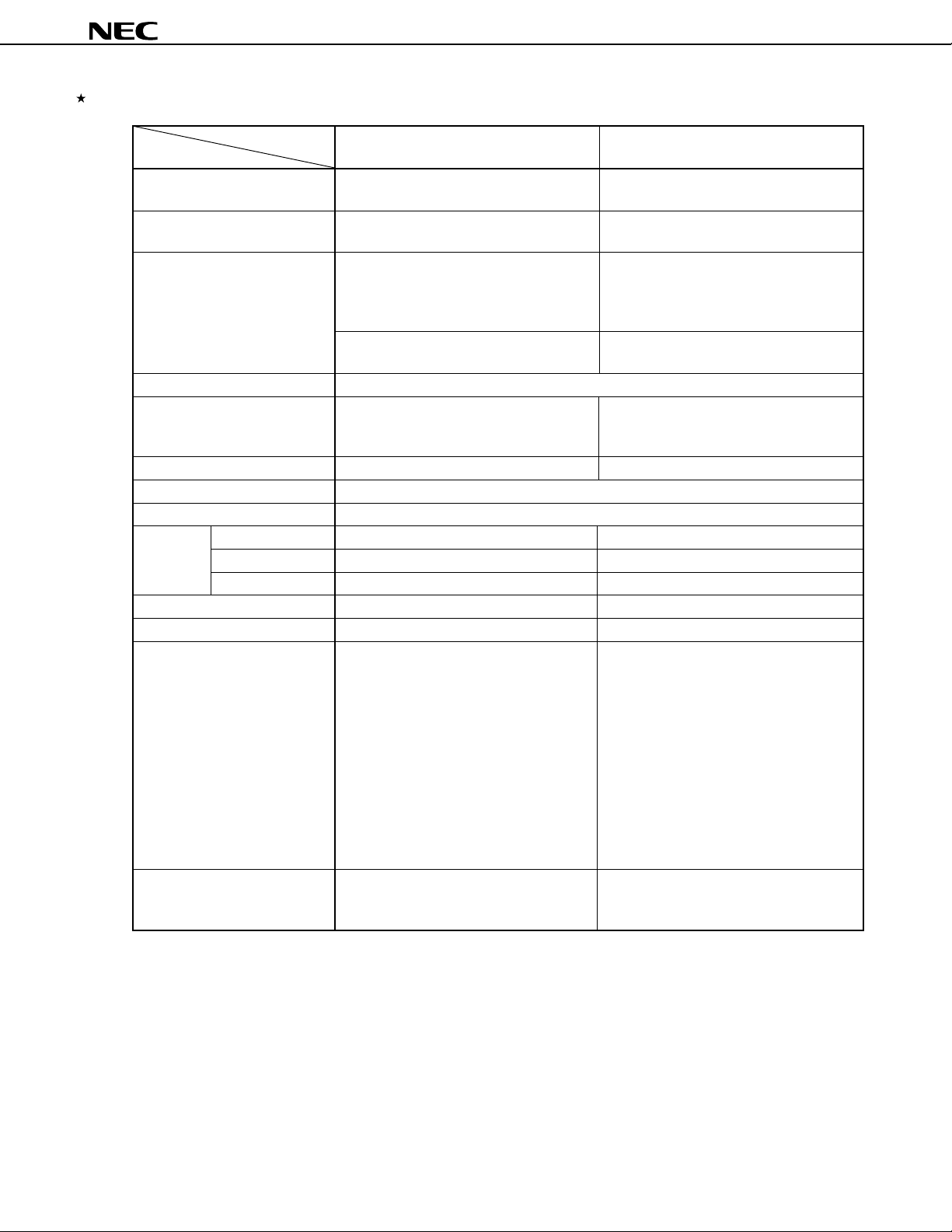
2. MAJOR DIFFERENCES BETWEEN µPD784908 AND µPD78098 SUBSERIES
Series Name
Item
Number of basic instructions 113 63
(mnemonics)
Minimum instruction execution 320/160 ns 480 ns
time (at 6.29/12.58 MHz operation) (at 6.29 MHz operation)
Timer/counter 16-bit timer/counter × 1 16-bit timer/counter × 1
8/16-bit timer/counter × 2 8/16-bit timer/counter × 2
8/16-bit timer × 1 Watch timer
Watch timer
Single clock Dual clock
Watch clock for clock operation
Watchdog timer Provided
Serial interface UART/IOE (3-wire serial I/O): 2 channels UART (3-wire serial I/O): 1 channel
CSI (3-wire serial I/O): 2 channels CSI/SBI (3-wire serial I/O): 1 channel
PWM output 2 None
A/D converter 8-bit resolution × 8 channels
D/A converter None
Interrupt Hardware source 27 23 (two test flags)
Internal 20 14
External 7 7
External extended function Provided (up to 1 Mbyte) None
IEBus controller Incorporated (simplified) Incorporated (complete hardware)
Power supply voltage • Mask ROM version VDD = 2.7 to 6.0 V
VDD = 4.0 to 5.5 V
(Main clock: fXX = 12.58 MHz,
internal system clock = fXX, fCYK = 79 ns)
VDD = 3.5 to 5.5 V
(other than above, fCYK = 159 ns)
• PROM version
VDD = 4.5 to 5.5 V
(Main clock: fXX = 12.58 MHz,
internal system clock = fXX, fCYK = 79 ns)
VDD = 4.0 to 5.5 V
(other than above, fCYK = 159 ns)
Package 100-pin plastic QFP (14 × 20 mm) 80-pin plastic QFP (14 × 14 mm)
µ
PD784908 Subseries
µ
PD78098 Subseries
CSI (3-wire serial I/O): 1 channel
80-pin plastic WQFN (14 × 14 mm):
µ
PD78P098A only
9Data Sheet U11680EJ2V0DS00
Page 10
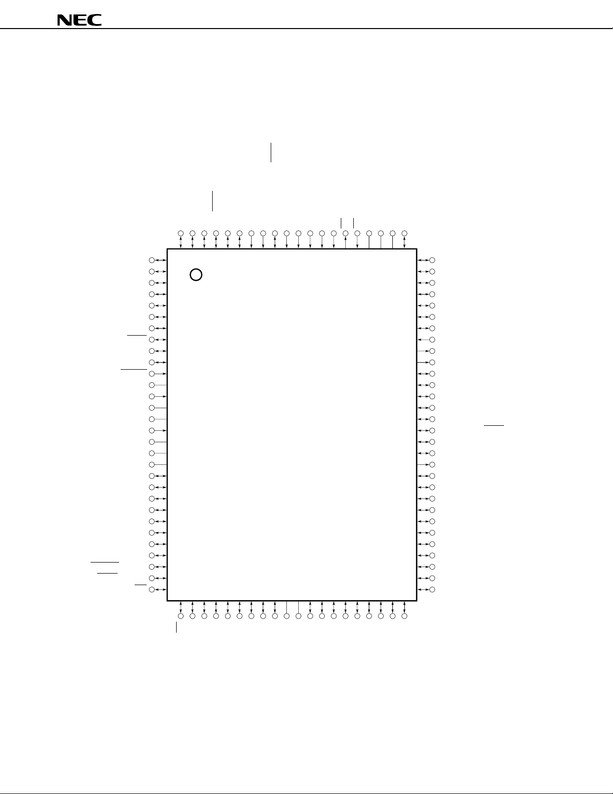
3. PIN CONFIGURATION (TOP VIEW)
• 100-pin plastic QFP (14 × 20 mm)
µ
PD784907GF-×××-3BA
µ
PD784908GF-×××-3BA
P35/TO1
P34/TO099P33/SO0
P32/SCK0
P31/TxD/SO1
100
98
97
96
2P37/TO3
3P100
4P101
5P102
6P103
7P104
8P105/SCK3
9P106/SI3
10P107/SO3
11RESET
12XT2
13XT1
14V
SS
15X2
Note 2
Note 3
16X1
17REGOFF
18REGC
19VDD
20P00
21P01
22P02
23P03
24P04
25P05
26P06
27P07
28P67/REFRQ/HLDAK
29P66/WAIT/HLDRQ
30P65/WR
31 32 33 34 35 36 37 38 39 40 41 42 43 44 45 46 47 48 49 50
P30/RxD/SI1
P27/SI094P26/INTP5
95
93
P25/INTP4/ASCK/SCK1
P24/INTP3
P23/INTP2/CI
P22/INTP1
P21/INTP0
P20/NMI87TX86RX85AVSS84AVREF183AVDD82P77/ANI7
92
91
90
89
88
µ
PD784907, 784908
81
80 P76/ANI61P36/TO2
79 P75/ANI5
78 P74/ANI4
77 P73/ANI3
76 P72/ANI2
75 P71/ANI1
74 P70/ANI0
73 TEST
72 PWM1
71 PWM0
70 P17
69 P16
68 P15
67 P14/TxD2/SO2
66 P13/RxD2/SI2
65 P12/ASCK2/SCK2
64 P11
63 P10
62 ASTB/CLKOUT
61 P90
60 P91
59 P92
58 P93
57 P94
56 P95
55 P96
54 P97
53 P40/AD0
52 P41/AD1
51 P42/AD2
Note 1
P64/RD
P63/A19
P62/A18
P61/A17
Notes 1. Connect the TEST pin directly to V
2. Connect the REGOFF pin directly to VSS (select regulator operation).
3. Connect the REGC pin to V
10
SS
V
VDD
P51/A9
P60/A16
P57/A15
P56/A14
P55/A13
P54/A12
SS.
SS via a capacitor of the order of 1
Data Sheet U11680EJ2V0DS00
P53/A11
P52/A10
P50/A8
P47/AD7
P46/AD6
P45/AD5
P44/AD4
µ
F.
P43/AD3
Page 11

µ
PD784907, 784908
A8 to A19: Address bus
AD0 to AD7: Address/data bus
ANI0 to ANI7: Analog input
ASCK, ASCK2: Asynchronous serial clock
ASTB: Address strobe
DD: Analog power supply
AV
AVREF1: Reference voltage
AVSS: Analog ground
CI: Clock input
CLKOUT: Clock output
HLDAK: Hold acknowledge
HLDRQ: Hold request
INTP0 to INTP5: Interrupt from peripherals
NMI: Non-maskable interrupt
P00 to P07: Port 0
P10 to P17: Port 1
P20 to P27: Port 2
P30 to P37: Port 3
P40 to P47: Port 4
P50 to P57: Port 5
P60 to P67: Port 6
P70 to P77: Port 7
P90 to P97: Port 9
P100 to P107: Port 10
PWM0, PWM1: Pulse width modulation output
RD: Read strobe
REFRQ: Refresh request
REGC: Regulator capacitance
REGOFF: Regulator off
RESET: Reset
RX: IEBus receive data
XD, RXD2: Receive data
R
SCK0 to SCK3: Serial clock
SI0 to SI3: Serial input
SO0 to SO3: Serial output
TEST: Test
TO0 to TO3: Timer output
TX: IEBus transmit data
XD, TXD2: Transmit data
T
VDD: Power supply
VSS: Ground
WAIT: Wait
WR: Write strobe
X1, X2: Crystal (main system clock)
XT1, XT2: Crystal (watch)
11Data Sheet U11680EJ2V0DS00
Page 12
µ
PD784907, 784908
4. SYSTEM CONFIGURATION EXAMPLE (AUTOMOTIVE CAR AUDIO (TUNER DECK))
Front panel PD784908
Remote-controll
FIP
µ
TM
FIP
controller/driver
µ
signal reception
circuit
PC2800A, etc.
Key
matrix
PD16312, etc.
Interrupt input
SIO with automatic
transmission/reception
function
LED
display
Audio control
circuit
Electronic
volume
EEPROM
TM
3-wire serial I/O
µ
General-purpose
port
3-wire serial I/O
IEBus controller
REGOFF
REGC
Cassette deck
unit
Tuner pack
IEBus
driver/
receiver
IEBus
CD unit
CD changer,
one CD, etc.
DSP unit
TV unit
12
Data Sheet U11680EJ2V0DS00
Page 13
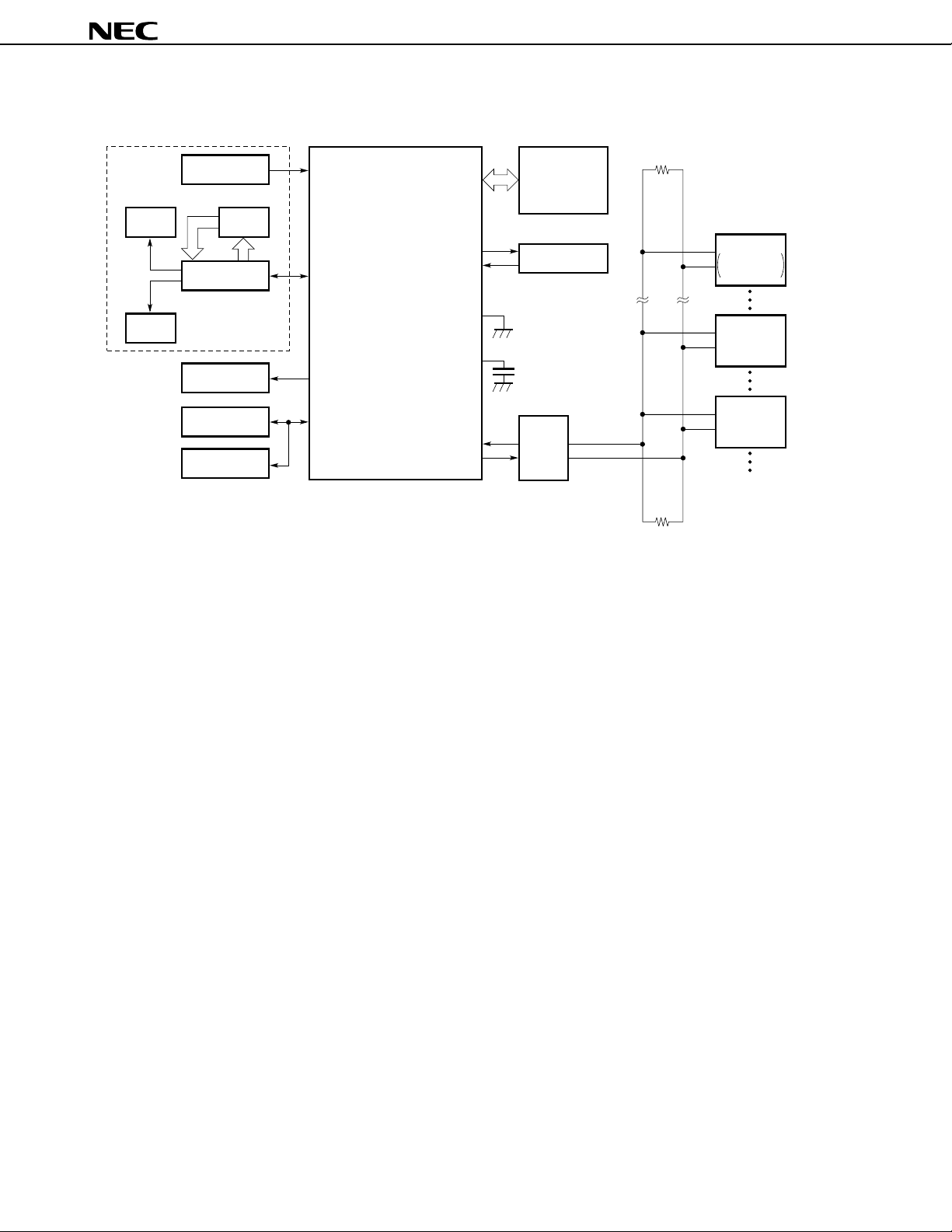
5. BLOCK DIAGRAM
µ
PD784907, 784908
NMI
INTP0 to INTP5
INTP3
TO0
TO1
INTP0
INTP1
INTP2/CI
TO2
TO3
P00 to P03
P04 to P07
PWM0
PWM1
Programmable
interrupt controller
Timer/counter 0
(16 bits)
Timer/counter 1
(16 bits)
Timer/counter 2
(16 bits)
Timer 3
(16 bits)
Real-time output
port
PWM
78K/IV
CPU core
RAM
ROM
UART/IOE2
Baud-rate
generator
UART/IOE1
Baud-rate
generator
Clocked serial
interface
Clocked serial
interface 3
Clock output
Bus interface
RxD/SI1
TxD/SO1
ASCK/SCK1
RxD2/SI2
TxD2/SO2
ASCK2/SCK2
SCK0
SO0
SI0
SCK3
SO3
SI3
ASTB/CLKOUT
AD0 to AD7
A8 to A15
A16 to A19
RD
WR
WAIT/HLDRQ
REFRQ/HLDAK
ANI0 to ANI7
AV
DD
AV
REF1
AV
INTP5
TX
RX
RESET
TEST
X1
X2
REGC
REGOFF
V
V
XT1
XT2
SS
DD
SS
A/D converter
IEBus controller
System control
(regulator)
Watch timer
Watchdog timer
Remark The internal ROM and RAM capacities differ depending on the product.
Port 0
Port 1
Port 2
Port 3
Port 4
Port 5
Port 6
Port 7
Port 9
Port 10
P00 to P07
P10 to P17
P20 to P27
P30 to P37
P40 to P47
P50 to P57
P60 to P67
P70 to P77
P90 to P97
P100 to P107
13Data Sheet U11680EJ2V0DS00
Page 14
6. PIN FUNCTIONS
6.1 Port Pins (1/2)
Pin Name I/O Alternate Function Function
P00 to P07 I/O — Port 0 (P0):
• 8-bit I/O port.
• Can be used as a real-time output port (4 bits × 2).
• Input and output can be specified by 1-bit units.
• The use of on-chip pull-up resistors can be simultaneously specified by
software for all pins in input mode.
• Can drive transistors.
P10 I/O —
P11 —
P12 ASCK2/SCK2
P13 RxD2/SI2
P14 TxD2/SO2
P15 to P17 —
P20 Input NMI
P21 INTP0
P22 INTP1
P23 INTP2/CI
P24 INTP3
P25 INTP4/ASCK/SCK1
P26 INTP5
P27 SI0
P30 I/O RxD/SI1
P31 TxD/SO1
P32 SCK0
P33 SO0
P34 to P37 TO0 to TO3
P40 to P47 I/O AD0 to AD7 Port 4 (P4):
P50 to P57 I/O A8 to A15 Port 5 (P5):
Port 1 (P1):
• 8-bit I/O port.
• Input and output can be specified in 1-bit units.
• The use of on-chip pull-up resistors can be simultaneously specified by
software for all pins in input mode.
• Can drive LEDs.
Port 2 (P2):
• 8-bit input port.
• P20 does not function as a general-purpose port (non-maskable interrupt).
However, the input level can be checked by an interrupt service routine.
• The use of on-chip pull-up resistors can be specified by software for pins
P22 to P27 (in 6-bit units).
• The P25/INTP4/ASCK/SCK1 pin functions as the SCK1 output pin by a
CSIM1 specification.
Port 3 (P3):
• 8-bit I/O port.
• Input and output can be specified in 1-bit units.
• The use of on-chip pull-up resistors can be simultaneously specified by
software for all pins in input mode.
• The use of the N-ch open drain can be specified for pins P32 and P33.
• 8-bit I/O port.
• Input and output can be specified in 1-bit units.
• The use of on-chip pull-up resistors can be simultaneously specified by
software for all pins in input mode.
• Can drive LEDs.
• 8-bit I/O port.
• Input and output can be specified in 1-bit units.
• The use of on-chip pull-up resistors can be simultaneously specified by
software for all pins in input mode.
• Can drive LEDs.
µ
PD784907, 784908
14
Data Sheet U11680EJ2V0DS00
Page 15
6.1 Port Pins (2/2)
Pin Name I/O Alternate Function Function
P60 to P63 I/O A16 to A19
P64 RD
P65 WR
P66 WAIT/HLDRQ
P67 REFRQ/HLDAK
P70 to P77 I/O ANI0 to ANI7 Port 7 (P7):
P90 to P97 I/O — Port 9 (P9):
P100 to I/O —
P104
P105 SCK3
P106 SI3
P107 SO3
Port 6 (P6):
• 8-bit I/O port.
• Input and output can be specified in 1-bit units.
• The use of on-chip pull-up resistors can be simultaneously specified by
software for all pins in input mode.
• 8-bit I/O port.
• Input and output can be specified in 1-bit units.
• 8-bit I/O port.
• Input and output can be specified in 1-bit units.
• The use of on-chip pull-up resistors can be simultaneously specified by
software for all pins in input mode.
Port 10 (P10):
• 8-bit I/O port.
• Input and output can be specified in 1-bit units.
• The use of on-chip pull-up resistors can be simultaneously specified by
software for all pins in input mode.
• The use of the N-ch open drain can be specified for pins P105 and P107.
µ
PD784907, 784908
15Data Sheet U11680EJ2V0DS00
Page 16
µ
PD784907, 784908
6.2 Non-Port Pins (1/2)
Pin Name I/O Alternate Function Function
TO0 to TO3 Output P34 to P37 Timer output
CI Input P23/INTP2 Input of a count clock for timer/counter 2
RxD Input P30/SI1 Serial data input (UART0)
RxD2 P13/SI2 Serial data input (UART2)
TxD Output P31/SO1 Serial data output (UART0)
TxD2 P14/SO2 Serial data output (UART2)
ASCK Input P25/INTP4/SCK1 Baud rate clock input (UART0)
ASCK2 P12/SCK2 Baud rate clock input (UART2)
SI0 Input P27 Serial data input (3-wire serial I/O 0)
SI1 P30/RxD Serial data input (3-wire serial I/O 1)
SI2 P13/RxD2 Serial data input (3-wire serial I/O 2)
SI3 P106 Serial data input (3-wire serial I/O 3)
SO0 Output P33 Serial data output (3-wire serial I/O 0)
SO1 P31/TxD Serial data output (3-wire serial I/O 1)
SO2 P14/TxD2 Serial data output (3-wire serial I/O 2)
SO3 P107 Serial data output (3-wire serial I/O 3)
SCK0 I/O P32 Serial clock I/O (3-wire serial I/O 0)
SCK1 P25/INTP4/ASCK Serial clock I/O (3-wire serial I/O 1)
SCK2 P12/ASCK2 Serial clock I/O (3-wire serial I/O 2)
SCK3 P105 Serial clock I/O (3-wire serial I/O 3)
NMI Input P20 External interrupt —
INTP0 P21 request • Input of a count clock for timer/counter 1
• Capture/trigger signal for CR11 or CR12
INTP1 P22 • Input of a count clock for timer/counter 2
• Capture/trigger signal for CR22
INTP2 P23/CI • Input of a count clock for timer/counter 2
• Capture/trigger signal for CR21
INTP3 P24 • Input of a count clock for timer/counter 0
• Capture/trigger signal for CR02
INTP4 P25/ASCK/SCK1 —
INTP5 P26
AD0 to AD7 I/O P40 to P47 Time multiplexing address/data bus (for connecting external memory)
A8 to A15 Output P50 to P57 High-order address bus (for connecting external memory)
A16 to A19 Output P60 to P63 High-order address bus during address expansion (for connecting external
memory)
RD Output P64 Strobe signal output for reading the contents of external memory
WR Output P65 Strobe signal output for writing on external memory
WAIT Input P66/HLDRQ Wait insertion
REFRQ Output P67/HLDAK Refresh pulse output to external pseudo static memory
HLDRQ Input P66/WAIT Input of bus hold request
HLDAK Output P67/REFRQ Output of bus hold response
ASTB Output CLKOUT Latch timing output of time multiplexing address (A0 to A7) (for connecting
external memory)
Input of a conversion start trigger for A/D converter
16
Data Sheet U11680EJ2V0DS00
Page 17
µ
PD784907, 784908
6.2 Non-Port Pins (2/2)
Pin Name I/O Alternate Function Function
CLKOUT Output ASTB Clock output
PWM0 Output — PWM output 0
PWM1 Output — PWM output 1
RX Input — Data input (IEBus)
TX Output — Data output (IEBus)
REGC — — Capacitance connection for stabilizing the regulator output/power supply
when the regulator is stopped. Connect to VSS via a capacitor of order of 1µF.
REGOFF — — Signal for specifying regulator operation
RESET Input — Chip reset
X1 Input — Crystal input for system clock oscillation (A clock pulse can also be input
X2 —
XT1 Input — Watch clock connection
XT2 — —
ANI0 to ANI7 Input P70 to P77 Analog voltage input for A/D converter
AVREF1 — — To apply the reference voltage for A/D converter
AVDD Positive power supply for A/D converter
AVSS GND for A/D converter
VDD Positive power supply
VSS GND
TEST Input Connect directly to V
to the X1 pin.)
SS. (This pin is for IC test.)
Data Sheet U11680EJ2V0DS00
17
Page 18
µ
PD784907, 784908
6.3 Pin I/O Circuits and Recommended Connections of Unused Pins
The input/output circuit type of each pin and recommended connections of unused pins are shown in Table 6-1.
For each type of input/output circuit, refer to Figure 6-1.
Table 6-1. Types of Pin I/O Circuits and Recommended Connections of Unused Pins (1/2)
Pin Name I/O Circuit Type I/O Recommended Connections of Unused Pins
P00 to P07 5-A I/O Input: Connect to VDD
P10, P11
P12/ASCK2/SCK2 8-A
P13/RxD2/SI2 5-A
P14/TxD2/SO2
P15 to P17
P20/NMI 2 Input Connect to VDD or VSS
P21/INTP0
P22/INTP1 2-A Connect to VDD
P23/INTP2/CI
P24/INTP3
P25/INTP4/ASCK/SCK1 8-A I/O Input: Connect to VDD
P26/INTP5 2-A Input Connect to VDD
P27/SI0
P30/RxD/SI1 5-A I/O Input: Connect to VDD
P31/TxD/SO1
P32/SCK0 10-A
P33/SO0
P34/TO0 to P37/TO3 5-A
P40/AD0 to P47/AD7
P50/A8 to P57/A15
P60/A16 to P63/A19
P64/RD
P65/WR
P66/WAIT/HLDRQ
P67/REFRQ/HLDAK
P70/ANI0 to P77/ANI7 20 I/O Input: Connect to VDD or VSS
P90 to P97 5-A
P100 to P104
P105/SCK3 10-A
P106/SI3 8-A
P107/SO3 10-A
ASTB/CLKOUT 4 Output Leave open
Output:Leave open
Output:Leave open
Output:Leave open
Output:Leave open
18
Data Sheet U11680EJ2V0DS00
Page 19
µ
PD784907, 784908
Table 6-1. Types of Pin I/O Circuits and Recommended Connections of Unused Pins (2/2)
Pin Name I/O Circuit Type I/O Recommended Connections of Unused Pins
RESET 2 Input —
TEST 1 Connect directly to VSS
XT2 — — Leave open
XT1 — Input Connect to V SS
PWM0, PWM1 3 Output Leave open
RX 1 Input Connect to VDD or VSS
TX 3 Output Leave open
AVREF1 — — Connect to VSS
AVSS
AVDD Connect to VDD
Caution Connect an I/O pin, whose input/output mode is undefined, to VDD via a resistor of several
10 kΩ (especially if the voltage on the reset input pin rises higher than the low level input at power
on or when the mode is being switched between input and output by software).
Remark Since type numbers are commonly used in the 78K Series, these numbers are not always serial in each
product (some circuits are not included).
Data Sheet U11680EJ2V0DS00
19
Page 20
Figure 6-1. I/O Circuits for Pins
Type 1 Type 4
DD
V
P
Data
µ
PD784907, 784908
V
DD
P
OUT
IN
N
Push-pull output which can output high impedance
(both the positive and negative channels are off.)
Type 2
Type 5-A
Pull-up
enable
IN
Schmitt trigger input with hysteresis characteristics
Data
Output
disable
Input
enable
Type 2-A Type 8-A
V
DD
Output
disable
N
V
DD
P
DD
V
P
IN/OUT
N
V
DD
Pull-up
P
Pull-up
enable
enable
Data
IN
Output
disable
Schmitt trigger input with hysteresis characteristics
Type 3 Type 10-A
DD
V
Pull-up
enable
P-ch
Data
Data OUT
Open
N-ch
drain
Output
disable
V
DD
P
IN/OUT
N
P
V
DD
P
V
DD
P
IN/OUT
N
20
Data Sheet U11680EJ2V0DS00
Page 21
Type 20
µ
PD784907, 784908
V
DD
Output
disable
Input
enable
Data
Comparator
(Threshold voltage)
P
IN/OUT
N
+
–
V
REF
P
N
Data Sheet U11680EJ2V0DS00
21
Page 22
µ
PD784907, 784908
7. CPU ARCHITECTURE
7.1 Memory Space
A memory space of 1 Mbyte can be accessed. By using a LOCATION instruction, the mode for mapping internal
data areas (special function registers and internal RAM) can be selected. A LOCATION instruction must always be
executed after a reset, and can be used only once.
(1) When the LOCATION 0 instruction is executed
• Internal memory
The internal data area and internal ROM area are mapped as follows:
Part Number Internal Data Area Internal ROM Area
µ
PD784907 0F100H to 0FFFFH 00000H to 0F0FFH
10000H to 17FFFH
µ
PD784908 0EE00H to 0FFFFH 00000H to 0FDFFH
10000H to 1FFFFH
Caution The following internal ROM areas, existing at the same addresses as the internal data areas,
cannot be used when the LOCATION 0 instruction is executed:
Part Number Unusable Area
µ
PD784907 0F100H to 0FFFFH (3,840 bytes)
µ
PD784908 0EE00H to 0FFFFH (4,608 bytes)
• External memory
The external memory is accessed in external memory expansion mode.
(2) When the LOCATION 0FH instruction is executed
• Internal memory
The internal data area and internal ROM area are mapped as follows:
Part Number Internal Data Area Internal ROM Area
µ
PD784907 FF100H to FFFFFH 00000H to 17FFFH
µ
PD784908 FEE00H to FFFFFH 00000H to 1FFFFH
• External memory
The external memory is accessed in external memory expansion mode.
22
Data Sheet U11680EJ2V0DS00
Page 23
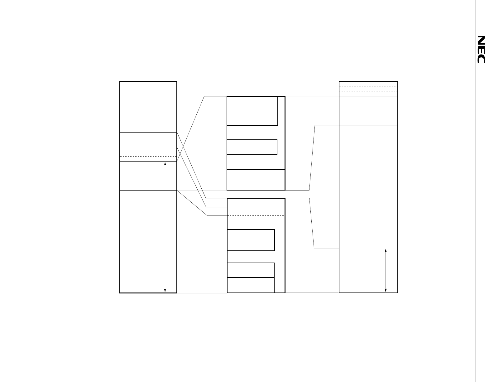
Figure 7-1.
µ
PD784907 Memory Map
Data Sheet U11680EJ2V0DS00
FFFFFH
18000H
1 7FFFH
10000H
0FFFFH
0 FFDFH
0 FFD0H
0FF00H
0FEFFH
0F100H
0F0FFH
00000H
When the LOCATION 0
instruction is executed
External memory
(928 Kbytes)
Note 1
Internal ROM
(32,768 bytes)
Special function registers (SFRs)
Note 1
(256 bytes)
Internal RAM
(3,584 bytes)
Internal ROM
(61,696 bytes)
Note 4
0FEFFH
0FE80H
0FE7FH
0FE39H
0FE06H
0 FD0 0H
0 FCFFH
0F100H
17FFFH
10000H
0F0FFH
01000H
0 0FFFH
00800H
007FFH
00080H
0007FH
00040H
0003FH
00000H
General-purpose
registers (128 bytes)
Macro service control
word area (42 bytes)
Data area (512 bytes)
Program/data area
(3,072 bytes)
Note 2
Program/data area
CALLF entry area
(2 Kbytes)
CALLT table area
(64 bytes)
Vector table area
(64 bytes)
Note 3
FFEFFH
FFE80H
FFE7FH
FFE39H
FFE06H
FFD00H
F FCFFH
FF100H
1 7FFFH
FFFFFH
FFFDFH
FFFD0H
FFF00H
FFEFFH
FF100H
FF0FFH
18000H
1 7FFFH
00000H
When the LOCATION 0FH
instruction is executed
Special function registers (SFRs)
Note 1
(256 bytes)
Internal RAM
(3,584 bytes)
External memory
(946,432 bytes)
Internal ROM
(96 Kbytes)
Note 1
Note 4
µ
PD784907, 784908
23
Notes 1. Accessed in external memory expansion mode.
2. This 3,840-byte area can be used as an internal ROM area only when the LOCATION 0FH instruction is executed.
3. When the LOCATION 0 instruction is executed: 94,464 bytes
When the LOCATION 0FH instruction is executed: 98,304 bytes
4. Base area and entry area based on a reset or interrupt. However, internal RAM is not used as a reset entry area.
Page 24
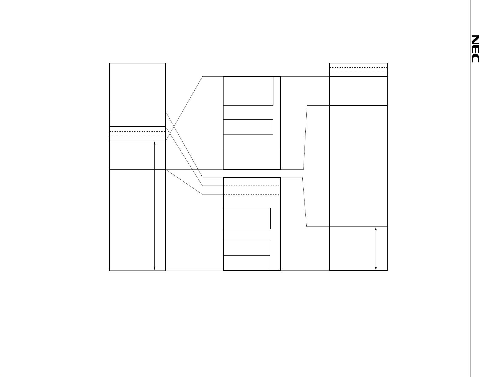
24
Figure 7-2.
µ
PD784908 Memory Map
Data Sheet U11680EJ2V0DS00
FFFFFH
20000H
1FFFFH
10000H
0FFFFH
0FFDFH
0FFD0H
0FF 00H
0FEFFH
0EE00H
0EDFFH
00000H
When the LOCATION 0
instruction is executed
External memory
(896 Kbytes)
Note 1
Internal ROM
(65,536 bytes)
Special function registers (SFRs)
Note 1
(256 bytes)
Internal RAM
(4,352 bytes)
Internal ROM
(60,928 bytes)
Note 4
0FEFFH
0FE8 0H
0FE7 FH
0FE3 9H
0FE0 6H
0FD00H
0FCFFH
0EE00H
1FFFFH
10000H
0EDFFH
01000H
00FFFH
00800H
007 FFH
00080H
0007FH
00040H
0003FH
00000H
General-purpose
registers (128 bytes)
Macro service control
word area (42 bytes)
Data area (512 bytes)
Program/data area
(3,840 bytes)
Note 2
Program/data area
CALLF entry area
(2 Kbytes)
CALLT table area
(64 bytes)
Vector table area
(64 bytes)
Note 3
FFEFFH
FFE 8 0H
FFE 7 FH
FFE 3 9H
FFE 0 6H
FFD00H
FFCFFH
FEE 0 0 H
1FFFFH
FFFFFH
FFFDFH
FFFD0H
FFF00H
FFEFFH
FEE 0 0 H
FEDFFH
20000H
1FFFFH
00000H
When the LOCATION 0FH
instruction is executed
Special function registers (SFRs)
Note 1
(256 bytes)
Internal RAM
(4,352 bytes)
External memory
(912,896 bytes)
Internal ROM
(128 Kbytes)
Note 1
Note 4
µ
PD784907, 784908
Notes 1. Accessed in external memory expansion mode.
2. This 4,608-byte area can be used as an internal ROM area only when the LOCATION 0FH instruction is executed.
3. When the LOCATION 0 instruction is executed: 126,464 bytes
When the LOCATION 0FH instruction is executed: 131,072 bytes
4. Base area and entry area based on a reset or interrupt. However, internal RAM is not used as a reset entry area.
Page 25
µ
PD784907, 784908
7.2 CPU Registers
7.2.1 General-purpose registers
A set of general-purpose registers consists of sixteen 8-bit general-purpose registers. Two 8-bit general-purpose
registers can be combined to form a 16-bit general-purpose register. Moreover, four 16-bit general-purpose registers,
when combined with an 8-bit register for address extension, can be used as 24-bit address specification registers.
Eight banks of this register set are provided. The user can switch between banks by software or the context switching
function.
General-purpose registers other than the V, U, T, and W registers used for address extension are mapped onto
internal RAM.
Figure 7-3. General-Purpose Register Format
A (R1) X (R0)
AX (RP0)
B (R3) C (R2)
BC (RP1)
R5 R4
RP2
R7 R6
RP3
V
VVP (RG4)
U
UUP (RG5)
T
TDE (RG6)
W L (R14)
WHL (RG7)
The character strings enclosed in
parentheses represent absolute names.
R9 R8
VP (RP4)
R11 R10
UP (RP5)
D (R13) E (R12)
DE (RP6)
H (R15)
HL (RP7)
8 banks
Caution By setting the RSS bit of PSW to 1, R4, R5, R6, R7, RP2, and RP3 can be used as the X, A, C,
B, AX, and BC registers, respectively. However, this function must be used only when using
programs for the 78K/III series.
Data Sheet U11680EJ2V0DS00
25
Page 26
µ
PD784907, 784908
7.2.2 Control registers
(1) Program counter (PC)
This register is a 20-bit program counter. The program counter is automatically updated by program execution.
Figure 7-4. Format of Program Counter (PC)
19 0
PC
(2) Program Status Word (PSW)
This register holds the CPU state. The program status word is automatically updated by program execution.
Figure 7-5. Format of Program Status Word (PSW)
PSW
PSWH
PSWL
15 14 13 12
UF RBS2 RBS1 RBS0
76543210
S Z RSS
Note
AC IE P/V 0 CY
11 10 9 8
Note This flag is used to maintain compatibility with the 78K/III Series. This flag must be set to 0 when
programs for the 78K/III Series are not being used.
(3) Stack pointer (SP)
This register is a 24-bit pointer for holding the start address of the stack.
The higher 4 bits must be set to 0.
Figure 7-6. Format of Stack Pointer (SP)
23 20 0
SP 0 0 0 0
26
Data Sheet U11680EJ2V0DS00
Page 27

µ
PD784907, 784908
7.2.3 Special function registers (SFRs)
The special function registers are registers with special functions such as mode registers and control registers for
built-in peripheral hardware. The special function registers are mapped onto the 256-byte space between 0FF00H
Note
and 0FFFFH
Note On execution of the LOCATION 0 instruction. FFF00H to FFFFFH when the LOCATION 0FH instruction
Caution Do not access an address in this area where no SFR is allocated, as the
Table 7-1 lists the special function registers (SFRs). The symbols of the table columns are explained below.
• Symbol.................................... Symbol indicating an on-chip SFR. The symbols listed in the table are reserved
• R/W ......................................... Indicates whether the SFR is read-only, write-only, or read/write.
• Bit units for manipulation ....... Indicates the maximum number of bits that can be manipulated whenever an SFR
• After reset............................... Indicates the state of the register when the RESET signal has been input.
.
is executed.
in the deadlock state. The deadlock state can be cleared only by a reset.
words for the NEC assembler (RA78K4). In the C compiler (CC78K4), the
symbols can be used as sfr variables with the #pragma sfr command.
R/W: Read/write
R: Read-only.
W: Write-only.
is manipulated. An SFR that supports 16-bit manipulation can be described in
the sfrp operand. For address specification, an even-numbered address must
be specified.
An SFR that can be manipulated in 1-bit units can be described as the operand
of a bit manipulation instruction.
µ
PD784908 may be placed
Data Sheet U11680EJ2V0DS00
27
Page 28
Table 7-1. Special Function Registers (SFRs) (1/5)
µ
PD784907, 784908
Address
0FF00H Port 0 P0 R/W — Undefined
0FF01H Port 1 P1 —
0FF02H Port 2 P2 R —
0FF03H Port 3 P3 R/W —
0FF04H Port 4 P4 —
0FF05H Port 5 P5 —
0FF06H Port 6 P6 — 00H
0FF07H Port 7 P7 — Undefined
0FF09H Port 9 P9 —
0FF0AH Port 10 P10 —
0FF0EH Port 0 buffer register L P0L —
0FF0FH Port 0 buffer register H P0H —
0FF10H Compare register (timer/counter 0) CR00 — —
0FF12H Capture/compare register (timer/counter 0) CR01 — —
0FF14H Compare register L (timer/counter 1) CR10
0FF15H Compare register H (timer/counter 1) — — —
0FF16H Capture/compare register L (timer/counter 1) CR11
0FF17H Capture/compare register H (timer/counter 1) — — —
0FF18H Compare register L (timer/counter 2) CR20
0FF19H Compare register H (timer/counter 2) — — —
0FF1AH Capture/compare register L (timer/counter 2) CR21
0FF1BH Capture/compare register H (timer/counter 2) — — —
0FF1CH Compare register L (timer 3) CR30
0FF1DH Compare register H (timer 3) — — —
0FF20H Port 0 mode register PM0 — FFH
0FF21H Port 1 mode register PM1 —
0FF23H Port 3 mode register PM3 —
0FF24H Port 4 mode register PM4 —
0FF25H Port 5 mode register PM5 —
0FF26H Port 6 mode register PM6 —
0FF27H Port 7 mode register PM7 —
0FF29H Port 9 mode register PM9 —
0FF2AH Port 10 mode register PM10 —
0FF2EH Real-time output port control register RTPC — 00H
0FF30H Capture/compare control register 0 CRC0 — — 10H
0FF31H Timer output control register TOC — 00H
0FF32H Capture/compare control register 1 CRC1 — —
0FF33H Capture/compare control register 2 CRC2 —
Note
Special Function Register (SFR) Name Symbol R/W
CR10W
CR11W
CR20W
CR21W
CR30W
Bit Units for Manipulation
1 bit 8 bits 16 bits
—
—
—
—
—
— 10H
After Reset
Note When the LOCATION 0 instruction is executed. When the LOCATION 0FH instruction is executed, F0000H
is added to each address.
28
Data Sheet U11680EJ2V0DS00
Page 29
µ
Table 7-1. Special Function Registers (SFRs) (2/5)
PD784907, 784908
Address
0FF36H Capture register (timer/counter 0) CR02 R — — 0000H
0FF38H Capture register L (timer/counter 1) CR12
0FF39H Capture register H (timer/counter 1) — — —
0FF3AH Capture register L (timer/counter 2) CR22
0FF3BH Capture register H (timer/counter 2) — — —
0FF41H Port 1 mode control register PMC1 R/W — 00H
0FF43H Port 3 mode control register PMC3 —
0FF4AH Port 10 mode control register PMC10 —
0FF4EH Register L for optional pull-up resistor PUOL —
0FF4FH Register H for optional pull-up resistor PUOH —
0FF50H Timer register 0 TM0 R — — 0000H
0FF51H ——
0FF52H Timer register 1 TM1 TM1W —
0FF53H — — —
0FF54H Timer register 2 TM2 TM2W —
0FF55H — — —
0FF56H Timer register 3 TM3 TM3W —
0FF57H — — —
0FF5CH Prescaler mode register 0 PRM0 R/W — — 11H
0FF5DH Timer control register 0 TMC0 — 00H
0FF5EH Prescaler mode register 1 PRM1 — — 11H
0FF5FH Timer control register 1 TMC1 — 00H
0FF68H A/D converter mode register ADM — 00H
0FF6AH A/D conversion result register ADCR R — — Undefined
0FF6CH A/D current cut selection register IEAD R/W — 00H
0FF6FH Clock timer mode register WM —
0FF70H PWM control register PWMC — 05H
0FF71H PWM prescaler register PWPR — — 00H
0FF72H PWM modulo register 0 PWM0 — — Undefined
0FF74H PWM modulo register 1 PWM1 — —
0FF7DH One-shot pulse output control register OSPC — 00H
0FF80H Clocked serial interface mode register 3 CSIM3 —
0FF82H Clocked serial interface mode register CSIM
Note
Special Function Register (SFR) Name Symbol R/W
CR12W
CR22W
Bit Units for Manipulation
1 bit 8 bits 16 bits
—
—
—
After Reset
Note When the LOCATION 0 instruction is executed. When the LOCATION 0FH instruction is executed, F0000H
is added to each address.
Data Sheet U11680EJ2V0DS00
29
Page 30
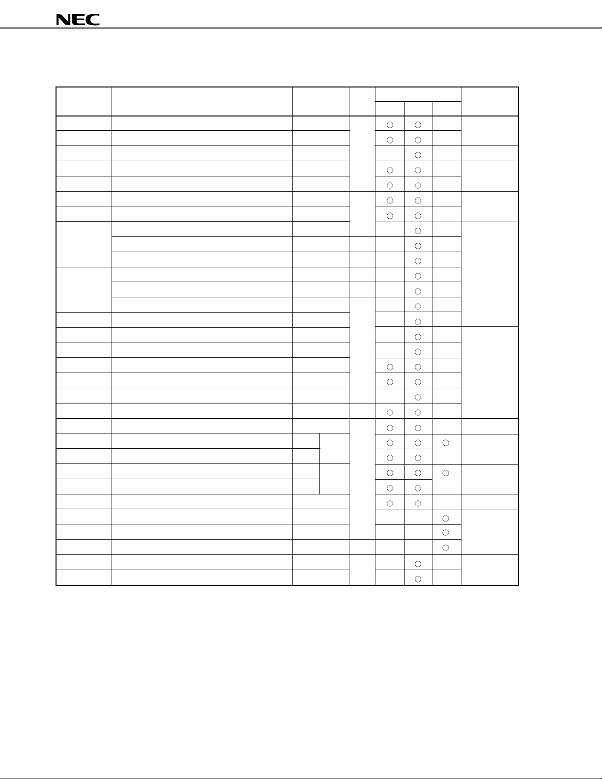
Table 7-1. Special Function Registers (SFRs) (3/5)
µ
PD784907, 784908
Address
0FF84H Clocked serial interface mode register 1 CSIM1 R/W — 00H
0FF85H Clocked serial interface mode register 2 CSIM2 —
0FF86H Serial shift register SIO — — Undefined
0FF88H Asynchronous serial interface mode register ASIM — 00H
0FF89H Asynchronous serial interface mode register 2 ASIM2 —
0FF8AH Asynchronous serial interface status register ASIS R —
0FF8BH Asynchronous serial interface status register 2 ASIS2 —
0FF8CH Serial receive buffer: UART0 RXB — — Undefined
0FF8DH Serial receive buffer: UART2 RXB2 R — —
0FF8EH Serial shift register 3: IOE3 SIO3 — —
0FF90H Baud rate generator control register BRGC — — 00H
0FF91H Baud rate generator control register 2 BRGC2 — —
0FFA0H External interrupt mode register 0 INTM0 —
0FFA1H External interrupt mode register 1 INTM1 —
0FFA4H Sampling clock selection register SCS0 — —
0FFA8H In-service priority register ISPR R —
0FFAAH Interrupt mode control register IMC R/W — 80H
0FFACH Interrupt mask register 0L MK0L MK0 FFFFH
0FFADH Interrupt mask register 0H MK0H
0FFAEH Interrupt mask register 1L MK1L MK1 FFFFH
0FFAFH Interrupt mask register 1H MK1H
0FFB0H Bus control register BCR — 00H
0FFB2H Unit address register UAR — — 0000H
0FFB4H Slave address register SAR — —
0FFB6H Partner address register PAR R — —
0FFB8H Control data register CDR R/W — — 01H
0FFB9H Telegraph length register DLR — —
Note
Special Function Register (SFR) Name Symbol R/W
Serial transmission shift register: UART0 TXS W — —
Serial shift register: IOE1 SIO1 R/W — —
Serial transmission shift register: UART2 TXS2 W — —
Serial shift register: IOE2 SIO2 R/W — —
Bit Units for Manipulation
1 bit 8 bits 16 bits
After Reset
Note Applicable when the LOCATION 0 instruction is executed. When the LOCATION 0FH instruction is executed,
F0000H is added to each address.
30
Data Sheet U11680EJ2V0DS00
Page 31

µ
PD784907, 784908
Table 7-1. Special Function Registers (SFRs) (4/5)
Note
Address
0FFBAH Data register DR R/W — — 00H
0FFBBH Unit status register USR R —
0FFBCH Interrupt status register ISR R/W —
0FFBDH Slave status register SSR R — 41H
0FFBEH Success count register SCR — — 01H
0FFBFH Communication count register CCR — — 20H
0FFC0H Standby control register STBC R/W —
0FFC2H Watchdog timer mode register WDM —
0FFC4H Memory expansion mode register MM — 20H
0FFC5H Hold mode register HLDM — 00H
0FFC6H Clock output mode register CLOM —
0FFC7H Programmable wait control register 1 PWC1 — — AAH
0FFC8H Programmable wait control register 2 PWC2 — — AAAAH
0FFCCH Refresh mode register RFM — 00H
0FFCDH Refresh area specification register RFA —
0FFCFH Oscillation stabilization time specification register OSTS — —
0FFD0H to External SFR area — — —
0FFDFH
0FFE0H Interrupt control register (INTP0) PIC0 — 43H
0FFE1H Interrupt control register (INTP1) PIC1 —
0FFE2H Interrupt control register (INTP2) PIC2 —
0FFE3H Interrupt control register (INTP3) PIC3 —
0FFE4H Interrupt control register (INTC00) CIC00 —
0FFE5H Interrupt control register (INTC01) CIC01 —
0FFE6H Interrupt control register (INTC10) CIC10 —
0FFE7H Interrupt control register (INTC11) CIC11 —
0FFE8H Interrupt control register (INTC20) CIC20 —
0FFE9H Interrupt control register (INTC21) CIC21 —
0FFEAH Interrupt control register (INTC30) CIC30 —
0FFEBH Interrupt control register (INTP4) PIC4 —
0FFECH Interrupt control register (INTP5) PIC5 —
0FFEDH Interrupt control register (INTAD) ADIC —
0FFEEH Interrupt control register (INTSER) SERIC —
Special Function Register (SFR) Name Symbol R/W
Bit Units for Manipulation
1 bit 8 bits 16 bits
Note 2
Note 2
— 30H
— 00H
After Reset
Notes 1. When the LOCATION 0 instruction is executed. When the LOCATION 0FH instruction is executed,
F0000H is added to each address.
2. A write operation can be performed only with special instructions MOV STBC,#byte and MOV
WDM,#byte. Other instructions cannot perform a write operation.
Data Sheet U11680EJ2V0DS00
31
Page 32
µ
PD784907, 784908
Table 7-1. Special Function Registers (SFRs) (5/5)
Note
Address
0FFEFH Interrupt control register (INTSR) SRIC R/W — 43H
0FFF0H Interrupt control register (INTST) STIC —
0FFF1H Interrupt control register (INTCSI) CSIIC —
0FFF2H Interrupt control register (INTSER2) SERIC2 —
0FFF3H Interrupt control register (INTSR2) SRIC2 —
0FFF4H Interrupt control register (INTST2) STIC2 —
0FFF6H Interrupt control register (INTIE1) IEIC1 —
0FFF7H Interrupt control register (INTIE2) IEIC2 —
0FFF8H Interrupt control register (INTW) WIC —
0FFF9H Interrupt control register (INTCSI3) CSIIC3 —
0FFFCH Internal memory size switching register
Special Function Register (SFR) Name Symbol R/W
Interrupt control register (INTCSI1) CSIIC1 —
Interrupt control register (INTCSI2) CSIIC2 —
Note 2
IMS — — FFH
Bit Units for Manipulation
1 bit 8 bits 16 bits
After Reset
Notes 1. When the LOCATION 0 instruction is executed. When the LOCATION 0FH instruction is executed,
F0000H is added to each address.
2. A write to this register is meaningful only for the µPD78P4908.
32
Data Sheet U11680EJ2V0DS00
Page 33
µ
PD784907, 784908
8. PERIPHERAL HARDWARE FUNCTIONS
8.1 Ports
The ports shown in Figure 8-1 are provided to make various control operations possible. Table 8-1 shows the
functions of the ports. When inputting to port 0 to port 6, port 9, and port 10, an on-chip pull-up resistor can be specified
by software.
Figure 8-1. Port Configuration
P00
Port 0
P07
P10
Port 1
P17
Port 9
Port 10
P90
P97
P30
P37
P40
P47
P50
P57
P60
P67
P70P100
Port 2P20 to P27
8
Port 3
Port 4
Port 5
Port 6
Port 7
P107
Data Sheet U11680EJ2V0DS00
P77
33
Page 34
µ
PD784907, 784908
Table 8-1. Port Functions
Port Name Pin Name Function Specification of Pull-up Resistor Connection by Software
Port 0 P00 to P07 • Input or output mode can be specified All port pins in input mode
in 1-bit units
• Operable as 4-bit real-time outputs
(P00 to P03, P04 to P07)
• Can drive transistors
Port 1 P10 to P17 • Input or output mode can be specified All port pins in input mode
in 1-bit units
• Can drive LEDs
Port 2 P20 to P27 • Input port In 6-bit units (P22 through P27)
Port 3 P30 to P37 • Input or output mode can be specified All port pins in input mode
in 1-bit units
• Either pin P32/SCK0 or P33/SO0 can be
set as the N-ch open drain.
Port 4 P40 to P47 • Input or output mode can be specified All port pins in input mode
in 1-bit units
• Can drive LEDs
Port 5 P50 to P57 • Input or output mode can be specified All port pins in input mode
in 1-bit units
• Can drive LEDs
Port 6 P60 to P67 • Input or output mode can be specified All port pins in input mode
in 1-bit units
Port 7 P70 to P77 • Input or output mode can be specified —
in 1-bit units
Port 9 P90 to P97 • Input or output mode can be specified All port pins in input mode
in 1-bit units
Port 10 P100 to P107 • Input or output mode can be specified All port pins in input mode
in 1-bit units
• Either pin P105/SCK3 or P107/SO3 can
be set as the N-ch open drain.
34
Data Sheet U11680EJ2V0DS00
Page 35
µ
PD784907, 784908
8.2 Clock Generator
A circuit for generating the clock signal required for operation is provided. The clock generator has a frequency
divider. If high-speed operation is not necessary, the internal operating frequency can be lowered by the frequency
divider to reduce the current consumption.
Figure 8-2. Block Diagram of Clock Generator
Clock-synchronized 3-wire serial I/O (CSI)
Asynchronous serial I/O (UART/IOE)
INTP0 noise eliminator
X1
X2
Oscillator
Oscillation settling timer
Timer/counter
XX
f
1/2 1/2 1/2
STBC.7
XX
/8
f
XX
/4
f
f
XX
/2
STBC.4, 5
Selector
f
CLK
CPU
Peripheral circuits
1
0
Selector
Watch clock
Main clock
Watch timer
Note Set bit 7 of the standby control register (STBC) to 1.
Remark f
XX: Oscillator frequency or external clock input frequency
fCLK: Internal operating frequency
Operation clock of the IEBus controller
INTW interrupt signal
Note
Data Sheet U11680EJ2V0DS00
35
Page 36
µ
PD784907, 784908
Figure 8-3. Examples of Using Oscillator
(1) Crystal/ceramic oscillation
µ
PD784908
V
SS
X1
X2
(2) External clock
• When EXTC bit of OSTS = 1 • When EXTC bit of OSTS = 0
PD784908
µ
X1
X1
µ
PD784908
PD74HC04, etc.
µ
X2
Open
X2
Caution When using the clock generator, wire in the area enclosed by the broken lines to avoid adverse
influence from capacitance.
• Keep the wiring length as short as possible.
• Do not cross the wiring with other signal lines.
• Do not route the wiring near a signal line through which a high fluctuating current flows.
• Make the ground point of the oscillator capacitor the same potential as V
SS. Do not ground
the capacitor to a ground pattern in which a high current flows.
• Do not fetch signals from the oscillator.
36
Data Sheet U11680EJ2V0DS00
Page 37
µ
PD784907, 784908
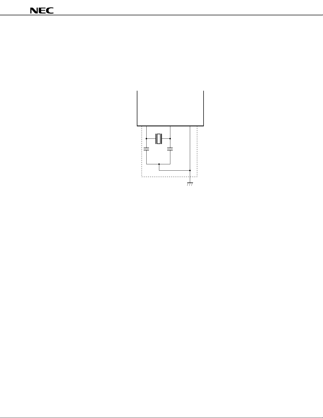
Compared with the main system clock oscillator, the watch clock oscillator, which is a low-gain circuit designed
to reduce current consumption, is more likely to cause noise-induced malfunctions. Therefore, special care should
be taken when using the watch clock oscillator.
The microcontroller can operate normally only when the oscillation is normal and stable. If a high-precision oscillator
frequency is required, consult with the oscillator manufacturer.
Figure 8-4. Notes on Connecting the Oscillator
PD784908
µ
X2
Cautions 1. Place the oscillator as close as possible to pins X1 and X2 (XT1 and XT2).
2. Do not let other signal lines cross that part of the circuit enclosed in broken lines.
X1 V
SS
Data Sheet U11680EJ2V0DS00
37
Page 38
µ
PD784907, 784908
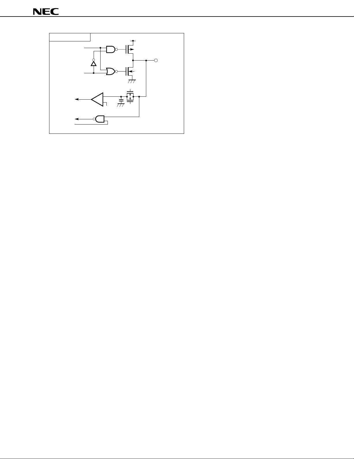
8.3 Real-Time Output Port
The real-time output port outputs data stored in the buffer, synchronized with a timer/counter 1 match interrupt or
external interrupt. Thus, pulse output that is free of jitter can be obtained.
Therefore, the real-time output port is best suited to applications (such as open-loop control over stepping motors)
where an arbitrary pattern is output at arbitrary intervals.
As shown in Figure 8-5, the real-time output port is built around port 0 and the port 0 buffer register (P0H, P0L).
Figure 8-5. Block Diagram of Real-Time Output Port
Internal bus
INTP0 (externally)
INTC10 (from timer/counter 1)
INTC11 (from timer/counter 1)
8
Real-time output port
control register
(RTPC)
Output trigger
control circuit
4
Port 0 buffer register
4
Output latch (P0)
P07
4
8
P0LP0H
4
P00
38
Data Sheet U11680EJ2V0DS00
Page 39
µ
PD784907, 784908
8.4 Timers/Counters
Three timer/counter units and one timer unit are incorporated.
Moreover, because seven interrupt requests are supported, these timers/counters can be used as seven timer/
counter units.
Table 8-2. Timers/Counters Operation
Name Timer/Counter 0 Timer/Counter 1 Timer/Counter 2 Timer 3
Item
Count width 8 bits —
16 bits
Operating mode Interval timer 2 ch 2 ch 2 ch 1 ch
External event counter —
One-shot timer — — —
Function Timer output 2 ch — 2 ch —
Toggle output — —
PWM/PPG output — —
One-shot pulse output
Real-time output — ——
Pulse width measurement 1 input 1 input 2 inputs —
Number of interrupt requests 2221
Note
———
Note The one-shot pulse output function makes the level of a pulse output active by software, and makes the level
of a pulse output inactive by hardware (interrupt request signal).
Note that this function differs from the one-shot timer function of timer/counter 2.
Data Sheet U11680EJ2V0DS00
39
Page 40
Timer/counter 0
Figure 8-6. Timer/Counter Block Diagram
Clear control
µ
PD784907, 784908
Software trigger
fXX/4
INTP3
Timer/counter 1
fXX/4
INTP0
Prescaler
Edge
detection
Prescaler
Event input
Edge
detection
INTP3
INTP0
Timer register 0
Selector
Compare register
Compare register
Capture register
Clear control
Timer register 1
(TM1/TM1W)
Selector
Compare register
(CR10/CR10W)
Capture/compare register
(CR11/CR11W)
Capture register
(CR12/CR12W)
(TM0)
(CR00)
(CR01)
(CR02)
Match
Match
Match
Match
OVF
TO0
TO1
Pulse output control
INTC00
INTC01
OVF
INTC10
To real-time
output port
INTC11
Timer/counter 2
fXX/4
INTP2/CI
INTP1
Edge
detection
Edge
detection
Timer 3
fXX/4
Remark OVF: Overflow flag
Prescaler
INTP2
Prescaler
Selector
INTP1
Clear control
Timer register 2
(TM2/TM2W)
Compare register
(CR20/CR20W)
Capture/compare register
(CR21/CR21W)
Capture register
(CR22/CR22W)
Timer register 3
(TM3/TM3W)
Compare register
(CR30/CR30W)
Match
Match
Clear
Match
OVF
TO2
TO3
Pulse output control
INTC20
INTC21
UART, CSI
INTC30
40
Data Sheet U11680EJ2V0DS00
Page 41

µ
PD784907, 784908
8.5 Watch Timer
As the count clock, either of two types of clock can be input to the watch timer: the main clock (6.29 MHz/12.58
MHz) or the watch clock (32.768 kHz). They can be selected using the control register. The watch clock is input to
the watch timer only. It is not input to the CPU or other peripheral circuits. Therefore, the speed of CPU operation
cannot be slowed by the watch clock.
Note
The watch timer generates interrupt signals (INTW), at 0.5-second intervals
, by dividing the count clock. At
the same time, the watch timer sets the interrupt request flag (WIF) (where WIF refers to bit 7 of the interrupt control
register (WIC)).
By switching modes, the INTW generation interval can be changed to about 1 ms (fast-forward mode: normal
operation speed × 512).
When the main clock is selected as the count clock, the watch timer stops if in STOP or IDLE standby mode, but
continues operating if in HALT standby mode. When the watch clock is selected as the count clock, the watch timer
continues operating regardless of the standby mode. The operation of the watch clock oscillator is controlled by means
of the watch timer mode register (WM).
µ
The watch timer of the
PD784908 does not have a buzzer output function.
Note After the operation is enabled, the time until first INTW generation is not 0.5 s.
Table 8-3. Relationship between Count Clock and Watch Timer Operation
Count Clock Selection Normal Operation Mode Standby Modes
HALT mode STOP mode IDLE mode
Main clock Operable Operable Stopped Stopped
Watch clock Operable Operable Operable Operable
The watch timer consists of a frequency divider which divides the count clock by 3 and a counter which divides
the frequency output from the frequency divider by 214. As the count clock, select the signal obtained by dividing the
internal system clock by 128 or that output by the watch clock oscillator.
Figure 8-7. Watch Timer Block Diagram
WM.3
Reset
Main clock
f
XX
/128
Division
by 3
Watch
clock
oscillator
ON/OFF
0
1
123456789 10111213 14
Counter Counter
0
SEL
SEL SEL
1
WM.2
1
INTW
0
WM.7
WM.6
Data Sheet U11680EJ2V0DS00
Main clock selection: 6.29 MHz
STBC.7
12.58 MHz
41
Page 42

µ
PD784907, 784908
8.6 PWM Output (PWM0, PWM1)
Two channels of PWM (pulse width modulation) output circuitry with a resolution of 12 bits and a repetition frequency
of 24.57 kHz (fCLK = 6.29 MHz) are incorporated. Low or high active level can be selected for the PWM output
channels, independently of each other. This output is best suited to DC motor speed control.
Figure 8-8. Block Diagram of PWM Output Unit
Internal bus
CLK
f
Prescaler
Remark n = 0, 1
(Modulo register)
15 0
PWMn
8-bit
down-counter
1/256
16
8 7 4 3
84
Pulse control
circuit
4-bit counter
8
PWM control register
(PWMC)
Reload
control
Output
control
PWMn (output pin)
42
Data Sheet U11680EJ2V0DS00
Page 43

µ
PD784907, 784908
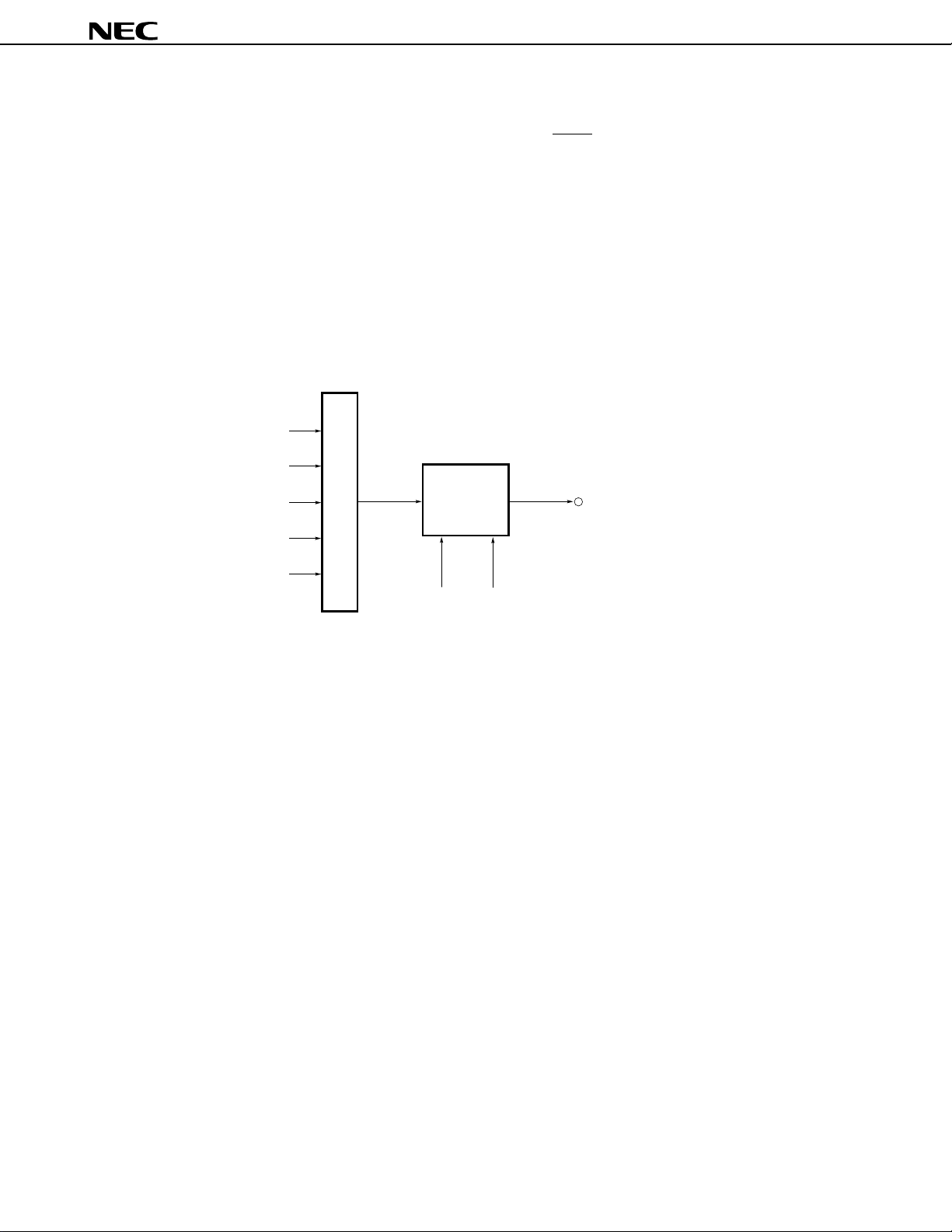
8.7 A/D Converter
An analog/digital (A/D) converter having 8 multiplexed analog inputs (ANI0 through ANI7) is incorporated.
The successive approximation system is used for conversion. The result of conversion is held in the 8-bit A/D
conversion result register (ADCR). Thus, speedy high-precision conversion can be achieved.
A/D conversion can be started in the following two ways:
• Hardware start: Conversion is started by trigger input (INTP5).
• Software start: Conversion is started by setting the bit of the A/D converter mode register (ADM).
After conversion has started, one of the following modes can be selected:
• Scan mode: Multiple analog inputs are selected sequentially to convert multiple pins.
• Select mode: A single analog input is selected at all times to enable conversion data to be obtained continuously.
ADM is used to specify the above modes, as well as the termination of conversion.
When the result of conversion is transferred to ADCR, an interrupt request (INTAD) is generated. Using this feature,
the results of conversion can be continuously transferred to memory by the macro service.
Cautions 1. For this product, apply the same voltage as the power supply voltage (AV
voltage input pin (AVREF1).
2. When port 7 is used as both an output port and A/D input line, do not manipulate the output
port while A/D conversion is in progress.
Figure 8-9. Block Diagram of A/D Converter
ANI0
ANI1
ANI2
ANI3
ANI4
ANI5
ANI6
ANI7
INTP5
Input selector
Edge
detection
circuit
A/D converter mode
register (ADM)
Sample and hold circuit
Conversion
trigger
Trigger enable
Voltage comparator
Successive
approximation
register (SAR)
Control
circuit
A/D conversion
result register (ADCR)
INTAD
8
Series resistor string
R/2
R
Tap selector
R/2
AV
DD
Connection
control
AV
REF1
AV
SS
DD) to the reference
A/D current cut selection
register (IEAD)
8
Internal bus
Data Sheet U11680EJ2V0DS00
8
43
Page 44

µ
PD784907, 784908
8.8 Serial Interface
Four independent serial interface channels are incorporated.
•
Asynchronous serial interface (UART)/3-wire serial I/O (IOE) × 2
•
Synchronous serial interface (CSI) × 2
• 3-wire serial I/O (IOE)
This makes it possible for communication with an external system and local communication within the system to
be simultaneously executed (see Figure 8-10).
Figure 8-10. Example of Serial Interface
UART + 3-wire serial I/O + 2-wire serial I/O
PD4711A
µ
RS-232-C
driver/receiver
Note Handshake line
PD784908 (master)
µ
[UART]
RxD
TxD
Port
SO1
SI1
SCK1
INTPm
Port
SI0
SO0
SCK0
INTPn
Port
[3-wire serial I/O]
Note
V
DD
Note
[2-wire serial I/O]
Slave
SI
SO
SCK
Port
INT
V
DD
Slave
SB0
SCK0
Port
INT
44
Data Sheet U11680EJ2V0DS00
Page 45

µ
PD784907, 784908
8.8.1 Asynchronous serial interface/3-wire serial I/O (UART/IOE)
Two serial interface channels, from which asynchronous serial interface mode and 3-wire serial I/O mode can be
selected, are provided.
(1) Asynchronous serial interface mode
In this mode, 1-byte data is transferred or received after a start bit.
A baud rate generator is incorporated to enable communication at a wide range of baud rates.
A baud rate can be defined by dividing the frequency of a clock signal input to the ASCK pin.
By using the baud rate generator, a baud rate conforming to the MIDI standard (31.25 kbps) can be obtained.
Figure 8-11. Block Diagram of Asynchronous Serial Interface Mode
Internal bus
RxD, RxD2
TxD, TxD2
Baud rate generator
XX
f
ASCK, ASCK2
Selector
1/2
n+1
Receive buffer
Receive
shift register
Reception
control parity
check
1/2m
1/2m
RXB, RXB2
INTSR,
INTSR2
INTSER,
INTSER2
Transmission
shift register
Transmission
control parity
bit addition
TXS, TXS2
INTST, INTST2
Remark f
XX: Oscillating frequency or external clock input frequency
n = 0 to 11
m = 16 to 30
Data Sheet U11680EJ2V0DS00
45
Page 46

µ
PD784907, 784908
(2) 3-wire serial I/O mode
In this mode, the master device makes the serial clock active to start transmission, then transfers 1-byte data
in synchronization with this clock.
This mode is designed for communication with a device incorporating a conventional synchronous serial interface.
Basically, three lines are used for communication: the serial clock line (SCK) and the two serial data lines (SI
and SO). In general, a handshake line is required to check the state of communication.
Figure 8-12. Block Diagram of 3-Wire Serial I/O Mode
Internal bus
Direction control
circuit
SIO1, SIO2
SI1, SI2
Shift register Output latch
SO1, SO2
SCK1, SCK2
Remark f
Serial clock counter
Serial clock
control circuit
XX: Oscillating frequency or external clock input frequency
n = 0 to 11
m = 1, 16 to 30
Interrupt
generator
Selector
1/m 1/2
INTCSI1,
INTCSI2
n+1
f
XX
46
Data Sheet U11680EJ2V0DS00
Page 47

µ
PD784907, 784908
8.8.2 Clocked serial interface (CSI)
With this interface, the master device makes the serial clock active to start transmission, then transfers 1-byte data
in synchronization with this clock.
Figure 8-13. Block Diagram of Clocked Serial Interface
Internal bus
SIn
SIOn register CSIMn register
Selector
SOn
SCKn
Remark f
Serial clock counter
XX: Oscillating frequency or external clock input frequency
n = 0, 3
Selector
INTCSIn
f
XX
/8
f
XX
/16
f
XX
/32
f
XX
/64
f
XX
/128
Data Sheet U11680EJ2V0DS00
47
Page 48
µ
PD784907, 784908
• 3-wire serial I/O mode
This mode is designed for communication with a device incorporating a conventional clocked serial interface.
Basically, three lines are used for communication: the serial clock line (SCKn) and serial data lines (SIn and SOn)
(n = 0, 3).
In general, a handshake line is required to check the state of communication.
8.9 Clock Output Function
The frequency of the CPU clock signal can be divided and output from the system. Moreover, the port can be used
as a 1-bit port.
The ASTB pin is also used as the CLKOUT pin, so that when this function is used, the local bus interface cannot
be used.
Figure 8-14. Block Diagram of Clock Output Function
f
CLK
f
CLK
/2
CLK
/4
f
Selector
CLK
/8
f
f
CLK
/16
Output control
Enable output Output level
CLKOUT
48
Data Sheet U11680EJ2V0DS00
Page 49
µ
PD784907, 784908
8.10 Edge Detection Function
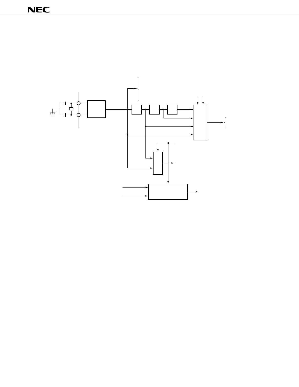
The interrupt input pins (NMI, INTP0 through INTP5) are used not only to input interrupt requests but also to input
trigger signals to the internal hardware units. Because these pins operate at the edge of the input signal, they have
an edge-detection function incorporated. Moreover, a noise elimination function is also provided to prevent erroneous
edge detection caused by noise.
Table 8-4. Noise Elimination Method of Interrupt Input Pins
Pin Name Detectable Edge Noise Elimination Method
NMI Rising edge or falling edge Analog delay
INTP0 to INTP3 Rising edge or falling edge, or both edges Clock sampling
Note
INTP4, INTP5 Analog delay
Note INTP0 is used for sampling clock selection.
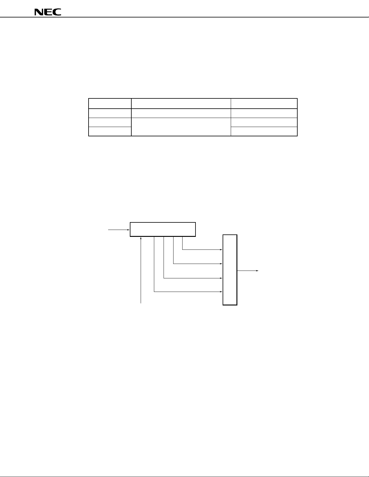
8.11 Watchdog Timer
A watchdog timer is incorporated to detect a CPU runaway. The watchdog timer, if not cleared by software within
a specified interval, generates a non-maskable interrupt request. Furthermore, once watchdog timer operation is
enabled, it cannot be disabled by software. The user can specify whether priority is placed on an interrupt request
based on the watchdog timer or on an interrupt request based on the NMI pin.
Figure 8-15. Block Diagram of Watchdog Timer
f
CLK
Clear signal
Timer
21
f
CLK
/2
20
CLK
/2
f
19
f
CLK
/2
17
f
CLK
/2
Selector
INTWDT
Data Sheet U11680EJ2V0DS00
49
Page 50
µ
PD784907, 784908
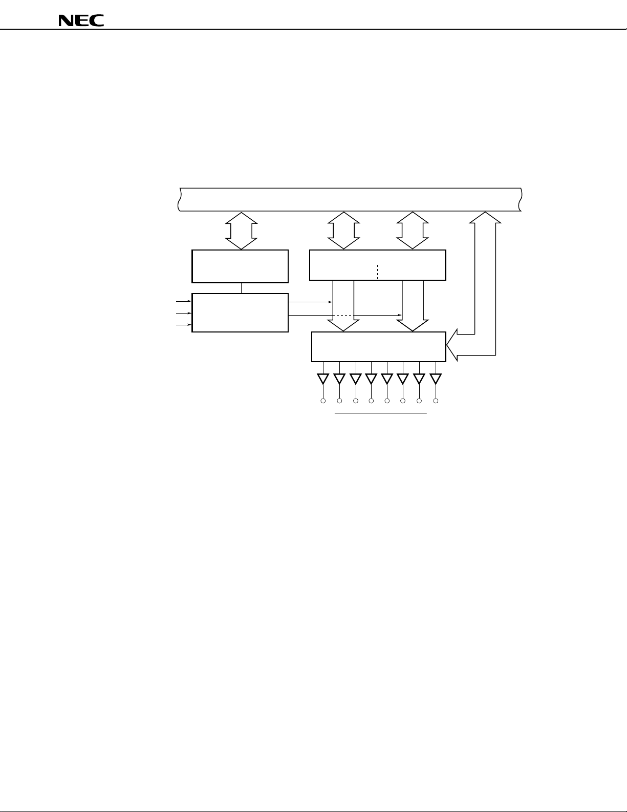
8.12 Simplified IEBus Controller
µ
A newly developed IEBus controller is incorporated into the
PD784908. This IEBus controller has fewer functions
than the IEBus interface function of previous product (incorporated into the 78K/0).
Table 8-5 compares the previous product and the new, simplified IEBus interface.
Table 8-5. Comparisons between Previous Product and Simplified IEBus Interface
Item Previous Product (IEBus Incorporated into 78K/0) Simplified IEBus
Communication mode Modes 0 to 2 Fixed to mode 1
Internal system clock 6.0 (6.29) MHz
Internal buffer size Transmission buffer 33 bytes (FIFO) Transmission/reception data register 1 byte
Reception buffer 40 bytes (FIFO)
Up to four frames can be received
CPU processing Processing before transmission start (data setting) Processing before transmission start (data setting)
Setting and control of each communication status Setting and control of each communication status
Data write to the transmission buffer Data write processing for every byte
Data read from the reception buffer Data read processing for every byte
Transmission control such as slave status
Control of multiple frames, remastering request
Hardware processing Bit processing Bit processing
(modulation/demodulation, error detection) (modulation/demodulation, error detection)
Field processing (generation, control) Field processing (generation, control)
Detection of arbitration results Detection of arbitration results
Parity processing (generation, error detection) Parity processing (generation, error detection)
ACK/NACK automatic response ACK/NACK automatic response
Automatic data retransmitting Automatic data retransmitting
Automatic remastering
Transmission such as automatic slave status
Reception of multiple frames
50
Data Sheet U11680EJ2V0DS00
Page 51
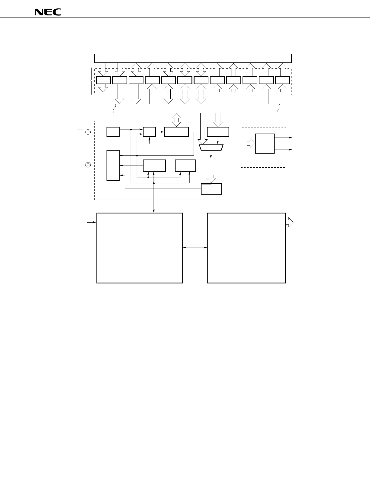
Figure 8-16. IEBus Controller
CPU interface section
µ
PD784907, 784908
Internal register section
RX
TX
CLK
88
12 12 12
BCR(8) DLR(8) USR(8) ISR(8) SSR(8) SCR(8) CCR(8)
UAR(12) SAR(12) PAR(12) CDR(8)
8
12 12 12
NF
MPX
IEBus interface section
MPX
TX/RX
Parity error
detector
PSR (8 bits)
8888888
DR(8)
888
Internal bus
8
Conflict
detector
12
8
12-bit latch
Comparator
ACK
generator
Interrupt
control
circuit
Interrupt control
section
88888
INT request
(vector, macro service)
5
Internal bus R/W
Bit processing section Field processing section
Data Sheet U11680EJ2V0DS00
51
Page 52

•
Hardware configuration and functions
The internal configuration of the IEBus consists mainly of the following six sections:
• CPU interface section
• Interrupt control section
• Internal register section
• Bit processing section
• Field processing section
• IEBus interface section
<CPU interface section>
Interfaces between the CPU (78K/IV) and the IEBus.
<Interrupt control section>
Passes interrupt request signals from the IEBus to the CPU.
<Internal register section>
Control register which stores the data in each field to control the IEBus.
µ
PD784907, 784908
<Bit processing section>
Generates and resolves the bit timing. Mainly consists of the bit sequence ROM, 8-bit preset timer, and
discriminator.
<Field processing section>
Generates each field in the communication frame. Mainly consists of the field sequence ROM, 4-bit down counter,
and discriminator.
<IEBus interface section>
Interface section of the external driver/receiver. Mainly consists of the noise filter, shift register, conflict detector,
parity detector, parity generator, and ACK/NACK generator.
52
Data Sheet U11680EJ2V0DS00
Page 53

µ
PD784907, 784908
9. INTERRUPT FUNCTION
The three types of interrupt request-response servicing, as shown in Table 9-1 below, can be selected by program.
Table 9-1. Servicing of Interrupt Request
Servicing Mode Servicing Agent Servicing PC and PSW Contents
Vectored interrupt Software Branches and executes a servicing routine Saves to and restores from the stack.
(servicing is arbitrary).
Context switching Automatically switches register banks, and Saves to or restores from fixed area in
branches and executes a servicing routine the register bank.
(servicing is arbitrary).
Macro service Firmware Executes data transfer between memory and Maintained
I/O (servicing is fixed).
9.1 Interrupt Source
Table 9-2 shows the interrupt sources available. As shown, interrupts are generated by 27 types of sources,
execution of the BRK and BRKCS instructions, or an operand error.
Four levels of interrupt servicing priority can be set. Priority levels can be set to nest control during interrupt servicing
or to simultaneously generate interrupt requests. However, nested macro services are performed without suspension.
When interrupt requests having the same priority level are generated, they are serviced according to the default
priority (fixed) (see Table 9-2).
Data Sheet U11680EJ2V0DS00
53
Page 54
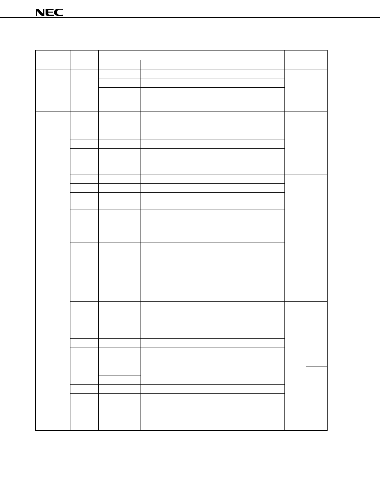
µ
PD784907, 784908
Table 9-2. Interrupt Source
Type Default Source Internal/ Macro
Priority
Software — BRK instruction Instruction execution — —
Non-maskable — NMI Detection of edge input on the pin External —
Maskable 0 (highest) INTP0 Detection of edge input on the pin (TM1/TM1W capture trigger) External √
1 INTP1 Detection of edge input on the pin (TM2/TM2W capture trigger)
2 INTP2 Detection of edge input on the pin (TM2/TM2W event counter
3 INTP3 Detection of edge input on the pin (TM0 capture trigger)
4 INTC00 TM0-CR00 match signal issued Internal √
5 INTC01 TM0-CR01 match signal issued
6 INTC10 TM1-CR10 match signal issued (in 8-bit operation mode)
7 INTC11 TM1-CR11 match signal issued (in 8-bit operation mode)
8 INTC20 TM2-CR20 match signal issued (in 8-bit operation mode)
9 INTC21 TM2-CR21 match signal issued (in 8-bit operation mode)
10 INTC30 TM3-CR30 match signal issued (in 8-bit operation mode)
11 INTP4 Detection of edge input on the pin External √
12 INTP5 Detection of edge input on the pin
13 INTAD A/D converter processing completed (ADCR transfer) Internal √
14 INTSER ASI0 reception error —
15 INTSR ASI0 reception completed or CSI1 transfer completed √
16 INTST ASI0 transmission completed
17 INTCSI CSI0 transfer completed
18 INTSER2 ASI2 reception error —
19 INTSR2 ASI2 reception completed or CSI2 transfer completed √
20 INTST2 ASI2 transmission completed
21 INTIE1 IEBus data access request
22 INTIE2 IEBus communication error and communication start/end
23 INTW Clock timer output
24 (lowest) INTCSI3 CSI3 transfer completed
Name Trigger
BRKCS instruction Instruction execution
Operand error When the MOV STBC,#byte, MOV WDM,#byte, or LOCATION
instruction is executed, exclusive OR of the byte operand and
byte does not produce FFH.
WDT Watchdog timer overflow Internal
input)
TM1W-CR10W match signal issued (in 16-bit operation mode)
TM1W-CR11W match signal issued (in 16-bit operation mode)
TM2W-CR20W match signal issued (in 16-bit operation mode)
TM2W-CR21W match signal issued (in 16-bit operation mode)
TM3W-CR30W match signal issued (in 16-bit operation mode)
(A/D converter start conversion trigger)
INTCSI1
INTCSI2
External Service
Remark ASI: Asynchronous serial interface
CSI: Clocked serial interface
54
Data Sheet U11680EJ2V0DS00
Page 55

µ
PD784907, 784908
9.2 Vectored Interrupt
When a branch to an interrupt servicing routine occurs, the vector table address corresponding to the interrupt
source is used as the branch address.
Interrupt servicing by the CPU consists of the following operations :
• When branching: Saves the CPU status (PC and PSW contents) to the stack.
• When returning: Restores the CPU status (PC and PSW contents) from the stack.
To return control from the servicing routine to the main routine, the RETI instruction is used.
The branch destination addresses must be within the range of 0 to FFFFH.
Table 9-3. Vector Table Address
Interrupt Source Vector Table Address
BRK instruction 003EH
Operand error 003CH
NMI 0002H
WDT 0004H
INTP0 0006H
INTP1 0008H
INTP2 000AH
INTP3 000CH
INTC00 000EH
INTC01 0010H
INTC10 0012H
INTC11 0014H
INTC20 0016H
INTC21 0018H
INTC30 001AH
INTP4 001CH
INTP5 001EH
INTAD 0020H
INTSER 0022H
INTSR 0024H
INTCSI1
INTST 0026H
INTCSI 0028H
INTSER2 002AH
INTSR2 002CH
INTCSI2
INTST2 002EH
Interrupt Source Vector Table Address
NTIE1 0032H
INTIE2 0034H
INTW 0036H
INTCSI3 0038H
Data Sheet U11680EJ2V0DS00
55
Page 56
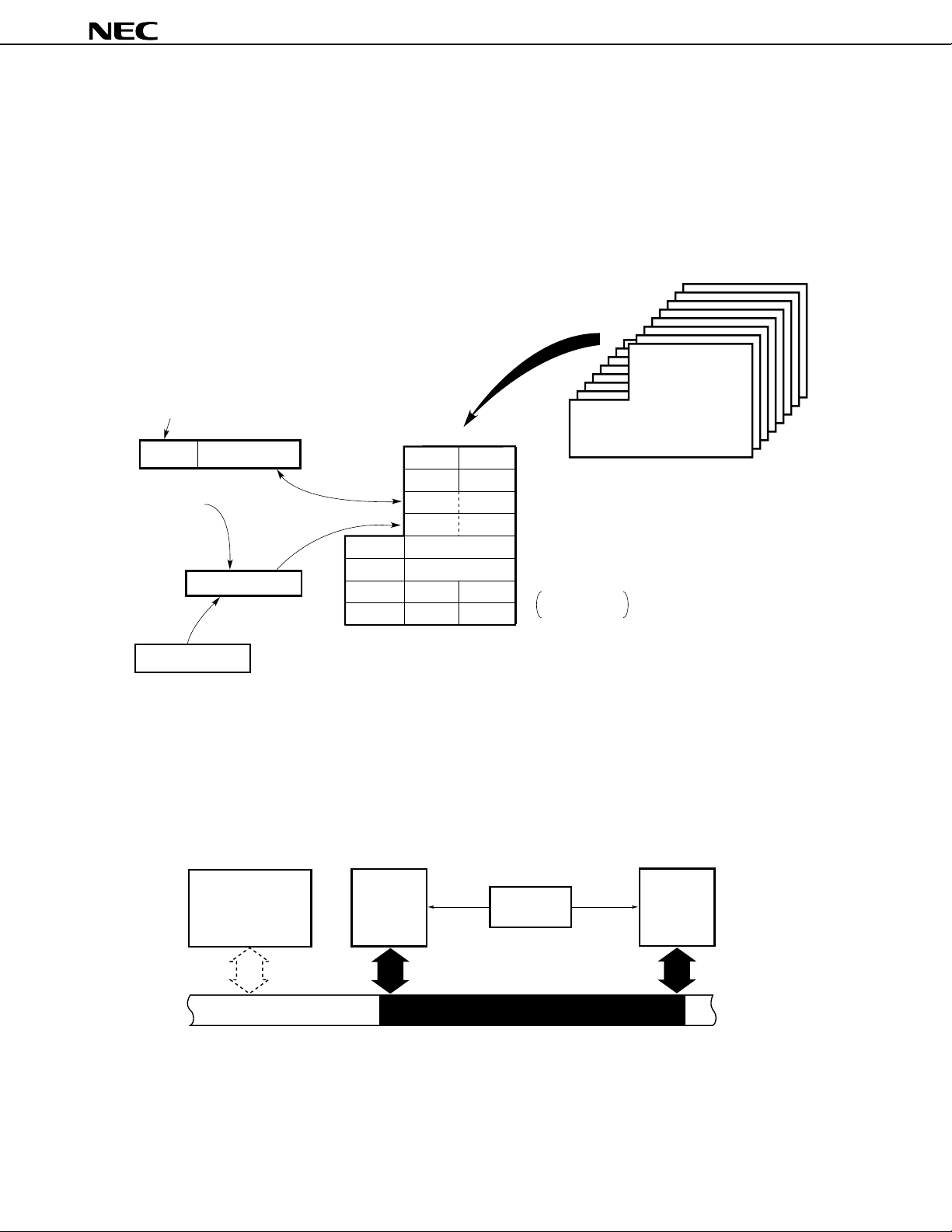
µ
PD784907, 784908
9.3 Context Switching
When an interrupt request is generated, or when the BRKCS instruction is executed, a predetermined register bank
is selected by the hardware. Then, a branch to a vector address stored in that register bank occurs. At the same
time, the contents of the current program counter (PC) and program status word (PSW) are stacked in the register
bank.
The branch address must be within the range of 0 to FFFFH.
Figure 9-1. Context Switching Operation When Interrupt Request Is Generated
0000B
<7>
PC19-16
<2>
Save
(Bits 8 to 11 of
temporary register)
Temporary register
<1>
Save
Transfer
PC15-0
<6>
Exchange
<5>
Save
Register bank n (n = 0-7)
AX
BC
R5 R4
R7
V
U
T
WL
DE
H
VP
UP
R6
Switching between register banks
<3>
(RBS0-RBS2 ← n)
<4>
RSS ← 0
IE ← 0
Register bank (0 to 7)
PSW
9.4 Macro Service
The macro service function enables data transfer between memory and special function registers (SFRs) without
requiring the intervention of the CPU. The macro service controller accesses both memory and SFRs within the same
transfer cycle to directly transfer data without having to perform data fetch.
Since the CPU status is neither saved nor restored, nor is data fetch performed, high-speed data transfer is possible.
Figure 9-2. Macro Service
CPU SFRMemory
Internal bus
Read
Write
Macro service
controller
Write
Read
56
Data Sheet U11680EJ2V0DS00
Page 57
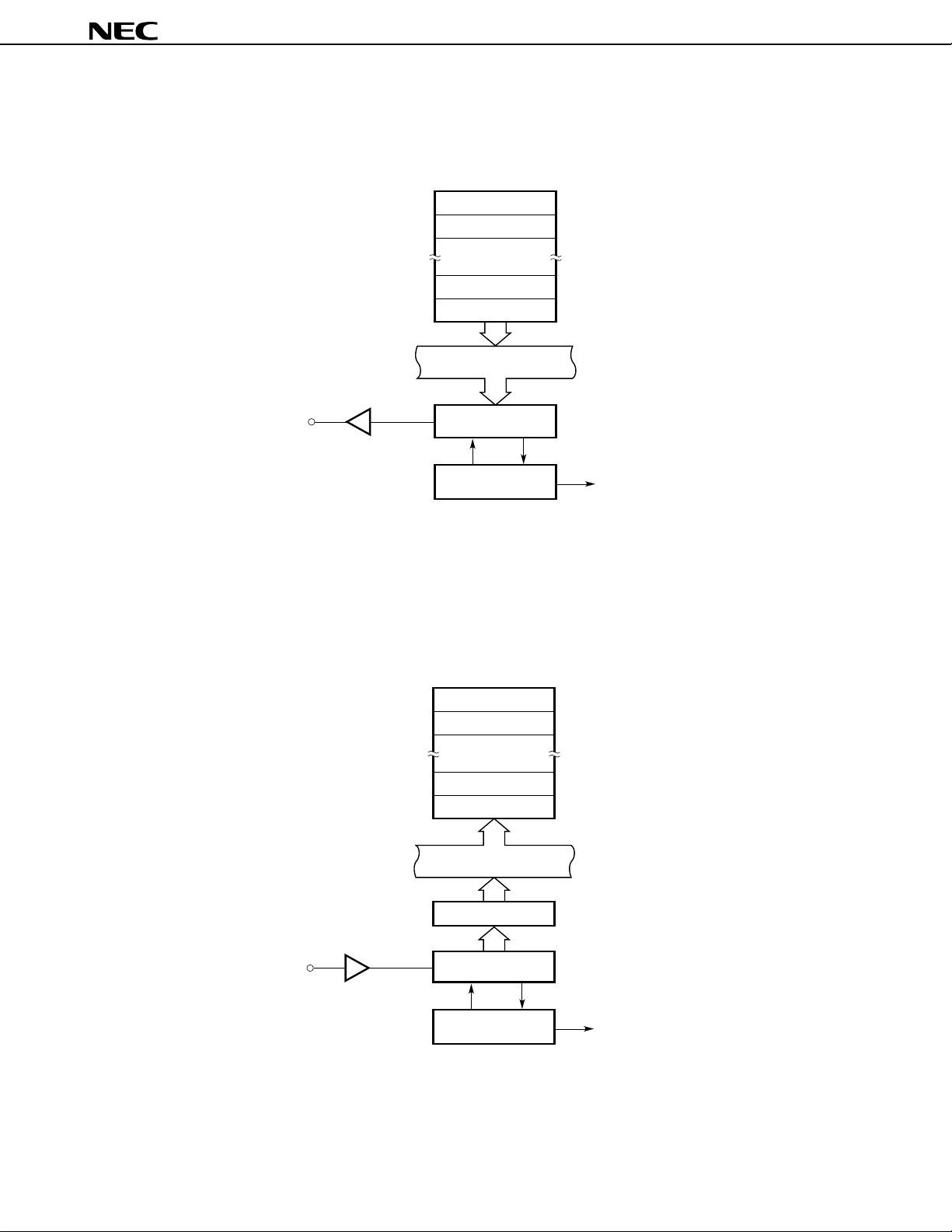
9.5 Examples of Macro Service Applications
(1) Serial interface transmission
Transmit data storage buffer (memory)
Data n
Data n - 1
Data 2
Data 1
Internal bus
µ
PD784907, 784908
TxD
Transmit
shift register
Transmit control
TXS (SFR)
INTST
Each time macro service request (INTST) is generated, the next transmit data is transferred from memory to TXS.
When data n (last byte) has been transferred to TXS (that is, once the transmit data storage buffer becomes
empty), vectored interrupt request (INTST) is generated.
(2) Serial interface reception
Receive data storage buffer (memory)
Data n
Data n - 1
Data 2
Data 1
Internal bus
RxD
Receive buffer
Receive
shift register
Receive control
RXB (SFR)
INTSR
Each time macro service request (INTSR) is generated, receive data is transferred from RXB to memory. When
data n (last byte) has been transferred to memory (that is, once the receive data storage buffer becomes full),
vectored interrupt request (INTSR) is generated.
Data Sheet U11680EJ2V0DS00
57
Page 58

µ
PD784907, 784908
(3) Real-time output port
INTC10 and INTC11 function as the output triggers for the real-time output ports. For these triggers, the macro
service can simultaneously set the next output pattern and interval. Therefore, INTC10 and INTC11 can be used
to independently control two stepping motors. They can also be applied to PWM and DC motor control.
Output pattern profile (memory) Output timing profile (memory)
P
n
P
n–1
P
2
P
1
T
n
T
n–1
T
2
T
1
P00 to P03
(SFR)
Internal bus
P0L
Output latch
Match
INTC10
Internal bus
CR10
TM1
(SFR)
Each time macro service request (INTC10) is generated, a pattern and timing data are transferred to the buffer
register (P0L) and compare register (CR10), respectively. When the contents of timer register 1 (TM1) and CR10
match, another INTC10 is generated, and the P0L contents are transferred to the output latch. When Tn (last
byte) is transferred to CR10, vectored interrupt request (INTC10) is generated.
For INTC11, the same operation as that performed for INTC10 is performed.
58
Data Sheet U11680EJ2V0DS00
Page 59

µ
PD784907, 784908
10. LOCAL BUS INTERFACE
The local bus interface enables the connection of external memory and I/O devices (memory mapped I/O) and
supports a 1-Mbyte memory space (see Figure 10-1).
Figure 10-1. Example of Local Bus Interface
PD784908
µ
A16 to A19
Decoder
RD
WR
REFRQ
Pseudo SRAM
PROM
PD27C1001A
µ
Kanji character
generator
PD24C1000
µ
AD0 to AD7
ASTB
A8 to A15
Latch
Data bus
Address bus
Gate array for I/O
expansion including
Centronics interface
circuit, etc.
10.1 Memory Expansion
By adding external memory, program memory or data memory can be expanded, 256 bytes at a time, to
approximately 1 Mbyte (seven steps).
Data Sheet U11680EJ2V0DS00
59
Page 60

µ
PD784907, 784908
10.2 Memory Space
The 1-Mbyte memory space is divided into eight spaces, each having a logical address. Each of these spaces
can be controlled using the programmable wait and pseudo-static RAM refresh functions.
Figure 10-2. Memory Space
FFFFFH
512 Kbytes
80000H
7FFFFH
256 Kbytes
40000H
3FFFFH
20000H
1FFFFH
10000H
0FFFFH
0C000H
0BFFFH
08000H
07FFFH
04000H
03FFFH
00000H
128 Kbytes
64 Kbytes
16 Kbytes
16 Kbytes
16 Kbytes
16 Kbytes
60
Data Sheet U11680EJ2V0DS00
Page 61

µ
PD784907, 784908
10.3 Programmable Wait
When the memory space is divided into eight spaces, a wait state can be separately inserted for each memory space
while the RD or WR signal is active. This prevents the overall system efficiency from being degraded even when
memory devices having different access times are connected.
In addition, an address wait function that extends the ASTB signal active period is provided to ensure the lapse
of the address decode time. (This function is set for the entire space.)
10.4 Pseudo-Static RAM Refresh Function
Refresh is performed as follows:
• Pulse refresh
A bus cycle is inserted where a refresh pulse is output on the REFRQ pin at regular intervals. When the memory
space is divided into eight, and a specified area is being accessed, refresh pulses can also be output on the
REFRQ pin as the memory is being accessed. This can prevent the refresh cycle from suspending normal
memory access.
• Power-down self-refresh
In standby mode, a low-level signal is output on the REFRQ pin to maintain the contents of pseudo-static RAM.
10.5 Bus Hold Function
A bus hold function is provided to facilitate connection to devices such as a DMA controller. When a bus hold request
signal (HLDRQ) is received from an external bus master, the address bus, address/data bus, and ASTB, RD, and
WR pins enter the high-impedance state, the bus hold acknowledge signal (HLDAK) is made active, and the bus is
released to the external bus master as soon as the current bus cycle is completed.
While the bus hold function is being used, the external wait and pseudo-static RAM refresh functions are disabled.
Data Sheet U11680EJ2V0DS00
61
Page 62

µ
PD784907, 784908
11. STANDBY FUNCTION
This function is to reduce the power consumption of the chip, and can be used in the following modes:
• HALT mode: Stops the operating clock of the CPU. This mode is used in combination with the normal operation
mode for intermittent operation to reduce the average power consumption.
• IDLE mode: Stops the entire system with the oscillator continuing operation. The power consumption in this
mode is close to that in the STOP mode. However, the time required to restore the normal program
operation from this mode is almost the same as that from the HALT mode.
• STOP mode: Stops the oscillator and thereby stops all the internal operations of the chip. Consequently, the
power consumption is minimized with only leakage current flowing.
These modes are programmable.
The macro service can be started from the HALT mode.
Figure 11-1. Standby Mode Status Transition
Macro service request
End of one operation
End of macro service
Interrupt request
RESET input
Set HALT
Note 2
Macro service request
End of one operation
HALT
(standby)
Macro
service
Notes 1, 3
INTW
NMI, INTP4, INTP5 input
STOP
(standby)
Wait for
oscillation
settling
Note 1
Set STOP
RESET input
Oscillation settling
time elapses
Set IDLE
INTW
IDLE
(standby)
Program
operation
Note 1
RESET input
Notes 1, 3
NMI, INTP4, INTP5 input
Request for masked interrupt
Notes 1. INTW, INTP4, and INTP5 are applied when not masked.
2. Only unmasked interrupt request
3. When the watch clock is operating
Remark NMI is valid only for an external input. The watchdog timer cannot be used for the release of standby
(STOP, HALT, or IDLE mode).
62
Data Sheet U11680EJ2V0DS00
Page 63

µ
PD784907, 784908
12. RESET FUNCTION
When a low-level signal is input to the RESET pin, the internal hardware becomes initialize status (reset status).
When the RESET input makes a low-to-high transition, the following data is loaded into the program counter (PC):
• Low-order 8 bits of the PC: Contents of address 0000H
• Intermediate 8 bits of the PC: Contents of address 0001H
• High-order 4 bits of the PC: 0
The PC contents are used as a branch destination address, and program execution starts from that address.
Therefore, a reset start can be performed from an arbitrary address.
The contents of each register can be set by software, as necessary.
The RESET input circuit incorporates a noise eliminator to prevent malfunctions caused by noise. This noise
eliminator is an analog delay sampling circuit.
Figure 12-1. Accepting Reset
Execute instruction
of reset start address
RESET
(input)
Internal reset signal
Delay
Delay
Start reset
Delay
End reset
Initialize PC
For power-on reset, the RESET signal must be held active until the oscillation stabilization time (approximately 40
ms) has elapsed.
Figure 12-2. Power-On Reset
Oscillation stabilization time Delay
V
DD
Initialize PC
Execute instruction of
reset start address
RESET
(input)
Internal reset signal
End reset
Data Sheet U11680EJ2V0DS00
63
Page 64
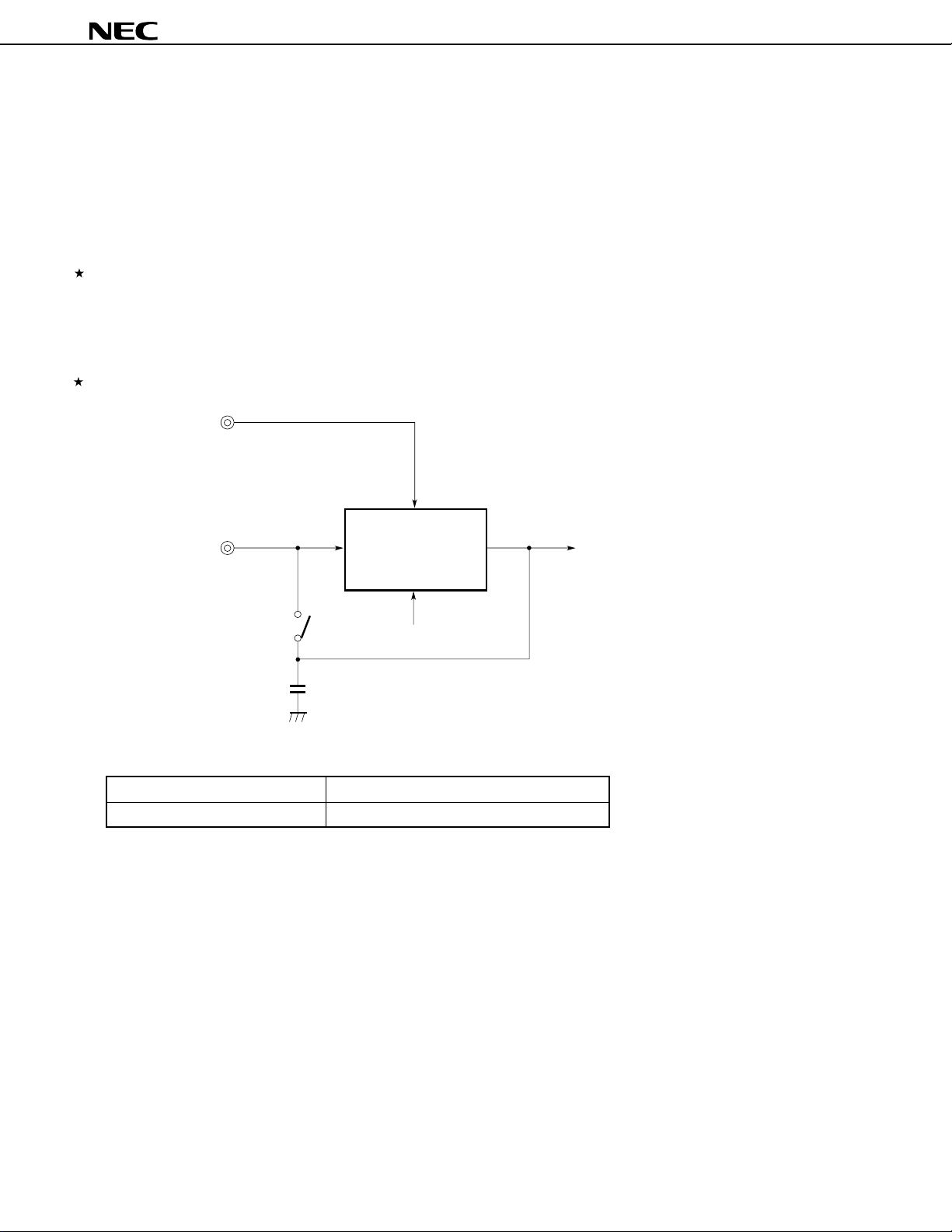
µ
PD784907, 784908
13. REGULATOR
The µPD784908 incorporates a regulator (a circuit which enables low-voltage operation) to reduce the current
consumption of the device. To enable or disable the operation of this regulator, specify the input level of the REGOFF
pin. To disable the operation of the regulator, input a high level signal to the REGOFF pin. To enable operation, input
a low level signal to the REGOFF pin.
When the regulator is turned on, the CPU enters low-power mode. It is recommended to operate this product using
this regulator.
µ
To stabilize the regulator output voltage, connect a capacitor (of about 1
connection pin).
When the regulator is stopped, apply the same level as V
DD to the REGC pin. Figure 13-1 is a block diagram of
the regulator's peripheral circuits.
Figure 13-1. Regulator Peripheral Circuits
REGOFF
Low level: Regulator is turned on.
High level: Regulator is turned off.
F) to the REGC pin (stabilizing capacitor
DD
V
REGC
1 F
µ
Regulator
Stops oscillation.
STBC.7
• Processing for the REGC pin
When the regulator is operating Connect a capacitor to stabilize the regulator.
When the regulator is stopped Supply the power supply voltage.
Internal power supply voltage
(Supplies to the CPU and
peripheral circuits.)
64
Data Sheet U11680EJ2V0DS00
Page 65
µ
PD784907, 784908
14. INSTRUCTION SET
(1) 8-bit instructions (The instructions in parentheses are combinations realized by describing A as r)
MOV, XCH, ADD, ADDC, SUB, SUBC, AND, OR, XOR, CMP, MULU, DIVUW, INC, DEC, ROR, ROL, RORC,
ROLC, SHR, SHL, ROR4, ROL4, DBNZ, PUSH, POP, MOVM, XCHM, CMPME, CMPMNE, CMPMNC, CMPMC,
MOVBK, XCHBK, CMPBKE, CMPBKNE, CMPBKNC, CMPBKC, CHKL, CHKLA
Table 14-1. Instruction List by 8-Bit Addressing
2nd operand #byte A r saddr sfr !addr16 mem r3 [WHL+] n None
r' saddr' !!addr24 [saddrp] PSWL [WHL–]
1st operand [%saddrg] PSWH
Note 6
A (MOV) (MOV) MOV
Note 1
ADD
r MOV (MOV) MOV MOV MOV MOV ROR
ADD
saddr MOV
ADD
sfr MOV MOV MOV PUSH
ADD
!addr16 MOV (MOV) MOV
!!addr24 ADD
mem MOV
[saddrp] ADD
[%saddrg]
mem3 ROR4
r3 MOV MOV
PSWL
PSWH
B, C DBNZ
STBC, WDM MOV
[TDE+] (MOV)
[TDE–]
(XCH) XCH
Note 1
(ADD)
Note 1
(XCH) XCH XCH XCH XCH DIVUW
(ADD)
(MOV)
Note 1
(ADD)
Note 1
(ADD)
(ADD)
MOVM
(ADD)
Note 1
ADD
Note 6
MOV MOV INC
Note 1
ADD
Note 1
ADD
Note 1
Note 1
Note 1
Note 4
(MOV)
(XCH)
Note
1
(ADD)
Note 1
ADD
Note 1
XCH DEC
ADD
Note 1
MOV (MOV) MOV MOV (MOV)
Note 6
(XCH) (XCH) XCH (XCH)
Notes 1, 6
Note 1
Note 1
(ADD)
ADD
Note 1
Note 1
ADD
Note 1
ADD
Note 1
(ADD)
MOVBK
Note 1
Note 5
Note 3
MULU
INC
DEC
DBNZ
POP
CHKL
CHKLA
ROL4
Note 2
Notes 1. ADDC, SUB, SUBC, AND, OR, XOR, and CMP are the same as ADD.
2. There is no second operand, or the second operand is not an operand address.
3. ROL, RORC, ROLC, SHR, and SHL are the same as ROR.
4. XCHM, CMPME, CMPMNE, CMPMNC, and CMPMC are the same as MOVM.
5. XCHBK, CMPBKE, CMPBKNE, CMPBKNC, and CMPBKC are the same as MOVBK.
6. When saddr is saddr2 with this combination, an instruction with a short code exists.
Data Sheet U11680EJ2V0DS00
65
Page 66

µ
PD784907, 784908
(2) 16-bit instructions (The instructions in parentheses are combinations realized by describing AX as rp)
MOVW, XCHW, ADDW, SUBW, CMPW, MULUW, MULW, DIVUX, INCW, DECW, SHRW, SHLW, PUSH, POP,
ADDWG, SUBWG, PUSHU, POPU, MOVTBLW, MACW, MACSW, SACW
Table 14-2. Instruction List by 16-Bit Addressing
2nd operand #word AX rp saddrp sfrp !addr16 mem [WHL+] byte n None
rp' saddrp' !!addr24 [saddrp]
1st operand [%saddrg]
AX (MOVW) (MOVW) (MOVW)
Note 1
ADDW
rp MOVW (MOVW) MOVW MOVW MOVW MOVW SHRW
ADDW
saddrp MOVW
ADDW
sfrp MOVW MOVW MOVW PUSH
ADDW
!addr16 MOVW (MOVW) MOVW
!!addr24
mem MOVW
[saddrp]
[%saddrg]
PSW PUSH
SP ADDWG
SUBWG
post PUSH
[TDE+] (MOVW) SACW
byte MACW
(XCHW) (XCHW)
Note 1
(ADD)
Note 1
(XCHW) XCHW XCHW XCHW SHLW INCW
Note 1
(ADDW)
Note 3
(MOVW)
Note 1
Note 1
(ADDW)
(ADDW)
Note 1
Note 1
Note 1
(ADDW)
Note 1
ADDW
MOVW MOVW INCW
Note 1
ADDW
Note 1
ADDW
Note 3
(MOVW)
(XCHW)
(ADDW)
ADDW
XCHW DECW
ADDW
MOVW (MOVW) MOVW (MOVW)
Note 3
(XCHW) XCHW XCHW (XCHW)
Notes 1,3
Note 1
Note 1
(ADDW)
Note 1
ADDW
Note 1
MULW
DECW
POP
MOVTBLW
POP
POP
PUSHU
POPU
MACSW
Note 2
Note 4
Notes 1. SUBW and CMPW are the same as ADDW.
2. There is no second operand, or the second operand is not an operand address.
3. When saddrp is saddrp2 with this combination, an instruction with a short code exists.
4. MULUW and DIVUX are the same as MULW.
66
Data Sheet U11680EJ2V0DS00
Page 67
µ
PD784907, 784908
(3) 24-bit instructions (The instructions in parentheses are combinations realized by describing WHL as rg)
MOVG, ADDG, SUBG, INCG, DECG, PUSH, POP
Table 14-3. Instruction List by 24-Bit Addressing
2nd operand #imm24 WHL rg saddrg !!addr24 mem1 [%saddrg] SP None
1st operand rg'
WHL (MOVG) (MOVG) (MOVG) (MOVG) (MOVG) MOVG MOVG MOVG
(ADDG) (ADDG) (ADDG) ADDG
(SUBG) (SUBG) (SUBG) SUBG
rg MOVG (MOVG) MOVG MOVG MOVG INCG
ADDG (ADDG) ADDG DECG
SUBG (SUBG) SUBG PUSH
saddrg (MOVG) MOVG
!!addr24 (MOVG) MOVG
mem1 MOVG
[%saddrg] MOVG
SP MOVG MOVG INCG
Note There is no second operand, or the second operand is not an operand address.
Note
POP
DECG
Data Sheet U11680EJ2V0DS00
67
Page 68
(4) Bit manipulation instructions
MOV1, AND1, OR1, XOR1, SET1, CLR1, NOT1, BT, BF, BTCLR, BFSET
Table 14-4. Bit Manipulation Instruction List by Addressing
µ
PD784907, 784908
2nd operand CY saddr.bit sfr.bit /saddr.bit /sfr.bit None
A.bit X.bit /A.bit /X.bit
PSWL.bit PSWH.bit /PSWL.bit /PSWH.bit
mem2.bit /mem2.bit
1st operand !addr16.bit !!addr24.bit /!addr16.bit /!!addr24.bit
CY MOV1 AND1 NOT1
AND1 OR1 SET1
OR1 CLR1
XOR1
saddr.bit MOV1 NOT1
sfr.bit SET1
A.bit CLR1
X.bit BF
PSWL.bit BT
PSWH.bit BTCLR
mem2.bit BFSET
!addr16.bit
!!addr24.bit
Note There is no second operand, or the second operand is not an operand address.
Note
68
Data Sheet U11680EJ2V0DS00
Page 69
µ
PD784907, 784908
(5) Call/return instructions and branch instructions
CALL, CALLF, CALLT, BRK, RET, RETI, RETB, RETCS, RETCSB, BRKCS, BR, BNZ, BNE, BZ, BE, BNC, BNL,
BC, BL, BNV, BPO, BV, BPE, BP, BN, BLT, BGE, BLE, BGT, BNH, BH, BF, BT, BTCLR, BFSET, DBNZ
Table 14-5. Instruction List by Call/Return and Branch Instruction Addressing
Instruction $addr20 $!addr20 !addr16 !!addr20 rp rg [rp] [rg] !addr11 [addr5] RBn None
address
operand
Note
Basic BC
instruction BR BR BR BR BR BR BR BR RET
Compound BF
instruction BT
BTCLR
BFSET
DBNZ
CALL CALL CALL CALL CALL CALL CALL CALLF CALLF BRKCS BRK
RETCS RETI
RETCSB RETB
Note BNZ, BNE, BZ, BE, BNC, BNL, BL, BNV, BPO, BV, BPE, BP, BN, BLT, BGE, BLE, BGT, BNH, and BH are
the same as BC.
(6) Other instructions
ADJBA, ADJBS, CVTBW, LOCATION, SEL, NOT EI, DI, SWRS
Data Sheet U11680EJ2V0DS00
69
Page 70
µ
PD784907, 784908
15. ELECTRICAL SPECIFICATIONS
Absolute Maximum Ratings (TA = 25°C)
Parameter Symbol Conditions Ratings Unit
Supply voltage VDD –0.3 to +6.5 V
AVDD –0.3 to VDD + 0.3 V
AVSS –0.3 to +0.3 V
Input voltage VI1 –0.3 to VDD + 0.3 V
Analog input voltage VAN AVSS – 0.3 to AVREF1 + 0.3 V
Output voltage VO –0.3 to VDD + 0.3 V
Output current, low IOL Per pin 10 mA
Total of P00 to P07, P30 to 50 mA
P37, P54 to P57, P60 to P67,
and P100 to P107 pins
Total of P10 to P17, P40 to 50 mA
P47, P50 to P53, P70 to P77,
P90 to P97, PWM0, PWM1,
and TX pins
Output current, high IOH Per pin –6 mA
Total of P00 to P07, P30 to –30 mA
P37, P54 to P57, P60 to P67,
and P100 to P107 pins
Total of P10 to P17, P40 to –30 mA
P47, P50 to P53, P70 to P77,
P90 to P97, PWM0, PWM1,
and TX pins
A/D converter reference input AVREF1 –0.3 to VDD + 0.3 V
voltage
Operating ambient temperature TA –40 to +85 °C
Storage temperature Tstg –65 to +150 °C
Caution Product quality may suffer if the absolute maximum rating is exceeded even momentarily for
any parameter. That is, the absolute maximum ratings are rated values at which the product
is on the verge of suffering physical damage, and therefore the product must be used under
conditions that ensure that the absolute maximum ratings are not exceeded.
Remark Unless otherwise specified, the characteristics of a alternate-function pin are the same as those of a port
pin.
70
Data Sheet U11680EJ2V0DS00
Page 71
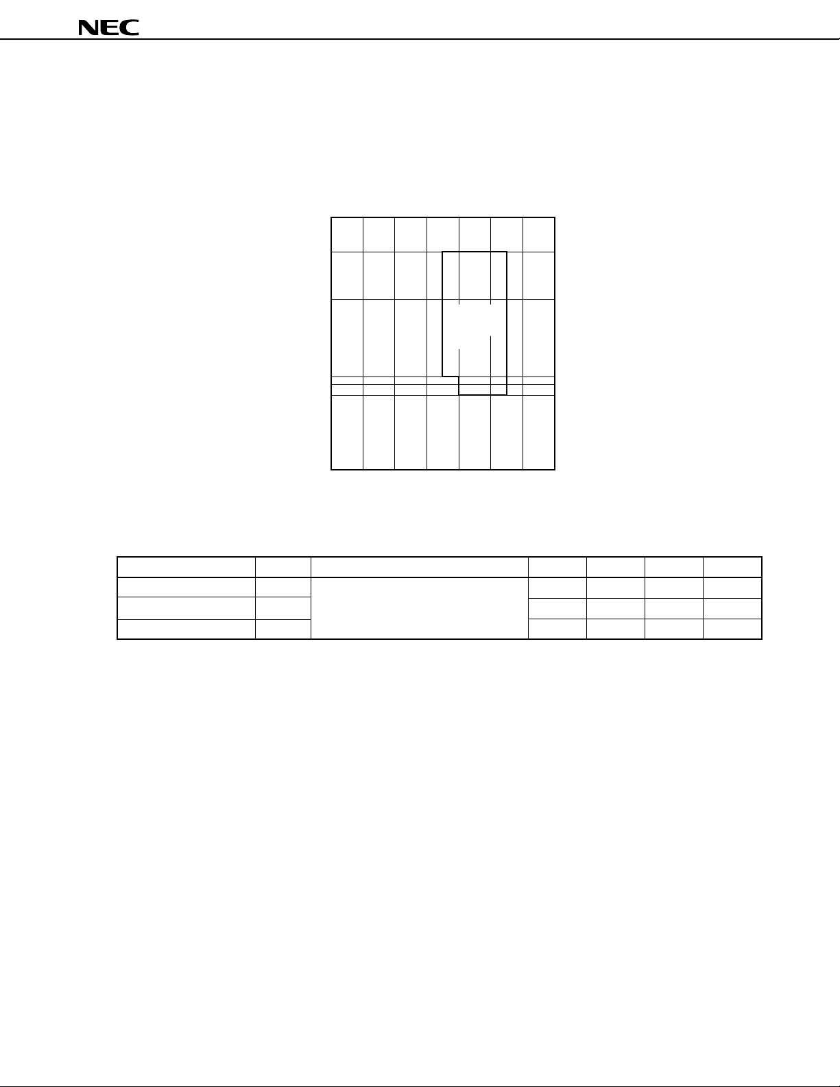
Operating Conditions
• Operating ambient temperature (T
A): –40°C to +85°C
• Power supply voltage and clock cycle time: see Figure 15-1 .
• Selection of internal regulator (REGOFF pin: low-level input)
Figure 15-1. Power Supply Voltage and Clock Cycle Time
10,000
4,000
µ
PD784907, 784908
1,000
159
100
79
Clock cycle time tCYK [ns]
10
01234567
Power supply voltage [V]
Guaranteed
operating
range
Capacitance (TA = 25°C, VDD = VSS = 0 V)
Parameter Symbol Conditions MIN. TYP. MAX. Unit
Input capacitance CI f = 1 MHz 15 pF
Output capacitance CO
I/O capacitance CIO 15 pF
Unmeasured pins returned to 0 V.
15 pF
Data Sheet U11680EJ2V0DS00
71
Page 72
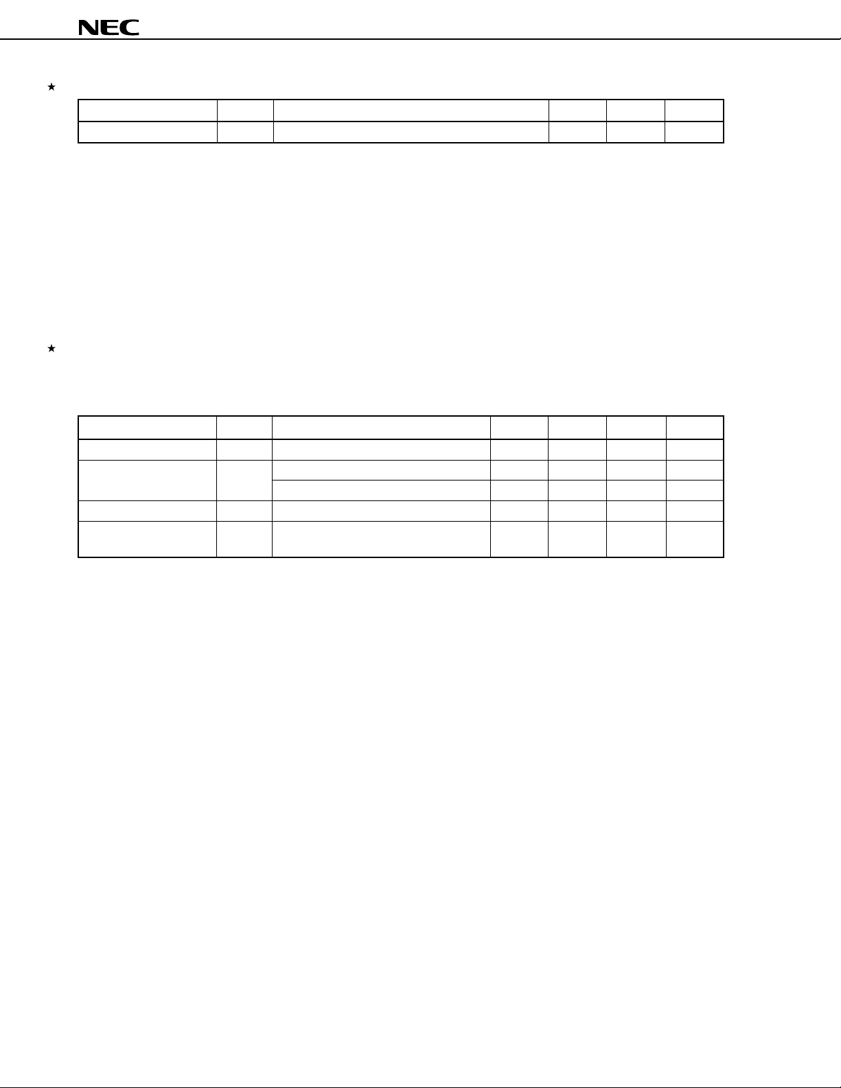
µ
PD784907, 784908
Main Oscillator Characteristics (TA = –40 to +85°C, VDD = 3.5 to 5.5 V, VSS = 0 V)
Parameter Symbol Conditions MIN. MAX. Unit
Oscillator frequency fXX Ceramic resonator or crystal resonator 2 12.58 MHz
Caution When using the clock generator, wire to avoid adverse influence from wiring capacitance.
• Keep the wiring length as short as possible.
• Do not cross the wiring with other signal lines.
• Do not route the wiring near a signal line through which a high fluctuating current flows.
• Make the ground point of the oscillator capacitor the same potential as V
SS1. Do not ground
the capacitor to a ground pattern in which a high current flows.
• Do not fetch signals from the oscillator.
Remark Connect a 12.582912 MHz or 6.291456 MHz oscillator to operate the internal clock timer with the main
clock.
Clock Oscillator Characteristics (T
Parameter Symbol Conditions MIN. TYP. MAX. Unit
Oscillator frequency fXT Ceramic resonator or crystal resonator 32 32.768 35 kHz
Oscillation stabilization tSXT VDD = 4.5 to 5.5 V 1.2 2 s
time
Oscillation hold voltage VDDXT 3.5 5.5 V
Watch timer operating V
voltage
DDW 3.5 5.5 V
A = –40 to +85°C, VDD = 3.5 to 5.5 V, VSS = 0 V)
10 s
72
Data Sheet U11680EJ2V0DS00
Page 73
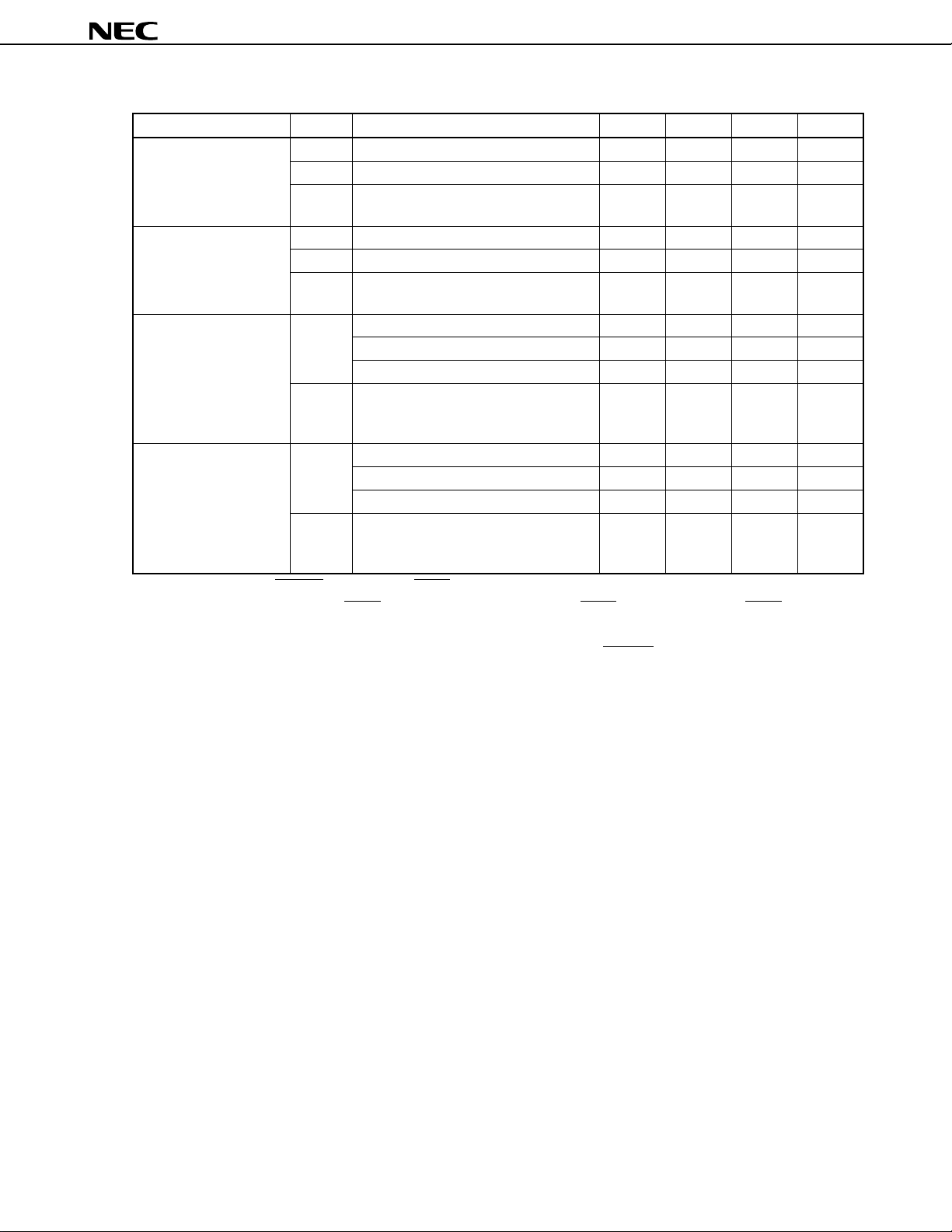
µ
PD784907, 784908
DC Characteristics (TA = –40 to +85°C, VDD = AVDD = 3.5 to 5.5 V, VSS = AVSS = 0 V) (1/2)
Parameter Symbol Conditions MIN. TYP. MAX. Unit
Input voltage, low
Input voltage, high VIH1 For pins other than Notes 1 and 2 0.7VDD VDD + 0.3 V
Output voltage, low VOL1 IOL = 20 µA 0.1 V
Output voltage, high VOH1 IOH = –20 µAVDD – 0.1 V
Note 5
VIL1 For pins other than Notes 1 and 2 –0.3 0.3VDD V
VIL2 For pins described in Note 1 –0.3 0.2VDD V
VIL3 VDD = 4.5 to 5.5 V –0.3 +0.8 V
For pins described in Note 2
VIH2 For pins described in Note 1 0.8VDD VDD + 0.3 V
VIH3 VDD = 4.5 to 5.5 V 2.2 V DD + 0.3 V
For pins described in Note 2
IOL = 100 µA 0.2 V
IOL = 2 mA 0.4 V
VOL2 IOL = 8 mA 1.0 V
For pins described in Note 4
VDD = 4.5 to 5.5 V
IOH = –100 µAVDD – 0.2 V
IOH = –2 mA VDD – 0.4 V
VOH2 V DD = 4.5 to 5.5 V VDD – 1.0 V
IOH = –5 mA
For pins described in Note 3
Notes 1. X1, X2, RESET, P12/ASCK2/SCK2, P20/NMI, P21/INTP0, P22/INTP1, P23/INTP2/CI, P24/INTP3,
P25/INTP4/ASCK/SCK1, P26/INTP5, P27/SI0, P32/SCK0, P33/SO0, P105/SCK3, P106/SI3,
P107/SO3, XT1, XT2
2. P40/AD0 to P47/AD7, P50/A8 to P57/A15, P60/A16 to P67/REFRQ/HLDAK, P00 to P07
3. P00 to P07
4. P10 to P17, P40/AD0 to P47/AD7, P50/A8 to P57/A15
5. Other than pull-up resistors
Data Sheet U11680EJ2V0DS00
73
Page 74

µ
PD784907, 784908
DC Characteristics (TA = –40 to +85°C, VDD = AVDD = 3.5 to 5.5 V, VSS = AVSS = 0 V) (2/2)
Parameter Symbol Conditions MIN. TYP. MAX. Unit
Input leakage current ILI1 0 V ≤ VI ≤ VDD For pins other than ±10
X1 and XT1
ILI2 X1 and XT1 ±20
Output leakage current I LO 0 V ≤ VO ≤ VDD ±10
VDD supply current
Pull-up resistor RL VI = 0 V X1 and XT1 15 80 kΩ
Note
IDD1 Operation mode fXX = 12.58 MHz 10 20 mA
VDD = 4.0 to 5.5 V
fXX = 6.29 MHz 5 10 mA
VDD = 3.5 to 5.5 V
IDD2 HALT mode fXX = 12.58 MHz 2.0 4.0 mA
VDD = 4.0 to 5.5 V
fCLK = fXX/8
(STBC = B1H)
Peripheral operation
stops.
f
XX = 6.29 MHz 1.2 2.4 mA
VDD = 3.5 to 5.5 V
fCLK = fXX/8
(STBC = 31H)
Peripheral operation
stops.
IDD3 IDLE mode fXX = 12.58 MHz 0.6 1.2 mA
VDD = 4.0 to 5.5 V
fXX = 6.29 MHz 0.3 0.6 mA
VDD = 3.5 to 5.5 V
µ
A
µ
A
µ
A
Note These values are valid when the internal regulator is ON (REGOFF pin = L level). They do not include the
DD and AVREF1 currents.
AV
74
Data Sheet U11680EJ2V0DS00
Page 75

µ
PD784907, 784908
AC Characteristics (TA = –40 to +85°C, VDD = AVDD = 3.5 to 5.5 V, AVSS = VSS = 0 V)
(1) Read/write operation
Parameter Symbol Conditions MIN. MAX. Unit
Address setup time (to ASTB↓)tSAST VDD = 5.0 V (0.5 + a)T – 11 29 ns
ASTB high-level width tWSTH VDD = 5.0 V (0.5 + a)T – 17 23 ns
Address hold time (from ASTB↓)tHSTLA VDD = 5.0 V 0.5T – 19 21 ns
Address hold time (from RD↑)tHRA VDD = 5.0 V 0.5T – 14 26 ns
Delay from address to RD↓ t DAR VDD = 5.0 V (1 + a)T – 5 74 ns
Address float time (from RD↓)tFRA 0ns
Data input time from address tDAID VDD = 5.0 V (2.5 + a + n)T – 37 400 ns
Data input time from
Data input time from RD↓ tDRID VDD = 5.0 V (1.5 + n)T – 40 238 ns
Delay from ASTB↓ to RD↓ tDSTR VDD = 5.0 V 0.5T – 9 31 ns
Data hold time (from RD↑)tHRID 0ns
Address active time from RD↑ tDRA VDD = 5.0 V 0.5T – 2 38 ns
Delay from RD↑ to ASTB↑ tDRST VDD = 5.0 V 0.5T – 9 31 ns
RD low-level width tWRL VDD = 5.0 V (1.5 + n)T – 25 94 ns
Delay from address↓ to WR↓ tDAW VDD = 5.0 V (1 + a)T – 5 74 ns
Address hold time (from WR↑)tHWA VDD = 5.0 V 0.5T – 14 26 ns
Delay from ASTB↓ to data output tDSTOD VDD = 5.0 V 0.5T + 15 55 ns
Delay from WR↓ to data output tDWOD 15 ns
Delay from ASTB↓ to WR↓ t DSTW VDD = 5.0 V 0.5T – 9 31 ns
Data setup time (to WR↑)tSODWR VDD = 5.0 V (1.5 + n)T – 20 99 ns
Data hold time (from WR↑)tHWOD VDD = 5.0 V 0.5T – 14 26 ns
Delay from WR↑ to ASTB↑ tDWST VDD = 5.0 V 0.5T – 9 31 ns
WR low-level width tWWL VDD = 5.0 V (1.5 + n)T – 25 94 ns
ASTB↓
tDSTID VDD = 5.0 V (2 + n)T – 35 283 ns
Remark T: tCYK (system clock cycle time) VDD = 5.0 V T = 79 ns (MIN.)
a: 1 during address wait, otherwise, 0
n: number of wait states (n ≥ 0)
Data Sheet U11680EJ2V0DS00
75
Page 76

µ
PD784907, 784908
(2) External wait timing
Parameter Symbol Conditions MIN. MAX. Unit
WAIT↓ input time from address tDAWT VDD = 5.0 V (2 + a)T – 40 198 ns
WAIT↓ input time from ASTB↓ tDSTWT VDD = 5.0 V 1.5T – 40 79 ns
WAIT hold time from ASTB↓ t HSTWT VDD = 5.0 V (0.5 + n)T + 5 124 ns
Delay from ASTB↓ to WAIT↑ t DSTWTH VDD = 5.0 V (1.5 + n)T – 40 238 ns
WAIT↓ input time from RD↓ tDRWTL VDD = 5.0 V T – 40 39 ns
WAIT hold time from RD↓ t HRWT VDD = 5.0 V nT + 5 84 ns
Delay from RD↓ to WAIT↑ tDRWTH VDD = 5.0 V (1 + n)T – 40 198 ns
Data input time from WAIT↑ tDWTID VDD = 5.0 V 0.5T – 5 35 ns
Delay from WAIT↑ to RD↑ tDWTR VDD = 5.0 V 0.5T 40 ns
Delay from WAIT↑ to WR↑ tDWTW VDD = 5.0 V 0.5T 40 ns
WAIT↓ input time from WR↓ tDWWTL VDD = 5.0 V T – 40 39 ns
WAIT hold time from WR↓ tHWWT VDD = 5.0 V nT + 5 84 ns
Delay from WR↓ to WAIT↑ tDWWTH VDD = 5.0 V (1 + n)T – 40 198 ns
Remark T: tCYK (system clock cycle time) VDD = 5.0 V T = 79 ns (MIN.)
a: 1 during address wait, otherwise, 0
n: number of wait states (n ≥ 0)
76
Data Sheet U11680EJ2V0DS00
Page 77

µ
PD784907, 784908
(3) Bus hold timing
Parameter Symbol Conditions MIN. MAX. Unit
Delay from HLDRQ↑ to float tFQHC VDD = 5.0 V (2 + 4 + a + n)T + 50 765 ns
Delay from HLDRQ↑ to HLDAK↑ t DHQHHAH VDD = 5.0 V (3 + 4 + a + n)T + 30 825 ns
Delay from float to HLDAK↑ tDCFHA VDD = 5.0 V T + 30 109 ns
Delay from HLDRQ↓ to HLDAK↓ t DHQLHAL VDD = 5.0 V 2T + 40 199 ns
Delay from HLDRQ↓ to active tDHAC VDD = 5.0 V T – 20 59 ns
Remark T: tCYK (system clock cycle time) VDD = 5.0 V T = 79 ns (MIN.)
a: 1 during address wait, otherwise, 0
n: number of wait states (n ≥ 0)
(4) Refresh timing
Parameter Symbol Conditions MIN. MAX. Unit
Random read/write cycle time tRC VDD = 5.0 V 3T 238 ns
REFRQ low-level pulse width tWRFQL VDD = 5.0 V 1.5T – 25 94 ns
Delay from ASTB↓ to REFRQ tDSTRFQ VDD = 5.0 V 0.5T – 9 31 ns
Delay from RD↑ to REFRQ tDRRFQ V DD = 5.0 V 1.5T – 9 110 ns
Delay from WR↑ to REFRQ tDWRFQ VDD = 5.0 V 1.5T – 9 110 ns
Delay from REFRQ↑ to ASTB tDRFQST VDD = 5.0 V 0.5T – 9 31 ns
REFRQ high-level pulse width tWRFQH VDD = 5.0 V 1.5T – 25 94 ns
Remark T: tCYK (system clock cycle time) VDD = 5.0 V T = 79 ns (MIN.)
Data Sheet U11680EJ2V0DS00 77
Page 78

µ
PD784907, 784908
Serial Operation (TA = –40 to +85°C, VDD = 3.5 to 5.5 V, AVSS = VSS = 0 V)
(1) CSI, CSI3
Parameter Symbol Conditions MIN. MAX. Unit
Serial clock cycle time tCYSK0 Input f CLK = fXX 8/fXX ns
(SCK0, SCK3)
Serial clock low-level width tWSKL0 Input fCLK = fXX 4/fXX – 40 ns
(SCK0, SCK3)
Serial clock high-level width tWSKH0 Input fCLK = fXX 4/fXX – 40 ns
(SCK0, SCK3)
SI0, SI3 setup time t
(to SCK0, SCK3↑)
SI0, SI3 hold time tHSSK0 External clock 1/fCLK + 80 ns
(from SCK0, SCK3↑)
SO0, SO3 output delay time t DSBSK1 CMOS push-pull output External clock 0 1/fCLK + 150 ns
(from SCK0, SCK3↓)
SO0, SO3 output hold time t
(from SCK0, SCK3↑)
SSSK0 80 ns
tDSBSK2 Open-drain output External clock 0 1/f CLK + 400 ns
HSBSK When data is transferred 0.5tCYSK0 – 40 ns
Except fCLK = fXX 4/fCLK ns
Output Except fCLK = fXX/8 8/fXX ns
fCLK = fXX/8 16/fXX ns
Except f
Output Except fCLK = fXX/8 4/fXX – 40
fCLK = fXX/8 8/fXX – 40
Except f
Output Except fCLK = fXX/8 4/fXX – 40
fCLK = fXX/8 8/fXX – 40
Internal clock 80
RL = 1 kΩ
CLK = fXX 2/fCLK – 40
CLK = fXX 2/fCLK – 40
Internal clock 0 150 ns
Internal clock 0 400 ns
Remarks 1. The values in this table are those when fXX = 12.58 MHz, CL = 100 pF.
CLK: system clock frequency (selectable from fXX, fXX/2, fXX/4, and fXX/8 by the standby control
2. f
register (STBC))
XX: oscillation frequency (fXX = 12.58 MHz or fXX = 6.29 MHz)
3. f
µ
s
µ
s
78
Data Sheet U11680EJ2V0DS00
Page 79

µ
PD784907, 784908
(2) IOE1, IOE2 (TA = –40 to +85°C, VDD = AVDD = 3.5 to 5.5 V, AVSS = VSS = 0 V)
Parameter Symbol Conditions MIN. MAX. Unit
Serial clock cycle time tCYSK1 Input VDD = 4.0 to 5.5 V 640 ns
(SCK1, SCK2)
Output Internal, divided by 8 T ns
Serial clock low-level width tWSKL1 Input VDD = 4.0 to 5.5 V 280 ns
(SCK1, SCK2)
Output Internal, divided by 8 0.5T – 40 ns
Serial clock high-level width tWSKH1 Input VDD = 4.0 to 5.5 V 280 ns
(SCK1, SCK2)
Output Internal, divided by 8 0.5T – 40 ns
SI1, SI2 setup time tSSSK1 40 ns
(to SCK1, SCK2↑)
SI1, SI2 hold time tHSSK1 40 ns
(from SCK1, SCK2↑)
SO1, SO2 output delay time tDSOSK 050ns
(from SCK1, SCK2↑)
SO1, SO2 output hold time tHSOSK When data is transferred 0.5tCYSK1 – 40 ns
(from SCK1, SCK2↑)
1,280 ns
600 ns
600 ns
Remarks 1. The values in this table are those when CL = 100 pF.
2. T: serial clock cycle set by software. The minimum value is 8/fXX.
(3) UART, UART2 (T
Parameter Symbol Conditions MIN. MAX. Unit
ASCK clock input cycle time tCYASK VDD = 4.5 to 5.5 V 160 ns
ASCK clock low-level width tWASKL VDD = 4.5 to 5.5 V 65 ns
ASCK clock high-level width tWASKH VDD = 4.5 to 5.5 V 65 ns
A = –40 to +85°C, VDD = AVDD = 3.5 to 5.5 V, AVSS = VSS = 0 V)
320 ns
120 ns
120 ns
Data Sheet U11680EJ2V0DS00 79
Page 80
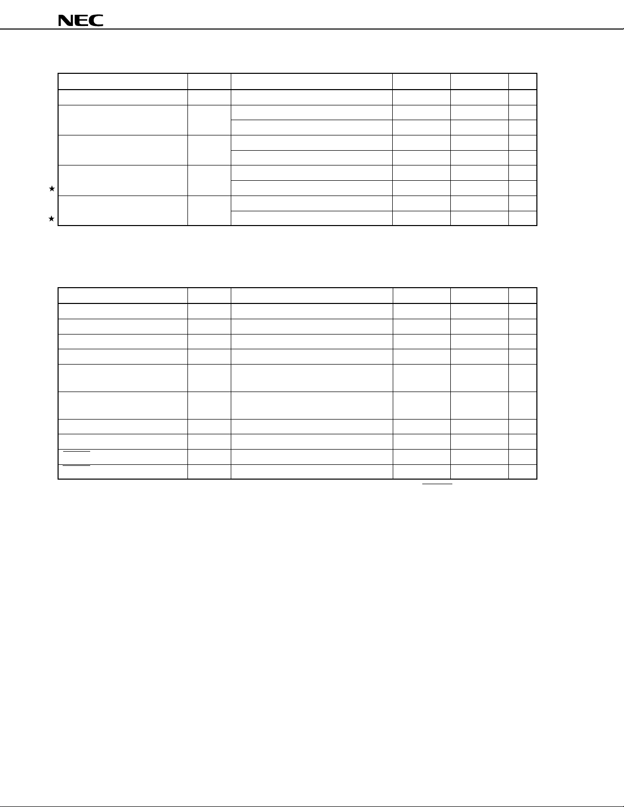
µ
PD784907, 784908
Clock Output Operation (TA = –40 to +85°C, VDD = AVDD = 3.5 to 5.5 V, AVSS = VSS = 0 V)
Parameter Symbol Conditions MIN. MAX. Unit
CLKOUT cycle time tCYCL nT 79 32,000 ns
CLKOUT low-level width tCLL VDD = 4.0 to 5.5 V, 0.5T – 10 30 ns
0.5T – 20 20 ns
CLKOUT high-levell width tCLH VDD = 4.0 to 5.5 V, 0.5T – 10 30 ns
0.5T – 20 20 ns
CLKOUT rising time tCLR VDD = 4.0 to 5.5 V 10 ns
VDD = 3.5 to 4.0 V 0.3 20 ns
CLKOUT falling time t CLF VDD = 4.0 to 5.5 V 10 ns
V
DD = 3.5 to 4.0 V 0.3 20 ns
Remark n: Dividing ratio set by software in the CPU (n = 1, 2, 4, 8, and 16)
CYK (system clock cycle time)
T: t
Other Operations (T
Parameter Symbol Conditions MIN. MAX. Unit
NMI low-level width tWNIL 10
NMI high-level width tWNIH 10
INTP0 low-level width tWIT0L 4tCYSMP ns
INTP0 high-level width tWIT0H 4tCYSMP ns
INTP1 to INTP3 and CI tWIT1L 4tCYCPU ns
low-level width
INTP1 to INTP3 and CI t
high-level width
INTP4 and INTP5 low-level width tWIT2L 10
INTP4 and INTP5 high-level width tWIT2H 10
RESET low-level width
RESET high-level width t
A = –40 to +85°C, VDD = AVDD = 3.5 to 5.5 V, AVSS = VSS = 0 V)
WIT1H 4tCYCPU ns
Note
tWRSL 10
WRSH 10
Note When the power is ON, secure the oscillation stabilization wait time with the RESET low-level width.
Remark t
CYSMP: sampling clock set by software
CYCPU: CPU operation clock set by software in the CPU
t
µ
s
µ
s
µ
s
µ
s
µ
s
µ
s
80
Data Sheet U11680EJ2V0DS00
Page 81
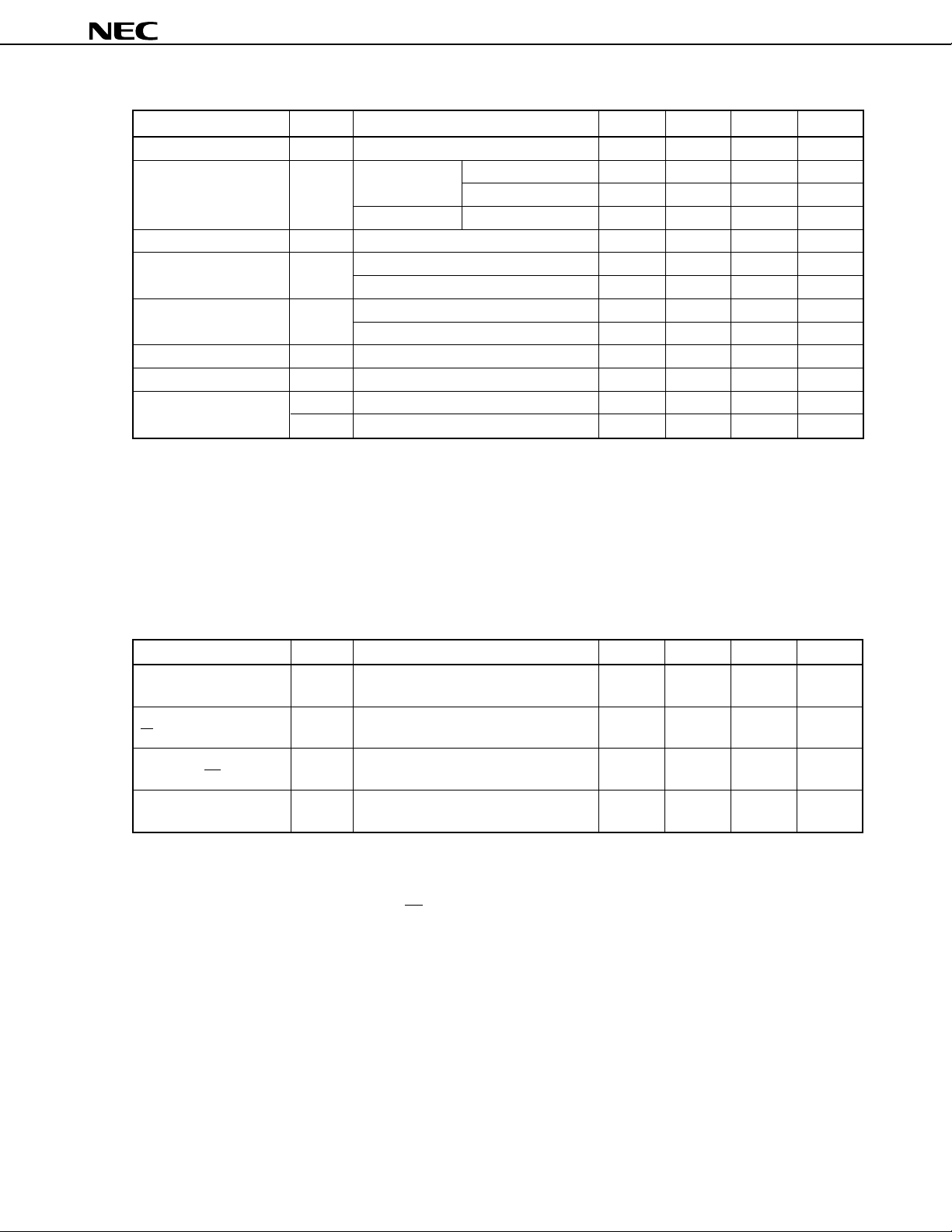
µ
PD784907, 784908
A/D Converter Characteristics (TA = –40 to +85°C, VDD = AVDD = AVREF1 = 3.5 to 5.5 V, VSS = AVSS = 0 V)
Parameter Symbol Conditions MIN. TYP. MAX. Unit
Resolution 8 bit
Total error
Quantization error ±1/2 LSB
Conversion time tCONV FR = 1 120/fCLK 9.5 480
Sampling time tSAMP FR = 1 18/fCLK 1.4 72
Analog input impedance RAN 1,000 MΩ
AVREF1 impedance RREF1 310 kΩ
AVDD power supply current AIDD1 CS = 1 2.0 5.0 mA
Note
IEAD = 00H 0.6 %
FR = 1 1.5 %
IEAD = 01H VDD = 4.5 to 5.5 V 1 2.2 %
FR = 0 240/fCLK 19.1 960
FR = 0 36/fCLK 2.9 144
AIDD2 CS = 0, STOP mode 1.0 20
µ
s
µ
s
µ
s
µ
s
µ
A
Note Quantization error is not included. This parameter is indicated as the ratio to the full-scale value.
Caution To execute the conversion by the A/D converter set port 7, multiplexed with the A/D input lines,
to output mode to prevent data from being inverted.
Remark f
CLK: system clock frequency (selectable from fXX, fXX/2, fXX/4, and fXX/8 by the standby control register
(STBC))
IEBus Controller Characteristics (T
Parameter Symbol Conditions MIN. TYP. MAX. Unit
IEBus standard fS Transfer speed: mode 1 6.20 6.29 6.39 MHz
frequency
Driver delay time (from tDTX C L = 50 pF
TX output to bus line)
Receiver delay time (from tDRX 0.7
bus line to RX input)
Transmission delay on tDBUS 0.85
bus
Note 1
Note 2
Note 2
Note 2
A = –40 to +85°C, VDD = AVDD = AVREF1 = 4.5 to 5.5 V, AVSS = VSS = 0 V)
Note 3
1.5
Notes 1. The value conforms to the IEBus standard. The IEBus controller is operable within the range of the
oscillator frequency of oscillator characteristics.
2. IEBus system clock: The value is measured when f
X = 6.29 MHz.
3. C is the load capacitance of TX output line.
µ
s
µ
s
µ
s
Data Sheet U11680EJ2V0DS00 81
Page 82
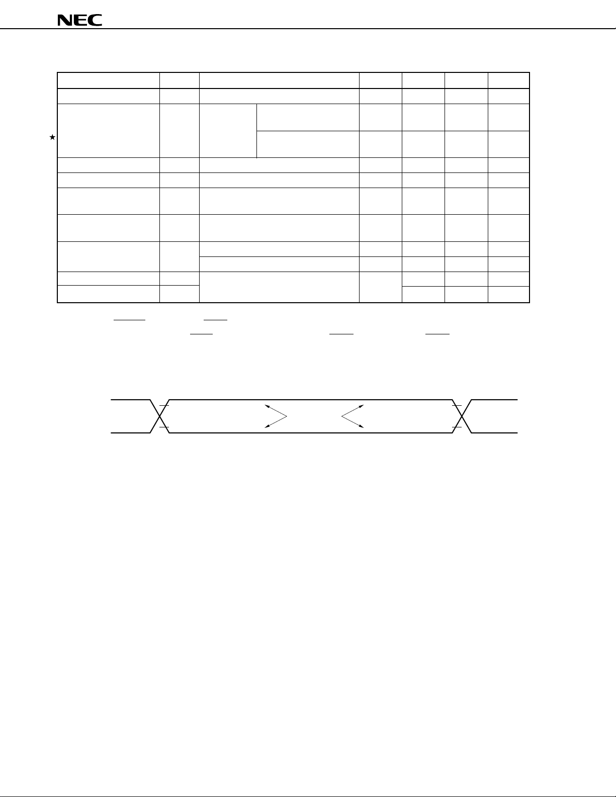
µ
PD784907, 784908
Data Retention Characteristics (TA = –40 to +85°C)
Parameter Symbol Conditions MIN. TYP. MAX. Unit
Data retention voltage VDDDR STOP mode 2.5 5.5 V
Data retention current IDDDR STOP mode VDDDR = 2.5 V, 2 10
AVREF = 0 V
VDDDR = 3.5 to 5.5 V, 10 50
AVREF = 0 V
VDD rising time tRVD 200
VDD falling time tFVD 200
VDD hold time tHVD 0 0.6 ms
(from STOP mode setting)
STOP clear signal tDREL 0ms
input time
Oscillation settling time tWAIT Crystal resonator 30 ms
Ceramic resonator 5 0.1VDDDR ms
Input low voltage VIL Specific pins
Input high voltage VIH 0.9VDDDR V
Note 2
Note 1
Note 1
0VDDDR V
µ
A
µ
A
µ
s
µ
s
Notes 1. Valid when input voltages to the pins described in Note 2 satisfy VIL or VIH in the above table.
2. RESET, P12/ASCK2/SCK2, P20/NMI, P21/INTP0, P22/INTP1, P23/INTP2/CI, P24/INTP3,
P25/INTP4/ASCK/SCK1, P26/INTP5, P27/SI0, P32/SCK0, P33/SO0, P105/SCK3, P106/SI3, and
P107/SO3 pins
AC Timing Test Points
V
DD
– 1 V
0.45 V
0.8 VDD or 2.2 V
0.8 V
0.8 VDD or 2.2 V
Test points
0.8 V
82
Data Sheet U11680EJ2V0DS00
Page 83
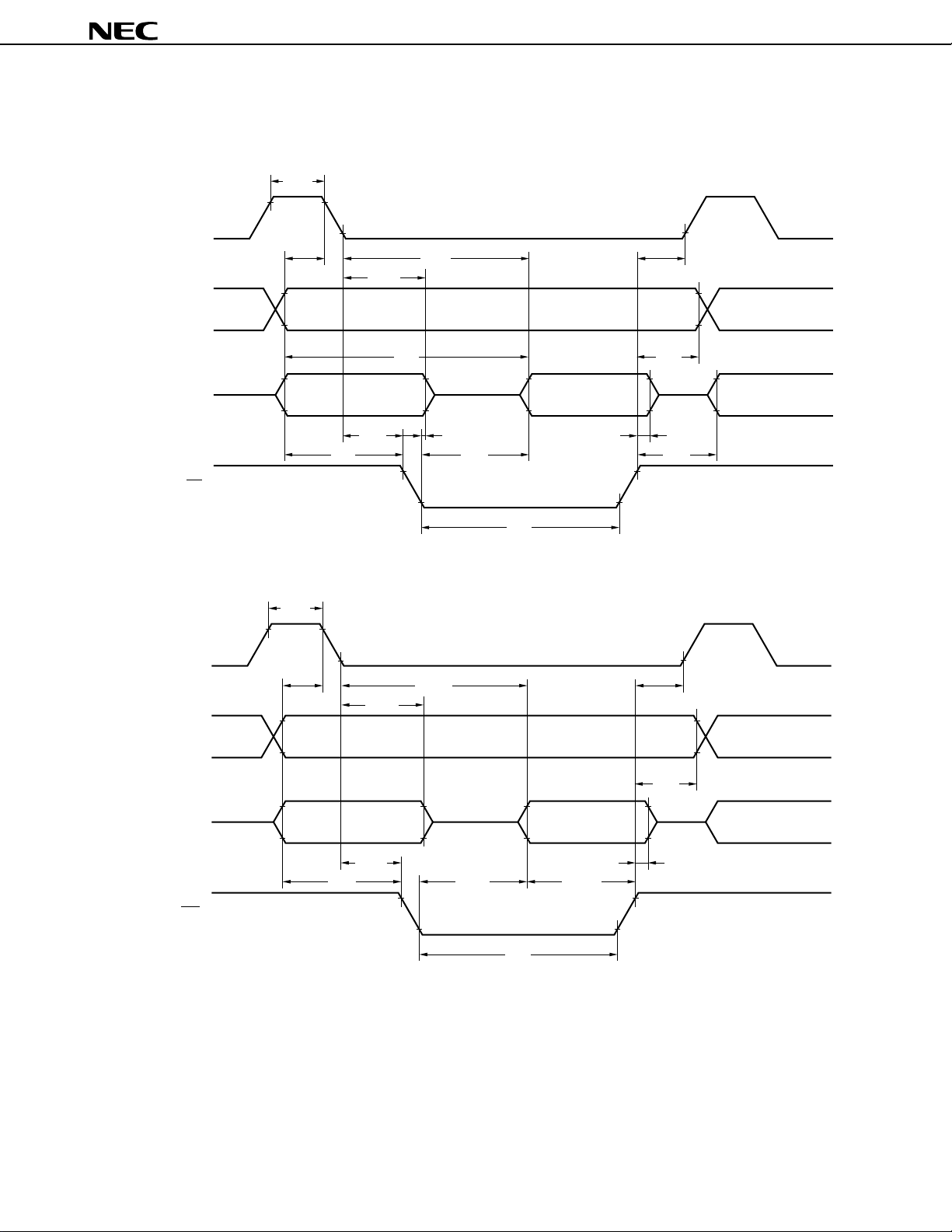
Timing Waveform
(1) Read operation
ASTB
A8 to A19
AD0 to AD7
t
WSTH
t
SAST
t
DAR
t
DSTR
t
HSTLA
t
DAID
t
DSTID
µ
PD784907, 784908
t
DRST
t
HRA
t
FRA
t
DRID
t
HRID
t
DRA
RD
(2) Write operation
ASTB
A8 to A19
AD0 to AD7
WR
t
WSTH
t
SAST
t
DAW
t
DSTW
t
HSTLA
t
DSTOD
t
DWOD
t
WRL
t
SODWR
t
DWST
t
HWA
t
HWOD
t
WWL
Data Sheet U11680EJ2V0DS00 83
Page 84
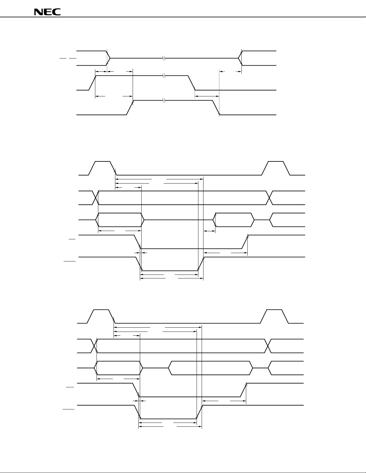
Hold Timing
ASTB, A8 to A19,
AD0 to AD7, RD, WR
t
FHQC
HLDRQ
t
DHQHHAH
HLDAK
External Wait Signal Input Timing
(1) Read operation
ASTB
t
DCFHA
t
DSTWT
t
DSTWTH
t
HSTWTH
t
DHQLHAL
t
DHAC
µ
PD784907, 784908
A8 to A19
AD0 to AD7
RD
WAIT
(2) Write operation
ASTB
A8 to A19
AD0 to AD7
t
DAWT
t
DSTWT
t
DRWTL
t
DSTWTH
t
HSTWTH
t
HRWT
t
DRWTH
t
DWTID
t
DWTR
84
WR
WAIT
t
DAWT
t
DWWTL
t
HWWT
t
DWWTH
Data Sheet U11680EJ2V0DS00
t
DWTW
Page 85
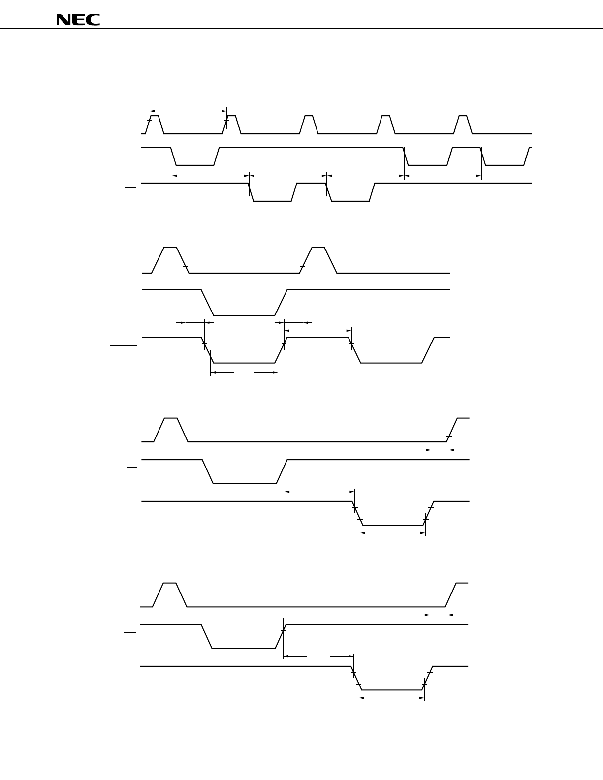
Refresh Timing Waveform
(1) Random read/write cycle
t
RC
ASTB
WR
t
RC
t
RC
t
RC
RD
(2) When refresh memory is accessed for a read and write at the same time
ASTB
RD, WR
µ
PD784907, 784908
t
RC
REFRQ
(3) Refresh after a read
ASTB
RD
REFRQ
(4) Refresh after a write
ASTB
t
DSTRFQ
t
WRFQL
t
t
WRFQH
t
DRRFQ
DRFQST
t
WRFQL
t
DRFQST
WR
REFRQ
tDRFQST
tDWRFQ
tWRFQL
Data Sheet U11680EJ2V0DS00 85
Page 86
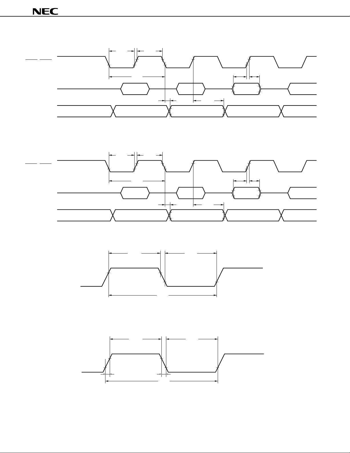
Serial Operation (CSI, CSI3)
SCK0, SCK3
t
WSKL0
t
CYSK0
t
WSKH0
µ
PD784907, 784908
SSSK0tHSSK0
t
SI0, SI3
SO0, SO3
Serial Operation (IOE1, IOE2)
SCK1, SCK2
SI1, SI2
SO1, SO2
Serial Operation (UART, UART2)
t
WSKL1
t
CYSK1
t
WASKH
t
WSKH1
t
DSBSK1
Output data
t
DSOSK
Output data
t
WASKL
t
HSBSK1
t
HSOSK
Input data
SSSK1tHSSK1
t
Input data
ASCK,
ASCK2
Clock Output Timing
CLKOUT
86
t
CLR
t
CYASK
t
CLH
t
CLF
t
CYCL
Data Sheet U11680EJ2V0DS00
t
CLL
Page 87
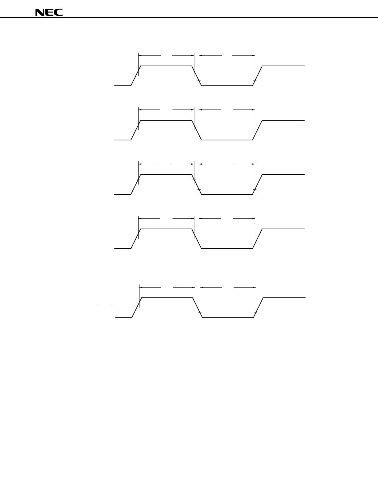
Interrupt Request Input Timing
NMI
INTP0
t
WNIH
t
WIT0H
t
WIT1H
t
WNIL
t
WIT0L
t
WIT1L
µ
PD784907, 784908
INTP1 to INTP3
INTP4, INTP5
Reset Input Timing
RESET
CI,
t
WIT2H
t
WRSH
t
WIT2L
t
WRSL
Data Sheet U11680EJ2V0DS00 87
Page 88
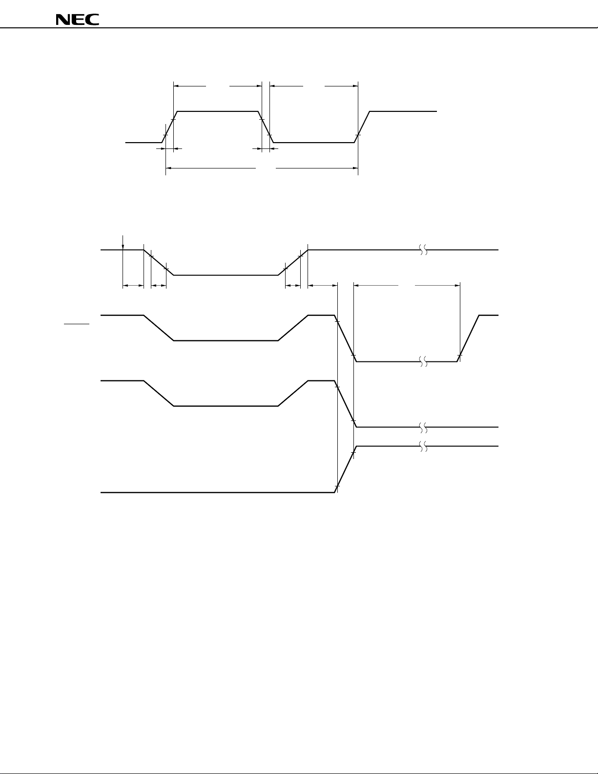
External Clock Timing
X1
Data Retention Characteristics
STOP mode setting
V
DD
t
HVD
t
FVD
µ
PD784907, 784908
t
WXH
t
XR
t
CYX
V
DDDR
t
RVD
t
WXL
t
XF
t
DREL
t
WAIT
RESET
NMI
(Clearing by falling edge)
NMI
(Clearing by rising edge)
88
Data Sheet U11680EJ2V0DS00
Page 89
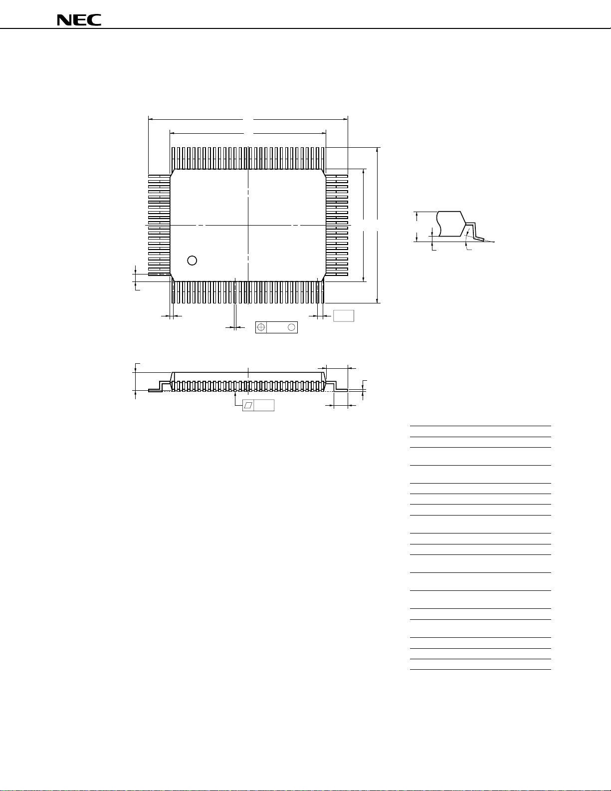
16. PACKAGE DRAWING
100 PIN PLASTIC QFP (14×20)
A
B
µ
PD784907, 784908
81
80
51
50
CD
100
1
30
31
F
G
H
M
I
P
N
NOTE
Each lead centerline is located within 0.15 mm (0.006 inch) of
its true position (T.P.) at maximum material condition.
Remark The shape and material of the ES version are the same
as those of the corresponding mass-produced product.
J
K
L
detail of lead end
S
Q
R
M
ITEM MILLIMETERS INCHES
A 23.6±0.4 0.929±0.016
B 20.0±0.2 0.795
C 14.0±0.2 0.551
D 17.6±0.4 0.693±0.016
F 0.8 0.031
G 0.6 0.024
H 0.30±0.10 0.012
I 0.15 0.006
J 0.65 (T.P.) 0.026 (T.P.)
K 1.8±0.2 0.071
L 0.8±0.2 0.031
M 0.15 0.006
N 0.10 0.004
P 2.7±0.1 0.106
Q 0.1±0.1 0.004±0.004
R5°±5° 5°±5°
S 3.0 MAX. 0.119 MAX.
+0.10
–0.05
P100GF-65-3BA1-3
+0.009
–0.008
+0.009
–0.008
+0.004
–0.005
+0.008
–0.009
+0.009
–0.008
+0.004
–0.003
+0.005
–0.004
Data Sheet U11680EJ2V0DS00 89
Page 90

µ
PD784907, 784908
17. RECOMMENDED SOLDERING CONDITIONS
The µPD784908 should be soldered under the following recommended conditions.
For details of the recommended soldering conditions, refer to the document Semiconductor Device Mounting
Technology Manual (C10535E).
For soldering methods and conditions other than those recommended below, contact your NEC sales represen-
tative.
Table 17-1. Soldering Conditions for Surface Mount Type
µ
PD784907GF-×××-3BA: 100-pin plastic QFP (14 × 20 mm)
µ
PD784908GF-×××-3BA: 100-pin plastic QFP (14 × 20 mm)
Soldering Method Soldering Conditions Recommended Condition
Symbol
Infrared reflow Package peak temperature: 235°C IR35-00-3
Time: 30 seconds max. (210°C or higher)
Count: three times or less
VPS Package peak temperature: 215°C VP15-00-3
Time: 40 seconds or max. (200°C or higher)
Count: three times or less
Wave soldering Solder bath temperature: 260°C max. WS60-00-1
Time: 10 seconds max.
Count : 1
Preheating temperature: 120°C max. (package surface temperature)
Partial heating method Pin temperature: 300°C—
Time: 3 seconds max. (per pin row)
Caution Do not use different soldering methods together (except for partial heating).
90
Data Sheet U11680EJ2V0DS00
Page 91
µ
PD784907, 784908
APPENDIX A DEVELOPMENT TOOLS
The following development tools are available for system development using the µPD784908.
Also refer to (5) Cautions on using development tools.
(1) Language processing software
RA78K4 Assembler package common to 78K/IV Series
CC78K4 C compiler package common to 78K/IV Series
DF784908 Device file for µPD784908 Subseries
CC78K4-L C compiler library source file common to 78K/IV Series
(2) PROM write tools
PG-1500 PROM programmer
PA-78P4908GF Programmer adapter, connects to PG-1500
PG-1500 controller Control program for PG-1500
(3) Debugging tools
• When using the in-circuit emulator IE-78K4-NS
IE-78K4-NS In-circuit emulator common to 78K/IV Series
IE-70000-MC-PS-B Power supply unit for IE-78K4-NS
IE-70000-98-IF-C Interface adapter when a PC-9800 Series computer (except notebook type)
is used as the host machine (C bus supported)
IE-70000-CD-IF-A P C card and interface cable when a notebook type is used as the
host machine (PCMCIA socket supported)
IE-70000-PC-IF-C Interface adapter when an IBM PC/ATTM or compatible is used as the host
machine (ISA bus supported)
IE-70000-PCI-IF Adapter when a PC that incorporates a PCI bus is used as the host machine
IE-784908-NS-EM1 Emulation board to emulate µPD784908 Subseries
NP-100GF
EV-9200GF-100 Socket to be mounted on target system board made for 100-pin plastic QFP
ID78K4-NS Integrated debugger for IE-78K4-NS
SM78K4 System simulator common to 78K/IV Series
DF784908 Device file for µPD784908 Subseries
Note
Emulation probe for 100-pin plastic QFP (GF-3BA type)
(GF-3BA type). Used in LCC mode.
Note Under development
Data Sheet U11680EJ2V0DS00 91
Page 92

µ
PD784907, 784908
• When using the in-circuit emulator IE-784000-R
IE-784000-R In-circuit emulator common to 78K/IV Series
IE-70000-98-IF-C Interface adapter when a PC-9800 Series computer (except notebook type)
is used as the host machine (C bus supported)
IE-70000-PC-IF-C Interface adapter when an IBM PC/AT or compatible is used as the host
machine (ISA bus supported)
IE-70000-PCI-IF Adapter when a PC that incorporates a PCI bus is used as the host machine
IE-78000-R-SV3 Interface adapter and cable when the EWS is used as the host machine
IE-784908-NS-EM1 Emulation board to emulate µPD784908 Subseries
IE-784908-R-EM1
IE-784000-R-EM Emulation board common to 78K/IV Series
IE-78K4-R-EX2 Conversion board for emulation probes required to use the IE-784908-NS-
EM1 on the IE-784000-R. The board is not needed when the conventional
product IE-784908-R-EM1 is used.
EP-78064-GF-R Emulation probe for 100-pin plastic QFP (GF-3BA type)
EV-9200GF-100 Socket to be mounted on target system board made for 100-pin plastic QFP
(GF-3BA type)
ID78K4 Integrated debugger for IE-784000-R
SM78K4 System simulator common to 78K/IV Series
DF784908 Device file for µPD784908 Subseries
(4) Real-time OS
RX78K/IV Real-time OS for 78K/IV Series
MX78K4 OS for 78K/IV Series
92
Data Sheet U11680EJ2V0DS00
Page 93

µ
PD784907, 784908
(5) Cautions on using development tools
• The ID78K4-NS, ID78K4, and SM78K4 are used in combination with the DF784908.
• The CC78K4 and RX78K/IV are used in combination with the RA78K4 and DF784908.
• The NP-100GF is a product made by Naito Densei Machidaseisakusho Co., Ltd. (+81-44-822-3813). Contact
an NEC distributor regarding the purchase of these products.
• The host machines and OSs suitable for each software are as follows.
Host Machine PC EWS
[OS]
Software [Japanese/English Windows] NEWSTM (RISC) [NEWS-OSTM]
RA78K4 √
CC78K4 √
PG-1500 controller √
ID78K4-NS √ —
ID78K4 √√
SM78K4 √ —
RX78K/IV √
MX78K4 √
PC-9800 Series [WindowsTM] HP9000 series 700TM [HP-UXTM]
IBM PC/AT and compatibles SPARCstationTM [SunOSTM, SolarisTM]
Note
Note
Note
Note
Note
√
√
—
√
√
Note DOS-based software
Data Sheet U11680EJ2V0DS00 93
Page 94

µ
PD784907, 784908
APPENDIX B RELATED DOCUMENTS
Documents related to devices
Document Name Document No.
Japanese English
µ
PD784907, 784908 Data Sheet U11680J This manual
µ
PD78P4908 Data Sheet U11681J U11681E
µ
PD784908 Subseries User's Manual Hardware U11787J U11787E
µ
PD784908 Subseries Special Function Register Table U11589J —
78K/IV Series User's Manual Instructions U10905J U10905E
78K/IV Series Instruction Table U10594J —
78K/IV Series Instruction Set U10595J —
78K/IV Series Application Note Software Basics U10095J U10095E
Documents related to development tools (User's Manual)
Document Name Document No.
Japanese English
RA78K4 Assembler Package Language U11162J U11162E
Operation U11334J U11334E
RA78K4 Structured Assembler Preprocessor U11743J U11743E
CC78K4 C Compiler Language U11571J U11571E
Operation U11572J U11572E
PG-1500 PROM Programmer U11940J U11940E
PG-1500 Controller PC-9800 Series (MS-DOSTM) Based EEU-704 EEU-1291
PG-1500 Controller IBM PC Series (PC DOSTM) Based EEU-5008 U10540E
IE-78K4-NS U13356J U13356E
IE-784000-R U12903J U12903E
IE-784908-R-EM1 U11876J —
IE-784908-NS-EM1 U13743J Under preparation
EP-78064 EEU-934 EEU-1469
SM78K4 System Simulator Windows Based Reference U10093J U10093E
SM78K Series System Simulator External Part User Open U10092J U10092E
Interface Specifications
ID78K4-NS Integrated Debugger PC Based Reference U12796J U12796E
ID78K4 Integrated Debugger Windows Based Reference U10440J U10440E
ID78K4 Integrated Debugger HP-UX, SunOS, NEWS-OS Based Reference U11960J U11960E
Caution The above documents may be revised without notice. Use the latest versions when you design
application systems.
94
Data Sheet U11680EJ2V0DS00
Page 95

µ
PD784907, 784908
Documents related to embedded software (User's Manual)
Document Name Document No.
Japanese English
78K/IV Series Real-Time OS Fundamental U10603J U10603E
Installation U10604J U10604E
Debugger U10364J —
78K/IV Series OS MX78K4 Fundamental U11779J —
Other documents
Document Name Document No.
Japanese English
NEC IC PACKAGE MANUAL (CD-ROM) — C13388E
Semiconductor Device Mounting Technology Manual C10535J C10535E
Quality Grades on NEC Semiconductor Device C11531J C11531E
NEC Semiconductor Device Reliability/Quality Control System C10983J C10983E
Guide to Prevent Damage for Semiconductor Devices by Electrostatic Discharge (ESD) C11892J C11892E
Guide to Quality Assurance for Semiconductor Devices — MEI-1202
Guide to Microcontroller-Related Products by Third Parties U11416J —
Caution The above documents may be revised without notice. Use the latest versions when you design
application systems.
Data Sheet U11680EJ2V0DS00 95
Page 96
µ
PD784907, 784908
NOTES FOR CMOS DEVICES
1 PRECAUTION AGAINST ESD FOR SEMICONDUCTORS
Note: Strong electric field, when exposed to a MOS device, can cause destruction of
the gate oxide and ultimately degrade the device operation. Steps must be taken
to stop generation of static electricity as much as possible, and quickly dissipate
it once, when it has occurred. Environmental control must be adequate. When
it is dry, humidifier should be used. It is recommended to avoid using insulators
that easily build static electricity. Semiconductor devices must be stored and
transported in an anti-static container, static shielding bag or conductive
material. All test and measurement tools including work bench and floor should
be grounded. The operator should be grounded using wrist strap. Semiconductor
devices must not be touched with bare hands. Similar precautions need to be
taken for PW boards with semiconductor devices on it.
2 HANDLING OF UNUSED INPUT PINS FOR CMOS
Note: No connection for CMOS device inputs can be cause of malfunction. If no
connection is provided to the input pins, it is possible that an internal input level
may be generated due to noise, etc., hence causing malfunction. CMOS device
behave differently than Bipolar or NMOS devices. Input levels of CMOS devices
must be fixed high or low by using a pull-up or pull-down circuitry. Each unused
pin should be connected to VDD or GND with a resistor, if it is considered to have
a possibility of being an output pin. All handling related to the unused pins must
be judged device by device and related specifications governing the devices.
3 STATUS BEFORE INITIALIZATION OF MOS DEVICES
Note: Power-on does not necessarily define initial status of MOS device. Production
process of MOS does not define the initial operation status of the device.
Immediately after the power source is turned ON, the devices with reset function
have not yet been initialized. Hence, power-on does not guarantee out-pin
levels, I/O settings or contents of registers. Device is not initialized until the
reset signal is received. Reset operation must be executed immediately after
power-on for devices having reset function.
96
Data Sheet U11680EJ2V0DS00
Page 97

µ
Regional Information
Some information contained in this document may vary from country to country. Before using any NEC
product in your application, pIease contact the NEC office in your country to obtain a list of authorized
representatives and distributors. They will verify:
•
Device availability
•
Ordering information
•
Product release schedule
•
Availability of related technical literature
•
Development environment specifications (for example, specifications for third-party tools and
components, host computers, power plugs, AC supply voltages, and so forth)
•
Network requirements
In addition, trademarks, registered trademarks, export restrictions, and other legal issues may also vary
from country to country.
NEC Electronics Inc. (U.S.)
Santa Clara, California
Tel: 408-588-6000
800-366-9782
Fax: 408-588-6130
800-729-9288
NEC Electronics (Germany) GmbH
Duesseldorf, Germany
Tel: 0211-65 03 02
Fax: 0211-65 03 490
NEC Electronics (UK) Ltd.
Milton Keynes, UK
Tel: 01908-691-133
Fax: 01908-670-290
NEC Electronics Italiana s.r.l.
Milano, Italy
Tel: 02-66 75 41
Fax: 02-66 75 42 99
NEC Electronics (Germany) GmbH
Benelux Office
Eindhoven, The Netherlands
Tel: 040-2445845
Fax: 040-2444580
NEC Electronics (France) S.A.
Velizy-Villacoublay, France
Tel: 01-30-67 58 00
Fax: 01-30-67 58 99
NEC Electronics (France) S.A.
Spain Office
Madrid, Spain
Tel: 01-504-2787
Fax: 01-504-2860
NEC Electronics (Germany) GmbH
Scandinavia Office
Taeby, Sweden
Tel: 08-63 80 820
Fax: 08-63 80 388
NEC Electronics Hong Kong Ltd.
Hong Kong
Tel: 2886-9318
Fax: 2886-9022/9044
NEC Electronics Hong Kong Ltd.
Seoul Branch
Seoul, Korea
Tel: 02-528-0303
Fax: 02-528-4411
NEC Electronics Singapore Pte. Ltd.
United Square, Singapore 1130
Tel: 65-253-8311
Fax: 65-250-3583
NEC Electronics Taiwan Ltd.
Taipei, Taiwan
Tel: 02-2719-2377
Fax: 02-2719-5951
NEC do Brasil S.A.
Electron Devices Division
Rodovia Presidente Dutra, Km 214
07210-902-Guarulhos-SP Brasil
Tel: 55-11-6465-6810
Fax: 55-11-6465-6829
J98. 11
PD784907, 784908
Data Sheet U11680EJ2V0DS00 97
Page 98

µ
PD784907, 784908
FIP, IEBus, and EEPROM are trademarks of NEC Corporation.
MS-DOS and Windows are either registered trademarks or trademarks of Microsoft Corporation in the
United States and/or other countries.
PC/AT and PC DOS are trademarks of International Business Machines Corporation.
HP9000 series 700 and HP-UX are trademarks of Hewlett-Packard Company.
SPARCstation is a trademark of SPARC International, Inc.
Solaris and SunOS are trademarks of Sun Microsystems, Inc.
NEWS and NEWS-OS are trademarks of Sony Corporation.
The related documents in this publication may include preliminary version. However, what preliminary versions
are not marked as such.
The export of this product from Japan is regulated by the Japanese government. To export this product may be prohibited
without governmental license, the need for which must be judged by the customer. The export or re-export of this product
from a country other than Japan may also be prohibited without a license from that country. Please call an NEC sales
representative.
No part of this document may be copied or reproduced in any form or by any means without the prior written
consent of NEC Corporation. NEC Corporation assumes no responsibility for any errors which may appear in this
document.
NEC Corporation does not assume any liability for infringement of patents, copyrights or other intellectual
property rights of third parties by or arising from use of a device described herein or any other liability arising
from use of such device. No license, either express, implied or otherwise, is granted under any patents,
copyrights or other intellectual property rights of NEC Corporation or others.
While NEC Corporation has been making continuous effort to enhance the reliability of its semiconductor devices,
the possibility of defects cannot be eliminated entirely. To minimize risks of damage or injury to persons or
property arising from a defect in an NEC semiconductor device, customers must incorporate sufficient safety
measures in its design, such as redundancy, fire-containment, and anti-failure features.
NEC devices are classified into the following three quality grades:
"Standard", "Special", and "Specific". The Specific quality grade applies only to devices developed based on
a customer designated "quality assurance program" for a specific application. The recommended applications
of a device depend on its quality grade, as indicated below. Customers must check the quality grade of each
device before using it in a particular application.
Standard: Computers, office equipment, communications equipment, test and measurement equipment,
audio and visual equipment, home electronic appliances, machine tools, personal electronic
equipment and industrial robots
Special: Transportation equipment (automobiles, trains, ships, etc.), traffic control systems, anti-disaster
systems, anti-crime systems, safety equipment and medical equipment (not specifically designed
for life support)
Specific: Aircrafts, aerospace equipment, submersible repeaters, nuclear reactor control systems, life
support systems or medical equipment for life support, etc.
The quality grade of NEC devices is "Standard" unless otherwise specified in NEC's Data Sheets or Data Books.
If customers intend to use NEC devices for applications other than those specified for Standard quality grade,
they should contact an NEC sales representative in advance.
Anti-radioactive design is not implemented in this product.
Data Sheet U11680EJ2V0DS00
M4 96. 5
 Loading...