

Page 1
DATA SHEET
MOS INTEGRATED CIRCUIT
µ
PD78081(A), 78082(A)
8-BIT SINGLE-CHIP MICROCONTROLLER
DESCRIPTION
The µPD78081(A) and 78082(A) are members of the µPD78083 Subseries of the 78K/0 Series microcontrollers.
µ
These products are produced with a more stringent quality assurance program than that of the
78082 (standard models) (NEC classifies these products as “special products” by quality grade).
Besides a high-speed, high-performance CPU, these microcontrollers have on-chip ROM, RAM, I/O ports,
8-bit resolution A/D converter, timer, serial interface, interrupt control, and other peripheral hardware.
µ
PD78P083(A) including a one-time PROM version which can operate in the same power supply voltage
The
range as a mask ROM version, and various development tools are available.
PD78081 and
The details of the functions are described in the following User’s Manuals. Be sure to read the documents before
starting design.
µ
PD78083 Subseries User’s Manual : IEU-1407
78K/0 Series User’s Manual Instructions : IEU-1372
FEATURES
• Internal ROM and RAM
Item
Part Number
µ
PD78081(A) 8 Kbytes 256 bytes 44-pin plastic QFP (10 × 10 mm)
µ
PD78082(A) 16 Kbytes 384 bytes
• Minimum instruction execution time can be changed from high-speed (0.4
Program Memory Data Memory
(ROM) (Internal High-speed RAM)
Package
µ
s) to low-speed (12.8 µs)
• I/O ports: 33
• 8-bit resolution A/D converter : 8 channels
• Serial interface : 1 channel
3-wire serial I/O/UART
mode : 1 channel
• Timer : 3 channels
• Supply voltage : VDD = 1.8 to 5.5 V
APPLICATION FIELDS
Controllers for automobile electronic control systems, gas detector circuit-breakers, various types of safety
equipment, etc.
µ
In addition to the
specified, however, the
products, and their descriptions also apply to the
Document No. U12436EJ1V0DS00 (1st edition)
Date Published July 1997 N
Printed in Japan
PD78081(A) and 78082(A), this Data Sheet also describes the µPD78081(A2). Unless otherwise
µ
PD78081(A) and 78082(A) are used throughout this Data Sheet as the representative
µ
PD78081(A2).
The information in this document is subject to change without notice.
©
1997
Page 2
ORDERING INFORMATION
Part Number Package
µ
PD78081GB(A)-×××-3B4 44-pin plastic QFP (10 × 10 mm)
µ
PD78081GB(A)-×××-3BS-MTX
µ
PD78082GB(A)-×××-3B4 44-pin plastic QFP (10 × 10 mm)
µ
PD78082GB(A)-×××-3BS-MTX
µ
PD78081GB(A2)-×××-3B4 44-pin plastic QFP (10 × 10 mm)
Note Under planning
Note
44-pin plastic QFP (10 × 10 mm)
Note
44-pin plastic QFP (10 × 10 mm)
µ
PD78081(A), 78082(A)
Caution
µ
PD78081GB(A) and 78082GB(A) have two kinds of package (Refer to 11. PACKAGE DRAWINGS).
Please consult NEC’s sales representative for the available package.
Remark ××× indicates ROM code suffix.
QUALITY GRADE
Special
Please refer to “Quality Grades on NEC Semiconductor Devices” (Document No. C11531E) published by
NEC Corporation to know the specification of quality grade on the devices and its recommended applications.
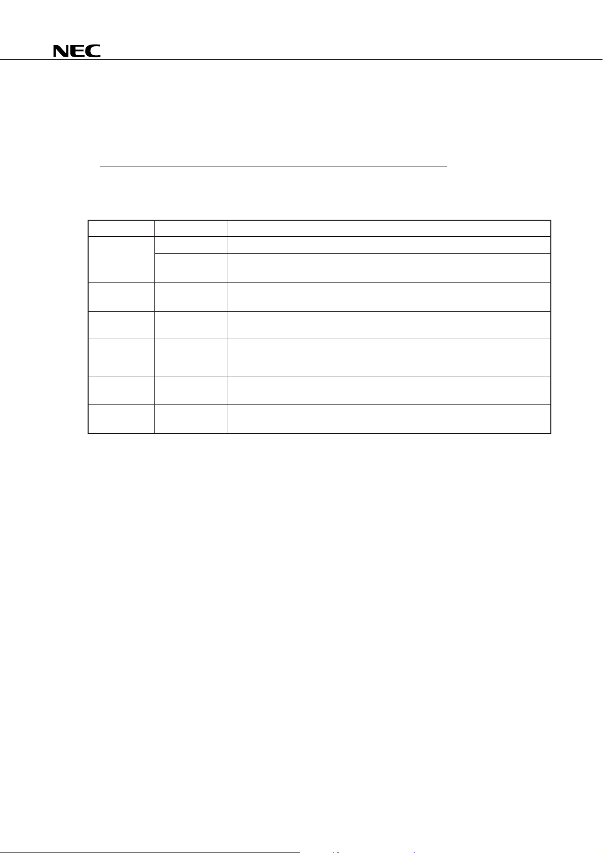
DIFFERENCES BETWEEN µPD78081 AND 78082, AND µPD78081(A) AND 78082(A)
Part Number
Item
Quality grade Standard Special
Package • 42-pin plastic shrink DIP (600 mil) 44-pin plastic QFP (10 × 10 mm)
• 44-pin plastic QFP (10 × 10 mm)
µ
PD78081, 78082
µ
PD78081(A), 78082(A)
DIFFERENCES BETWEEN µPD78081(A) AND 78081(A2)
Part Number
Item
Supply voltage VDD = 1.8 to 5.5 V VDD = 5 V ±10%
Minimum instruction execution 0.4 µs (at 5 MHz) 0.57 µs (at 7 MHz)
time
Operating ambient temperature TA = –40 to 85˚C TA = –40 to +125˚C
Remark In addition to the above parameters, the supply current also differs. For details, refer to 10. ELECTRICAL
SPECIFICATIONS.
µ
PD78081(A)
µ
PD78081(A2)
2
Page 3
µ
PD78014
PD78002
PD78083
PD78002Y
100-pin
100-pin
100-pin
64-pin
64-pin
64-pin
42/44-pin
Control
Y subseries products are compatible with I
2
C bus.
A timer was added to the PD78054, and the external interface function was enhanced.
EMI noise reduction version of the PD78078.
ROM-less versions of the PD78078.
An A/D converter and 16-bit timer were added to the PD78002.
An A/D converter was added to the PD78002.
Basic subseries for control.
On-chip UART, capable of operating at a low voltage (1.8 V).
PD780018AY
100-pin Serial I/O of the PD78078Y was enhanced, and only selected functions are provided.
PD78078
PD78070A
PD78075B
PD78070AY
µ
µ
µµ
µ
µµ
µ
µµ
µ
µ
µ
µ
µ
µ
Inverter control
PD78096464-pin
µ
An A/D converter of the PD780924 was enhanced.
PD78078Y
µ
µ
PD78075BY
PD78018F
PD780001
PD78018FY
PD78014Y
80-pin
80-pin
64-pin
78K/0
Series
Products in mass production
Products under development
EMI noise reduction version of the PD78054.
UART and D/A converter were added to the PD78014, and I/O was enhanced.
Low-voltage (1.8 V) operation versions of the PD78014 with several ROM and RAM capacities available.
An A/D converter of the PD780024 was enhanced.
EMI noise reduction version of the PD78018F.
On-chip inverter control circuit and UART, EMI noise reduction version.
Serial I/O of the PD78018F was enhanced, EMI noise reduction version.
Serial I/O of the PD78054 was enhanced, EMI noise reduction version.
PD78005880-pin
µ
µµ
PD780034
PD780024
PD78014H
PD780034Y
PD780024Y
64-pin
64-pin
64-pin
µµ
µµ
µ
µ
µ
µ
µ
µ
µ
µ
µ
FIPTM drive
PD78044F
100-pin
80-pin
80-pin
µ
µ
The I/O and FIP C/D of the PD78044F were enhanced, Display output total: 53
The I/O and FIP C/D of the PD78044H were enhanced, Display output total: 48
N-ch open-drain input/output was added to the PD78044F, Display output total: 34
Basic subseries for driving FIP, Display output total: 34
µ
µ
100-pin
PD78092464-pin
µ
PD780308
PD78064B
PD78064
100-pin
100-pin
100-pin
µ
µ
SIO of the PD78064 was enhanced, and ROM and RAM were expanded.
EMI noise reduction version of the PD78064.
Basic subseries for driving LCDs, On-chip UART.
µ
PD780308Y
µ
PD78064Y
µ
LCD drive
µ
µ
LV
PD78P0914
64-pin
µ
On-chip PWM output, LV digital code decoder, Hsync counter.
PD78054
µ
PD78054Y
µ
PD78058FY
µ
PD780058Y
Note
µ
PD78058F
µ
PD78044H
µ
µ
PD780228
PD780208
µ
µ
µ
IEBusTM supported
PD78098B80-pin
µ
EMI noise reduction version of the PD78098.
The IEBus controller was added to the PD78054.
PD7809880-pin
µ
µ
Meter control
PD780973
80-pin
µ
On-chip automobile meter driving controller/driver.
PD78081(A), 78082(A)
78K/0 SERIES DEVELOPMENT
The following shows the 78K/0 Series products development. Subseries names are shown inside frames.
Note Under planning
3
Page 4
The following table shows the differences among subseries functions.
µ
PD78081(A), 78082(A)
Function ROM Timer 8-bit
Subseries Name
ControlµPD78075B
µ
PD78078
µ
PD78070A – 61 2.7 V
µ
PD780058
µ
PD78058F
µ
PD78054
µ
PD780034
µ
PD780024 8ch –
µ
PD78014H 2ch 53
µ
PD78018F
µ
PD78014
µ
PD780001 8 K – – 1ch 39 –
µ
PD78002
µ
PD78083 – 8ch 1ch (UART: 1ch) 33 1.8 V –
InverterµPD780964
controlµPD780924 8ch –
FIP
drive
LCD
drive
IEBus
supportedµPD78098
Meter
control
LV
µ
PD780208
µ
PD780228
µ
PD78044H
µ
PD78044F
µ
PD780308
µ
PD78064B 32 K 2ch (UART: 1ch)
µ
PD78064
µ
PD78098B
µ
PD780973
µ
PD78P0914
Capacity 8-bit 16-bit Watch WDT A/D A/D D/A
32 K to 40 K
48 K to 60 K
24 K to 60 K
48 K to 60 K
16 K to 60 K
8 K to 32 K
8 K to 60 K
8 K to 32 K
8 K to 16 K
8 K to 32 K
32 K to 60 K
48 K to 60 K
32 K to 48 K
16 K to 40 K
48 K to 60 K
16 K to 32 K
40 K to 60 K
32 K to 60 K
24 K to 32 K
32 K 6ch – – 1ch 8ch – – 2ch 54 4.5 V
4ch 1ch 1ch 1ch 8ch – 2ch 3ch (UART: 1ch) 88 1.8 V
2ch 2ch
1ch – 53
3ch Note – 1ch – 8ch – 2ch (UART: 2ch) 47 2.7 V
2ch 1ch 1ch 1ch 8ch – – 2ch 74 2.7 V –
3ch – – 1ch 72 4.5 V
2ch 1ch 1ch 68 2.7 V
2ch 1ch 1ch 1ch 8ch – –
2ch 1ch 1ch 1ch 8ch – 2ch 3ch (UART: 1ch) 69 2.7 V
3ch 1ch 1ch 1ch 5ch – – 2ch (UART: 1ch) 56 4.5 V –
10-bit
– 8ch – 3ch (UART: 1ch, 51 1.8 V
8-bit Serial Interface I/O VDD
3ch (time-division UART: 1ch)
3ch (UART: 1ch) 69 2.7 V
time-division 3-wire: 1ch)
2ch
3ch (time-division UART: 1ch)
MIN.
Value
68 1.8 V
2.0 V
2.7 V
57 2.0 V –
External
Expansion
Available
Available
Available
Available
Available
Note 10-bit timer: 1 channel
4
Page 5
OVERVIEW OF FUNCTION
µ
PD78081(A), 78082(A)
Part Number
Item
Internal
memory
Memory space
General registers
Minimum instruction execution time
Instruction set
I/O ports
A/D converter
Serial interface
Timer
Timer output
Clock output
Buzzer output
Vectored
interrupt
sources
Supply voltage
Operating ambient temperature
Package
ROM
Internal high-speed RAM
Maskable
Non-maskable
Software
µ
µ
PD78081(A)
8 Kbytes
256 bytes
64 Kbytes
8 bits × 32 registers (8 bits × 8 registers × 4 banks)
On-chip minimum instruction execution time selective function
0.4 µs/0.8 µs/1.6 µs/3.2 µs/6.4 µs/12.8 µs (at main system clock of 5.0 MHz)
• 16-bit operation
• Multiply/divide (8 bits × 8 bits,16 bits ÷ 8 bits)
• Bit manipulation (set, reset, test, boolean operation)
• BCD adjustment, etc.
Total : 33
• CMOS input : 01
• CMOS I/O : 32
8-bit resolution × 8 channels
3-wire serial I/O/UART mode selectable : 1 channel
• 8-bit timer/event counter : 2 channels
• Watchdog timer : 1 channel
2 (8-bit PWM output)
19.5 kHz, 39.1 kHz, 78.1 kHz, 156 kHz, 313 kHz, 625 kHz, 1.25 MHz, 2.5 MHz,
5.0 MHz (at main system clock of 5.0 MHz)
1.2 kHz, 2.4 kHz, 4.9 kHz, 9.8 kHz (at main system clock of 5.0 MHz)
Internal : 8, external : 3
Internal : 1
1
DD = 1.8 to 5.5 V
V
A = –40 to +85°C
T
44-pin plastic QFP (10 × 10 mm)
16 Kbytes
384 bytes
PD78082(A)
Caution The supply voltage and other parameters of the µPD78081(A2) differ from those of the other models.
µ
For details, refer to “DIFFERENCES BETWEEN
PD78081(A) AND 78081(A2)”.
5
Page 6

µ
PD78081(A), 78082(A)
CONTENTS
1. PIN CONFIGURATION (Top View) ................................................................................................... 7
2. BLOCK DIAGRAM ............................................................................................................................. 9
3. PIN FUNCTIONS .............................................................................................................................. 10
3.1 Port Pins................................................................................................................................................... 10
3.2 Non-port Pins .......................................................................................................................................... 11
3.3 Pin I/O Circuits and Recommended Connection of Unused Pins ................................................... 12
4. MEMORY SPACE............................................................................................................................. 14
5. PERIPHERAL HARDWARE FUNCTIONS ...................................................................................... 15
5.1 Ports..........................................................................................................................................................15
5.2 Clock Generator ......................................................................................................................................16
5.3 Timer/Event Counter...............................................................................................................................16
5.4 Clock Output Control Circuit................................................................................................................. 18
5.5 Buzzer Output Control Circuit .............................................................................................................. 18
5.6 A/D Converter .......................................................................................................................................... 19
5.7 Serial Interface ........................................................................................................................................ 20
6. INTERRUPT FUNCTIONS ............................................................................................................... 21
7. STANDBY FUNCTION ..................................................................................................................... 24
8. RESET FUNCTION........................................................................................................................... 24
9. INSTRUCTION SET.......................................................................................................................... 25
10. ELECTRICAL SPECIFICATIONS.................................................................................................... 28
11. PACKAGE DRAWINGS ................................................................................................................... 49
12. RECOMMENDED SOLDERING CONDITIONS .............................................................................. 51
APPENDIX A. DEVELOPMENT TOOLS .............................................................................................. 52
APPENDIX B. RELATED DOCUMENTS .............................................................................................. 54
6
Page 7
1. PIN CONFIGURATION (Top View)
• 44-pin plastic QFP (10 × 10 mm)
µ
PD78081GB(A)-×××-3B4
µ
PD78081GB(A)-×××-3BS-MTX
µ
PD78082GB(A)-×××-3B4
µ
PD78082GB(A)-×××-3BS-MTX
µ
PD78081GB(A2)-×××-3B4
P12/ANI2
P13/ANI3
P14/ANI4
P15/ANI5
P16/ANI6
P17/ANI7
P72/ASCK/SCK2
P71/T
X
D/SO2
X
D/SI2
P70/R
P101/TI6/TO6
P100/TI5/TO5
Note
Note
P11/ANI1
44 43 42 41 40 39 38 37 36 35 34
1
2
3
4
5
6
7
8
9
10
11
12 13 14 15 16 17 18 19 20 21 22
SSAVREFAVDD
P10/ANI0
AV
VDDX1
X2ICRESET
NC
33
32
31
30
29
28
27
26
25
24
23
µ
PD78081(A), 78082(A)
P03/INTP3
P02/INTP2
P01/INTP1
P00
P37
P36/BUZ
P35/PCL
P34
P33
P32
NC
SS
P50
P51
P52
P53
P54
V
P55
P56
Note Under planning
Cautions 1. Connect IC (Internally Connected) pin directly to V
2. Connect AV
3. Connect AV
4. Connect NC (Non-connection) pin to V
DD pin to VDD.
SS pin to VSS.
SS for noise protection (It can be left open).
P57
SS.
P30
P31
7
Page 8

µ
PD78081(A), 78082(A)
ANI0 to ANI7 : Analog Input P100, P101 : Port10
ASCK : Asynchronous Serial Clock PCL : Programmable Clock
DD : Analog Power Supply RESET : Reset
AV
REF : Analog Reference Voltage RxD : Receive Data
AV
SS : Analog Ground SCK2 : Serial Clock
AV
BUZ : Buzzer Clock SI2 : Serial Input
IC : Internally Connected SO2 : Serial Output
INTP1 to INTP3 : Interrupt from Peripherals TI5, TI6 : Timer Input
NC : Non-connection TO5, TO6 : Timer Output
P00 to P03 : Port0 TxD : Transmit Data
P10 to P17 : Port1 V
P30 to P37 : Port3 V
DD : Power Supply
SS : Ground
P50 to P57 : Port5 X1, X2 : Crystal (Main System Clock)
P70 to P72 : Port7
8
Page 9
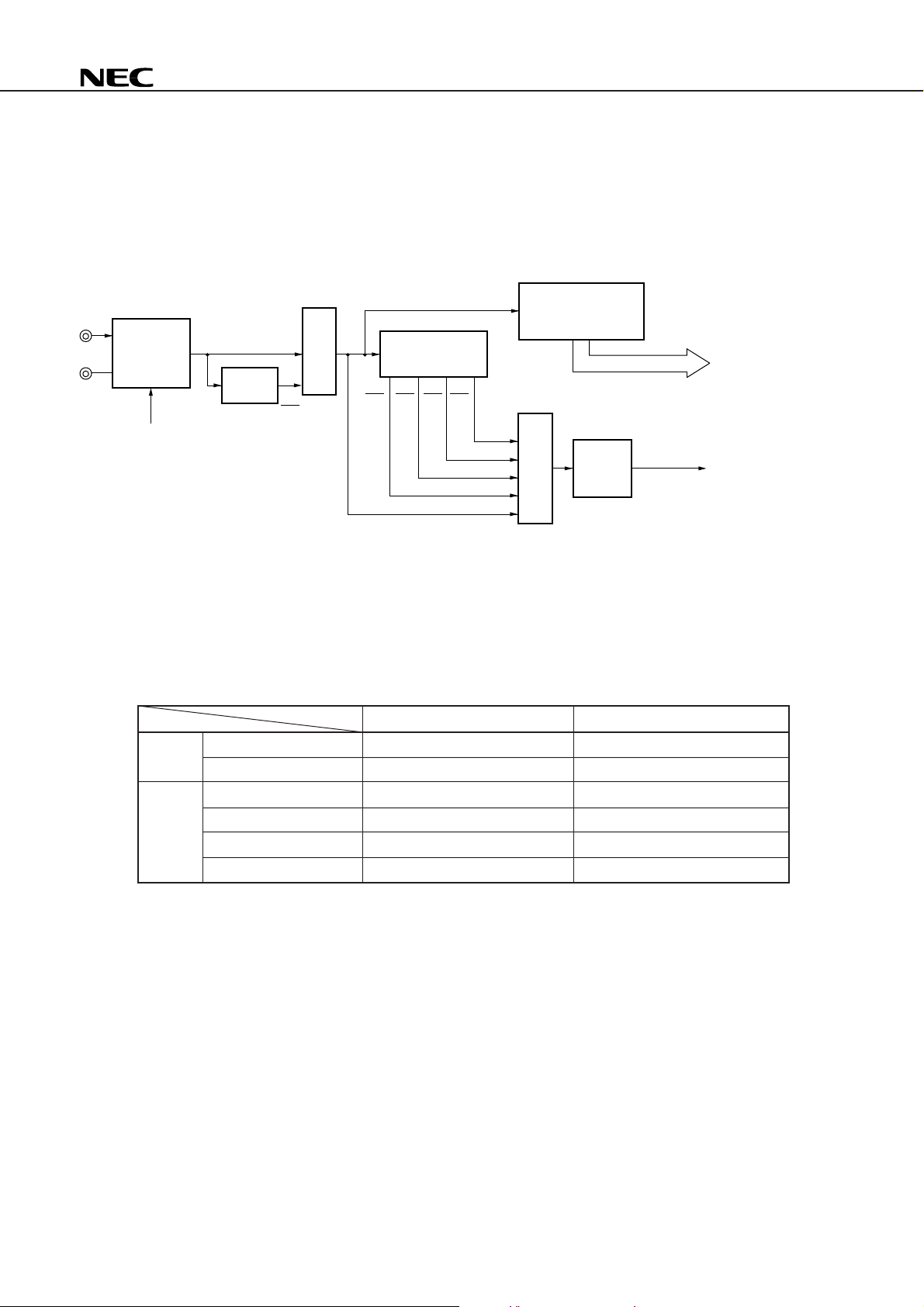
2. BLOCK DIAGRAM
µ
PD78081(A), 78082(A)
P100/TI5/TO5
P101/TI6/TO6
SI2/R
XD/P70
XD/P71
SO2/T
SCK2/ASCK/P72
ANI0/P10 to
ANI7/P17
AV
AVSS
AVREF
INTP1/P01 to
INTP3/P03
BUZ/P36
PCL/P35
8-bit TIMER/
EVENT COUNTER 5
8-bit TIMER/
EVENT COUNTER 6
WATCHDOG
TIMER
SERIAL
INTERFACE 2
DD
A/D
CONVERTER
INTERRUPT
CONTROL
BUZZER OUTPUT
CLOCK OUTPUT
CONTROL
78K/0
CPU
CORE
RAM
VDD VSS
ROM
IC
PORT 0
PORT 1
PORT 3
PORT 5
PORT 7
PORT 10
SYSTEM
CONTROL
P00
P01 to P03
P10 to P17
P30 to P37
P50 to P57
P70 to P72
P100, P101
RESET
X1
X2
Remark The internal ROM and internal high-speed RAM capacities depend on the product.
9
Page 10
µ
PD78081(A), 78082(A)
3. PIN FUNCTIONS
3.1 Port Pins
Pin Name Input/Output Function After Reset Shared by:
P00 Input Port 0 Input only Input —
P01 Input/output 4-bit input/output port Input/output is specifiable Input INTP1
P02 bit-wise. When used as the INTP2
P03 input port, it is possible to INTP3
connect a pull-up resistor by
software.
P10 to P17 Input/output Port 1 Input ANI0 to ANI7
8-bit input/output port
Input/output is specifiable bit-wise.
When used as the input port, it is possible to connect
a pull-up resistor by software.
P30 to P34 Input/output Port 3 Input —
P35 8-bit input/output port PCL
P36 Input/output is specifiable bit-wise. BUZ
P37 When used as the input port, it is possible to connect —
a pull-up resistor by software.
P50 to P57 Input/output Port 5 Input —
8-bit input/output port
Can drive up to seven LEDs directly.
Input/output is specifiable bit-wise.
When used as the input port, it is possible to connect
a pull-up resistor by software.
P70 Input/output Port 7 Input SI2/RxD
P71 3-bit input/output port SO2/TxD
P72 Input/output is specifiable bit-wise. SCK2/ASCK
When used as the input port, it is possible to connect
a pull-up resistor by software.
P100 Input/output Port 10 Input TI5/TO5
P101 2-bit input/output port TI6/TO6
Input/output is specifiable bit-wise.
When used as the input port, it is possible to connect
a pull-up resistor by software.
Note
Note When P10/ANI0 to P17/ANI7 pins are used as the analog inputs for the A/D converter, set the port 1 to the
input mode. The on-chip pull-up resistor is automatically disabled.
10
Page 11
µ
PD78081(A), 78082(A)
3.2 Non-port Pins
Pin Name Input/Output Function After Reset Shared by:
INTP1 Input External interrupt request input by which the active edge Input P01
INTP2 (rising edge, falling edge, or both rising and falling edges) can P02
INTP3 be specified. P03
SI2 Input Serial interface serial data input. Input P70/RxD
SO2 Output Serial interface serial data output. Input P71/TxD
SCK2 Input/Output Serial interface serial clock input/output. Input P72/ASCK
RxD Input Asynchronous serial interface serial data input. Input P70/SI2
TxD Output Asynchronous serial interface serial data output. Input P71/SO2
ASCK Input Asynchronous serial interface serial clock input. Input P72/SCK2
TI5 Input External count clock input to 8-bit timer (TM5). Input P100/TO5
TI6 External count clock input to 8-bit timer (TM6). P101/TO6
TO5 Output 8-bit timer (TM5) output. Input P100/TI5
TO6 8-bit timer (TM6) output. P101/TI6
PCL Output Clock output. (for main system clock trimming) Input P35
BUZ Output Buzzer output. Input P36
ANI0 to ANI7 Input A/D converter analog input. Input P10 to P17
AV
REF Input A/D converter reference voltage input. — —
AV
DD — A/D converter analog power supply. Connected to VDD.——
AV
SS — A/D converter ground potential. Connected to VSS.——
RESET Input System reset input. — —
X1 Input Main system clock oscillation crystal connection. — —
X2 — ——
V
DD — Positive power supply. — —
V
SS — Ground potential. — —
IC — Internal connection. Connect directly to V
NC — Does not internally connected. Connect to V
(It can be left open)
SS.——
SS.——
11
Page 12
µ
PD78081(A), 78082(A)
3.3 Pin I/O Circuits and Recommended Connection of Unused Pins
The input/output circuit type of each pin and recommended connection of unused pins are shown in Table 3-1.
For the input/output circuit configuration of each type, refer to Figure 3-1.
Table 3-1. Input/Output Circuit Type of Each Pin
Pin Name I/O Recommended Connection for Unused Pins
P00 2 Input Connect to VSS.
P01/INTP1 8-A Input/output Connect to VSS via a resistor individually.
P02/INTP2
P03/INTP3
P10/ANI0 to P17/ANI7 11 Input/output Connect to VDD or VSS via a resistor individually.
P30 to P32 5-A
P33, P34 8-A
P35/PCL 5-A
P36/BUZ
P37
P50 to P57 5-A
P70/SI2/RxD 8-A
P71/SO2/TxD 5-A
P72/SCK2/ASCK 8-A
P100/TI5/TO5 8-A
P101/TI6/TO6
RESET 2 Input —
AVREF — — Connect to VSS.
AVDD Connect to VDD.
AVSS Connect to VSS.
IC Connect directly to VSS.
NC Connect to VSS (It can be left open).
Input/Output
Circuit Type
12
Page 13
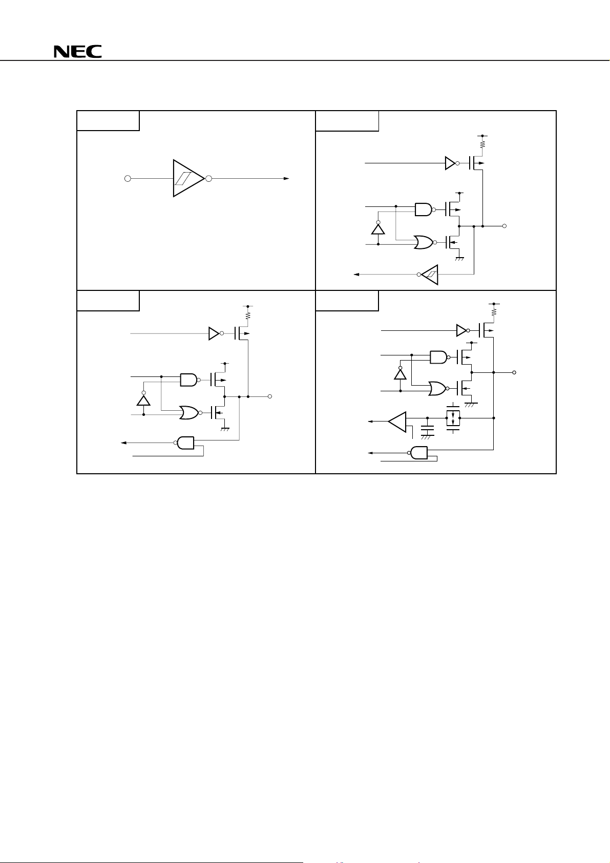
Figure 3-1. Pin Input/Output Circuits
µ
PD78081(A), 78082(A)
Type 2
IN
Schmitt-triggered input with hysteresis characteristic
V
Type 5-A
pullup
enable
V
data
output
disable
DD
P-ch
DD
P-ch
N-ch
input
enable
IN/OUT
Type 8-A
pullup
enable
data
output
disable
Type 11
pullup
enable
data
output
disable
Comparator
input
enable
P-ch
+
–
V
N-ch
REF
(threshold voltage)
V
DD
P-ch
N-ch
V
V
P-ch
N-ch
DD
P-ch
DD
V
IN/OUT
DD
P-ch
IN/OUT
13
Page 14
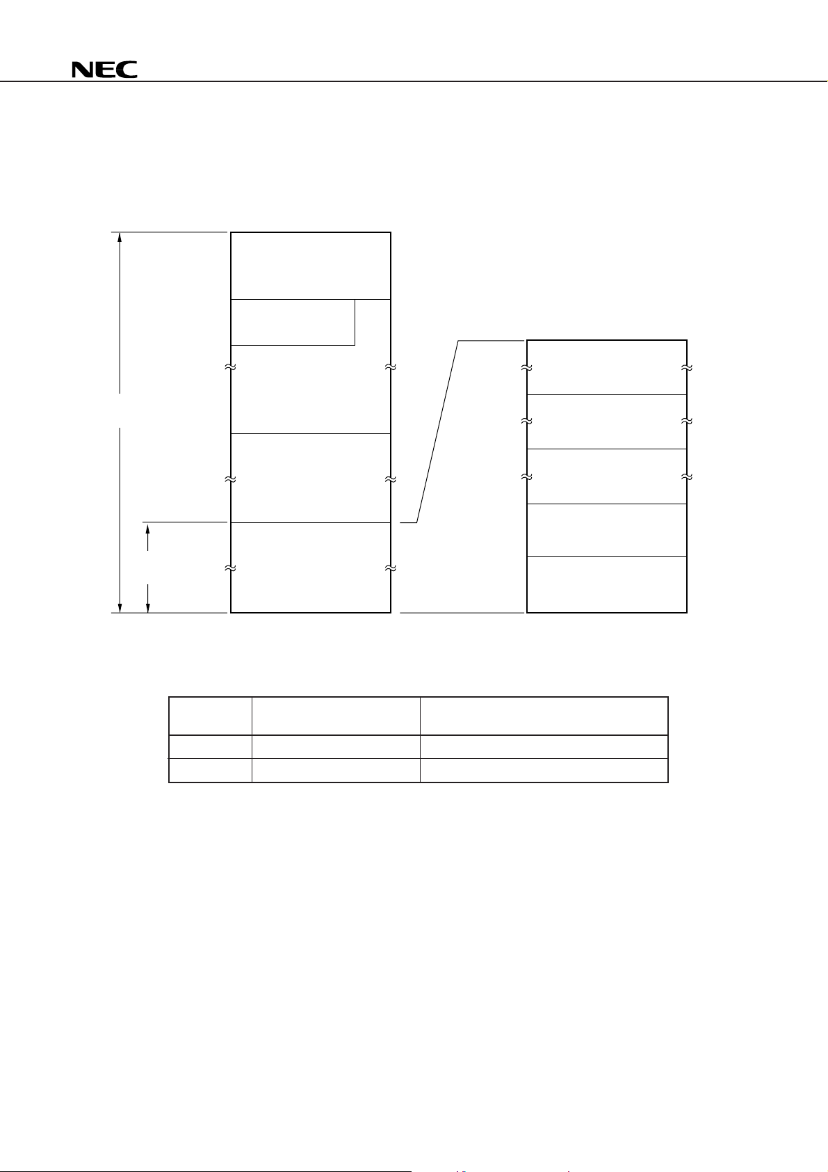
4. MEMORY SPACE
The memory map of the µPD78081(A) and 78082(A) is shown in Figure 4-1.
Figure 4-1. Memory Map
FFFFH
Special function registers
(SFR) 256 × 8 bits
FF00H
Data
memory
space
mmmmH – 1
Program
memory
space
FEFFH
FEE0H
FEDFH
mmmmH
nnnnH + 1
nnnnH
0000H
General-purpose registers
32 × 8 bits
Internal high-speed RAM
Use prohibited
Internal ROM
Note
Note
nnnnH
1000H
0FFFH
0800H
07FFH
0080H
007FH
0040H
003FH
0000H
µ
PD78081(A), 78082(A)
Program area
CALLF entry area
Program area
CALLT table area
Vector table area
Note The internal ROM and internal high-speed RAM capacities depend on the product (See the following table).
Part Number
µ
PD78081(A) 1FFFH FE00H
µ
PD78082(A) 3FFFH FD80H
Internal ROM Last Address Internal High-speed RAM Start Address
nnnnH mmmmH
14
Page 15
5. PERIPHERAL HARDWARE FUNCTIONS
5.1 Ports
Input/output ports are classified into two types.
• CMOS input (P00) : 1
• CMOS input/output (P01 to P03, Port 1, Port 3, Port 5, Port 7, Port 10) : 32
Total : 33
Table 5-1. Functions of Ports
Port Name Pin Name Function
Port 0 P00 Input only.
P01 to P03 Input/output port. Input/output can be specified bit-wise.
When used as an input port, on-chip pull-up resistor can be used by software.
Port 1 P10 to P17 Input/output port. Input/output can be specified bit-wise.
When used as an input port, on-chip pull-up resistor can be used by software.
Port 3 P30 to P37 Input/output port. Input/output can be specified bit-wise.
When used as an input port, on-chip pull-up resistor can be used by software.
Port 5 P50 to P57 Input/output port. Input/output can be specified bit-wise.
When used as an input port, on-chip pull-up resistor can be used by software.
LED can be driven directly up to 7 pins.
Port 7 P70 to P72 Input/output port. Input/output can be specified bit-wise.
When used as an input port, on-chip pull-up resistor can be used by software.
Port 10 P100, P101 Input/output port. Input/output can be specified bit-wise.
When used as an input port, on-chip pull-up resistor can be used by software.
µ
PD78081(A), 78082(A)
15
Page 16
5.2 Clock Generator
Main system clock generator is incorporated.
It is possible to change the minimum instruction execution time.
µ
• 0.4
s/0.8 µs/1.6 µs/3.2 µs/6.4 µs/12.8 µs (at main system clock frequency of 5.0 MHz)
Figure 5-1. Clock Generator Block Diagram
X1
X2
Main system
clock
oscillator
STOP
fX
Division
circuit
fXX
Selector
fX
2
Prescaler
f
XX
XX
f
2
2
2
µ
PD78081(A), 78082(A)
Prescaler
Clock to peripheral
XX
f
f
XX
3
4
2
2
Standby
control
circuit
Selector
hardware
CPU clock
(f
CPU)
5.3 Timer/Event Counter
There are the following three timer/event counter channels:
• 8-bit timer/event counter : 2 channels
• Watchdog timer : 1 channel
Table 5-2. Types and Functions of Timer/Event Counters
8-bit Timer/Event Counter 5, 6 Watchdog Timer
Type Interval timer 2 channels 1 channel
External event counter 2 channels —
Function Timer output 2 outputs —
PWM output 2 outputs —
Square wave output 2 outputs —
Interrupt request 2 1
16
Page 17
µ
f
XX
f
XX
5
f
XX
6
f
XX
7
2
f
XX
8
2
f
XX
9
2
f
XX
11
2
INTWDT
maskable
interrupt request
RESET
INTWDT
non-maskable
interrupt request
Prescaler
Selector
Control
circuit
4
22 2
8-bit counter
f
XX
3
2
PD78081(A), 78082(A)
Figure 5-2. 8-Bit Timer/Event Counter 5, 6 Block Diagram
Internal bus
8-bit compare register
(CRn0)
2fXX to fXX/2
fXX/2
TI5/P100/TO5,
TI6/P101/TO6
n = 5, 6
Match
9
11
8-bit timer register n
(TMn)
OVF
Output control
circuit
INTTMn
TO5/P100/TI5,
TO6/P101/TI6
Selector
Clear
Internal bus
Figure 5-3. Watchdog Timer Block Diagram
17
Page 18
µ
PD78081(A), 78082(A)
5.4 Clock Output Control Circuit
This circuit can output clocks of the following frequencies:
• 19.5 kHz/39.1 kHz/78.1 kHz/156 kHz/313 kHz/625 kHz/1.25 MHz/2.5 MHz/5.0 MHz (at main system clock
frequency of 5.0 MHz)
Figure 5-4. Clock Output Control Circuit Block Diagram
fXX
fXX/2
2
f
XX/2
3
fXX/2
fXX/2
fXX/2
fXX/2
fXX/2
4
5
6
7
Selector
Synchronization
circuit
Output control
circuit
PCL/P35
5.5 Buzzer Output Control Circuit
This circuit can output clocks of the following frequencies that can be used for driving buzzers:
• 1.2 kHz/2.4 kHz/4.9 kHz/9.8 kHz (at main system clock frequency of 5.0 MHz)
f
XX/2
fXX/2
fXX/2
Figure 5-5. Buzzer Output Control Circuit Block Diagram
9
10
11
Selector
Output control
circuit
BUZ/P36
18
Page 19

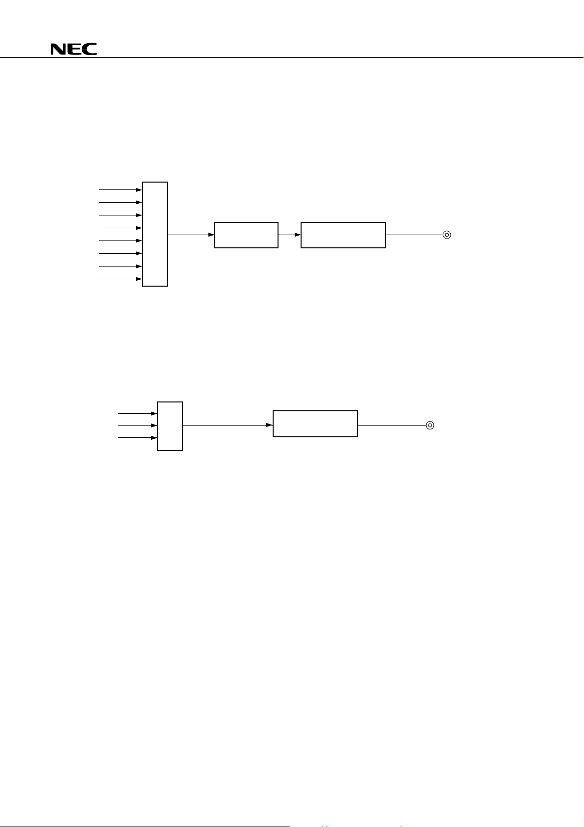
5.6 A/D Converter
The A/D converter consists of eight 8-bit resolution channels.
A/D conversion can be started by the following two methods:
• Hardware starting
• Software starting
Figure 5-6. A/D Converter Block Diagram
ANI0/P10
ANI1/P11
ANI2/P12
ANI3/P13
ANI4/P14
ANI5/P15
ANI6/P16
ANI7/P17
Sample & hold circuit
Selector
Successive approximation
register (SAR)
Voltage comparator
µ
PD78081(A), 78082(A)
Series resistor string
DD
AV
REF
AV
Tap selector
SS
AV
INTP3/P03
Edge
detector
Control
circuit
A/D conversion result
register (ADCR)
Internal bus
INTAD
INTP3
19
Page 20

µ
5.7 Serial Interface
There is one on-chip serial interface channel synchronous with the clock.
The serial interface channel 2 operates in the following two modes:
• 3-wire serial I/O mode : Starting bit MSB/LSB switching possible
• Asynchronous serial interface (UART) mode : On-chip dedicated baud rate generator
Figure 5-7. Serial Interface Channel 2 Block Diagram
Internal bus
PD78081(A), 78082(A)
XD/SI2/P70
R
TXD/SO2/P71
ASCK/SCK2/P72
Receive buffer
register (RXB/SIO2)
Direction control
circuit
Receive shift
register (RXS)
Receive control
circuit
Direction control
register (TXS/SIO2)
Transmit control
INTSER
INTSR/INTCSI2
Baud rate
generator
circuit
Transmit shift
circuit
SCK output
control circuit
XX to fXX/2
f
INTST
10
20
Page 21

6. INTERRUPT FUNCTIONS
Interrupt functions include three types and thirteen sources as shown below.
• Non-maskable : 1
• Maskable : 11
• Software : 1
Table 6-1. List of Interrupt Sources
µ
PD78081(A), 78082(A)
Interrupt Default Internal/
Type Priority External
Non- — INTWDT Overflow of watchdog timer (when the watchdog Internal 0004H (A)
maskable timer mode 1 is selected)
Maskable 0 INTWDT Overflow of watchdog timer (when the interval timer (B)
Software — BRK Execution of BRK instruction — 003EH (D)
Note 1
Name Trigger
mode is selected)
1 INTP1 Pin input edge detection External 0008H (C)
2 INTP2 000AH
3 INTP3 000CH
4 INTSER Occurrence of serial interface channel 2 UART Internal 0018H (B)
reception error
5 INTSR Completion of serial interface channel 2 UART 001AH
reception
INTCSI2 Completion of serial interface channel 2 3-wire
transfer
6 INTST Completion of serial interface channel 2 UART 001CH
transmission
7 INTAD Completion of A/D conversion 0028H
8 INTTM5 Generation of matching signal of 8-bit timer/event 002AH
counter 5
9 INTTM6 Generation of matching signal of 8-bit timer/event 002CH
counter 6
Interrupt Source
Vector
Table
Address Type
Basic
Configuration
Note 2
Notes 1. Default priority is the priority order when several maskable interrupt requests are generated at the same
time. 0 is the highest order and 9 is the lowest order.
2. Basic configuration types (A) to (D) correspond to (A) to (D) in Figure 6-1.
21
Page 22

Figure 6-1. Interrupt Function Basic Configuration (1/2)
(A) Internal non-maskable interrupt
Internal bus
µ
PD78081(A), 78082(A)
Interrupt
request
(B) Internal maskable interrupt
Interrupt
request
(C) External maskable interrupt
Priority
control
circuit
Internal bus
MK IE PR ISP
Priority
IF
control
circuit
Vector table
address
generator
Standby release
signal
Vector table
address
generator
Standby release
signal
22
Interrupt
request
External interrupt
mode register
(INTM0, INTM1)
Edge
detector
Internal bus
MK IE PR ISP
Priority control
IF
circuit
Vector table
address
generator
Standby
release
signal
Page 23

(D) Software interrupt
µ
PD78081(A), 78082(A)
Figure 6-1. Interrupt Function Basic Configuration (2/2)
Internal bus
Interrupt
request
IF : Interrupt request flag
IE : Interrupt enable flag
ISP : In-service priority flag
MK : Interrupt mask flag
PR : Priority specification flag
Priority
control
circuit
Vector table
address
generator
23
Page 24

µ
PD78081(A), 78082(A)
7. STANDBY FUNCTION
The standby function intends to reduce current consumption. It has the following two modes:
• HALT mode : In this mode, the CPU operation clock is stopped. The average current consumption can be
reduced by intermittent operation by combining this mode with the normal operation mode.
• STOP mode : In this mode, oscillation of the main system clock is stopped. All the operations performed
on the main system clock are suspended, and power consumption becomes extremely small.
Figure 7-1. Standby Function
Main system clock operation
STOP
Interrupt
request
STOP mode
(Oscillation of the main system
clock is stopped.)
instruction
Interrupt
8. RESET FUNCTION
There are the following two reset methods.
• External reset by RESET pin
• Internal reset by watchdog timer runaway time detection
HALT instruction
request
HALT mode
(Supply of clock to CPU is
stopped although clock
is generated.)
24
Page 25

µ
PD78081(A), 78082(A)
9. INSTRUCTION SET
(1) 8-bit instructions
MOV, XCH, ADD, ADDC, SUB, SUBC, AND, OR, XOR, CMP, MULU, DIVUW, INC, DEC, ROR, ROL, RORC,
ROLC, ROR4, ROL4, PUSH, POP, DBNZ
2nd Operand
#byte A r
1st Operand [HL + C]
A ADD MOV MOV MOV MOV MOV MOV MOV MOV ROR
ADDC XCH XCH XCH XCH XCH XCH XCH ROL
SUB ADD ADD ADD ADD ADD RORC
SUBC ADDC ADDC ADDC ADDC ADDC ROLC
AND SUB SUB SUB SUB SUB
OR SUBC SUBC SUBC SUBC SUBC
XOR AND AND AND AND AND
CMP OR OR OR OR OR
r MOV MOV INC
ADD DEC
ADDC
SUB
SUBC
AND
OR
XOR
CMP
B, C DBNZ
sfr MOV MOV
saddr MOV MOV DBNZ INC
ADD DEC
ADDC
SUB
SUBC
AND
OR
XOR
CMP
!addr16 MOV
PSW MOV MOV PUSH
[DE] MOV
Note
XOR XOR XOR XOR XOR
CMP CMP CMP CMP CMP
sfr saddr !addr16 PSW [DE] [HL]
[HL + byte]
[HL + B] $addr16
1 None
POP
Note Except r = A
25
Page 26

µ
PD78081(A), 78082(A)
2nd Operand
#byte A r sfr saddr !addr16 PSW [DE] [HL]
1st Operand [HL + C]
[HL] MOV ROR4
[HL + byte] MOV
[HL + B]
[HL + C]
X MULU
C
[HL + byte]
[HL + B] $addr16
1 None
ROL4
DIVUW
(2) 16-bit instructions
MOVW, XCHW, ADDW, SUBW, CMPW, PUSH, POP, INCW, DECW
2nd Operand
1st Operand
AX ADDW MOVW MOVW MOVW MOVW MOVW
rp MOVW MOVW
sfrp MOVW MOVW
saddrp MOVW MOVW
!addr16 MOVW
SP MOVW MOVW
#word AX rp
SUBW XCHW
CMPW
Note
Note
sfrp saddrp !addr16 SP None
INCW
DECW
PUSH
POP
Note Only when rp = BC, DE, HL
26
Page 27

(3) Bit manipulation instructions
MOV1, AND1, OR1, XOR1, SET1, CLR1, NOT1, BT, BF, BTCLR
µ
PD78081(A), 78082(A)
2nd Operand
1st Operand
A.bit MOV1 BT SET1
sfr.bit MOV1 BT SET1
saddr.bit MOV1 BT SET1
PSW.bit MOV1 BT SET1
[HL].bit MOV1 BT SET1
CY MOV1 MOV1 MOV1 MOV1 MOV1 SET1
A.bit sfr.bit saddr.bit PSW.bit [HL].bit CY $addr16 None
BF CLR1
BTCLR
BF CLR1
BTCLR
BF CLR1
BTCLR
BF CLR1
BTCLR
BF CLR1
BTCLR
AND1 AND1 AND1 AND1 AND1 CLR1
OR1 OR1 OR1 OR1 OR1 NOT1
XOR1 XOR1 XOR1 XOR1 XOR1
(4) Call instructions/Branch instructions
CALL, CALLF, CALLT, BR, BC, BNC, BZ, BNZ, BT, BF, BTCLR, DBNZ
2nd Operand
AX !addr16 !addr11 [addr5] $addr16
1st Operand
Basic instruction BR CALL CALLF CALLT BR
BR BC
Compound instruction BT
(5) Other instructions
ADJBA, ADJBS, BRK, RET, RETI, RETB, SEL, NOP, EI, DI, HALT, STOP
BNC
BZ
BNZ
BF
BTCLR
DBNZ
27
Page 28

10. ELECTRICAL SPECIFICATIONS
• Electrical specifications of µPD78081(A) and 78082(A) (1/11)
µ
PD78081(A), 78082(A)
Absolute Maximum Ratings (T
Parameter Symbol Test Conditions Ratings Unit
Supply voltage V
Input voltage V
Output voltage V
Analog input voltage V
Output current, high I
Output current, low I
Operating ambient temperature T
Storage temperature T
A = 25°C)
DD –0.3 to +7.0 V
AV
DD –0.3 to VDD + 0.3 V
AV
REF –0.3 to VDD + 0.3 V
AV
SS –0.3 to +0.3 V
I –0.3 to VDD + 0.3 V
O –0.3 to VDD + 0.3 V
AN P10 to P17 Analog input pins
OH Per pin –10 mA
AVSS – 0.3 to AVREF + 0.3
Total of P10 to P17, P50 to P54, P70 to P72, –15 mA
P100, P101
Total of P01 to P03, P30 to P37, P55 to P57 –15 mA
Note
OL
Per pin Peak value 30 mA
r.m.s. value 15 mA
Total of P50 to P54 Peak value 100 mA
r.m.s. value 70 mA
Total of P55 to P57 Peak value 100 mA
r.m.s. value 70 mA
Total of P10 to P17, P70 to P72, Peak value 50 mA
P100, P101
r.m.s. value 20 mA
Total of P01 to P03, P30 to P37 Peak value 50 mA
r.m.s. value 20 mA
A –40 to +85 °C
stg –65 to +150 °C
V
Note The r.m.s. value should be calculated as follows: [r.m.s. value] = [Peak value] × Duty
Caution If the absolute maximum rating of even one of the above parameters is exceeded, the quality of the
product may be degraded. The absolute maximum ratings are therefore the rated values that may,
if exceeded, physically damage the product. Be sure to use the product with all the absolute
maximum ratings observed.
Capacitance (T
Parameter Symbol Test Conditions MIN. TYP. MAX. Unit
Input capacitance CIN f = 1 MHz, Unmeasured pins returned to 0 V. 15 pF
I/O capacitance C
A = 25°C, VDD = VSS = 0 V)
IO f = 1 MHz, P01 to P03, P10 to P17, P30 to 15 pF
Unmeasured pins P37, P50 to P57, P70 to P72,
returned to 0 V. P100, P101
Remark Unless otherwise specified, alternate-function pin characteristics are the same as port pin characteristics.
28
Page 29

• Electrical specifications of µPD78081(A) and 78082(A) (2/11)
µ
PD78081(A), 78082(A)
Main System Clock Oscillator Characteristics (T
Resonator
Ceramic Oscillation frequency V
resonator (fX)
Crystal Oscillation frequency 1.0 5.0 MHz
resonator (fX)
External clock X1 input frequency 1.0 5.0 MHz
Recommended
Circuit
IC
X1
X2
C2
C1
IC
X1
X2
C2
C1
X2 X1
PD74HCU04
µ
Parameter
Note 1
Oscillation stabilization After V
Note 2
time
Note 1
Oscillation stabilization VDD = 4.5 to 5.5 V 10 ms
Note 2
time
Note 1
(fX)
X1 input high-/low-level 85 500 ns
widths (t
XH, tXL)
A = –40 to +85°C, V DD = 1.8 to 5.5 V)
Test Conditions
DD = Oscillation voltage 1.0 5.0 MHz
MIN.
TYP.
range
DD came to MIN. 4 ms
of oscillation voltage range
MAX.
30
Unit
Notes 1. Only the oscillator characteristics are shown. For the instruction execution time, refer to AC Characteristics.
2. Time required for oscillation to stabilize after a reset or the STOP mode has been released.
Caution When using the oscillation circuit of the main system clock, wire the portion enclosed in broken lines
in the figures as follows to avoid adverse influence on the wiring capacitance:
• Keep the wiring length as short as possible.
• Do not cross the wiring over other signal lines.
• Do not route the wiring in the vicinity of lines through which a high fluctuating current flows.
• Always keep the ground point of the capacitor of the oscillation circuit at the same potential as
SS.
V
• Do not connect the ground pattern through which a high current flows.
• Do not extract signals from the oscillation circuit.
29
Page 30

• Electrical specifications of µPD78081(A) and 78082(A) (3/11)
µ
PD78081(A), 78082(A)
DC Characteristics (T
A = –40 to +85°C, VDD = 1.8 to 5.5 V)
Parameter Symbol Test Conditions MIN. TYP. MAX. Unit
Input voltage, high V
Input voltage, low V
Output voltage, high V
Output voltage, low V
Input leak current, high I
Input leak current, low I
Output leak current, high I
Output leak current, low I
IH1 P10 to P17, P30 to VDD = 2.7 to 5.5 V 0.7 VDD VDD V
V
IH2 P00 to P03, P33, P34, VDD = 2.7 to 5.5 V 0.8 VDD VDD V
V
IH3 X1, X2 VDD = 2.7 to 5.5 V VDD – 0.5 VDD V
IL1 P10 to P17, P30 to VDD = 2.7 to 5.5 V 0 0.3 VDD V
V
IL2 P00 to P03, P33, P34, VDD = 2.7 to 5.5 V 0 0.2 VDD V
V
IL3 X1, X2 VDD = 2.7 to 5.5 V 0 0.4 V
OH VDD = 4.5 to 5.5 V, IOH = –1 mA VDD – 1.0 V
OL P50 to P57 VDD = 2.0 to 4.5 V, 0.8 V
LIH1 VIN = VDD
I
LIH2 X1, X2 20
LIL1 VIN = 0 V
I
LIL2 X1, X2 –20
LOH VOUT = VDD 3
LOL VOUT = 0 V –3
Software pull-up resistance R V
P32, P35 to P37, P50
to P57, P71
P70, P72, P100, P101,
RESET
P32, P35 to P37, P50
to P57, P71
P70, P72, P100,
P101, RESET
I
OH = –100
µ
AVDD – 0.5 V
P01 to P03, P10 to V
P17, P30 to P37, P70 I
to P72, P100, P101 I
IN = 0 V
0.8 VDD
0.85 VDD
V
DD – 0.2 VDD V
0
0
VDD
VDD
0.2 VDD
0.15 V
DD
0 0.2 V
I
OL = 10 mA
V
DD = 4.5 to 5.5 V, 0.4 2.0 V
I
OL = 15 mA
DD = 4.5 to 5.5 V, 0.4 V
OL = 1.6 mA
OL = 400
P00 to P03, P10 to P17,
µ
A 0.5 V
3
P30 to P37, P50 to P57,
P70 to P72, P100,
P101, RESET
P00 to P03, P10 to P17,
–3
P30 to P37, P50 to P57,
P70 to P72, P100,
P101, RESET
P01 to P03, P10 to P17,
15 40 90 kΩ
P30 to P37, P50 to P57,
P70 to P72, P100,
P101
V
V
V
V
µ
A
µ
A
µ
A
µ
A
µ
A
µ
A
Remark Unless otherwise specified, alternate-function pin characteristics are the same as port pin characteristics.
30
Page 31

• Electrical specifications of µPD78081(A) and 78082(A) (4/11)
µ
PD78081(A), 78082(A)
DC Characteristics (T
A = –40 to +85°C, VDD = 1.8 to 5.5 V)
Parameter Symbol Test Conditions MIN. TYP. MAX. Unit
Supply current
Note 1
IDD1 5.0-MHz crystal oscil- VDD = 5.0 V ±10%
lation operating mode V
(f
XX = 2.5 MHz)
Note 2
5.0-MHz crystal oscil- V
lation operating mode V
(f
XX = 5.0 MHz)
Note 3
DD = 3.0 V ±10%
VDD = 2.0 V ±10%
DD = 5.0 V ±10%
DD = 3.0 V ±10%
Note 4
Note 5
Note 5
Note 4
Note 5
4.5 13.5 mA
0.7 2.1 mA
0.4 1.2 mA
8.0 24.0 mA
0.9 2.7 mA
IDD2 5.0-MHz crystal oscil- VDD = 5.0 V ±10% 1.4 4.2 mA
lation HALT mode V
(f
XX = 2.5 MHz)
Note 2
5.0-MHz crystal oscil- V
lation HALT mode V
(f
XX = 5.0 MHz)
Note 3
IDD3 STOP mode VDD = 5.0 V ±10% 0.1 30
DD = 3.0 V ±10% 0.5 1.5 mA
VDD = 2.0 V ±10% 280 840
DD = 5.0 V ±10% 1.6 4.8 mA
DD = 3.0 V ±10% 0.65 1.95 mA
V
DD = 3.0 V ±10% 0.05 10
V
DD = 2.0 V ±10% 0.05 10
µ
A
µ
A
µ
A
µ
A
Notes 1. Not including AVREF and AVDD currents or port currents (including current flowing into on-chip pull-up
resistors).
XX = fX/2 operation (when oscillation mode selection register (OSMS) is set to 00H).
2. f
XX = fX operation (when oscillation mode selection register (OSMS) is set to 01H).
3. f
4. High-speed mode operation (when processor clock control register (PCC) is set to 00H).
5. Low-speed mode operation (when processor clock control register (PCC) is set to 04H).
Remark f
XX : Main system clock frequency (fX or fX/2)
X : Main system clock oscillation frequency
f
31
Page 32

• Electrical specifications of µPD78081(A) and 78082(A) (5/11)
y
y
AC Characteristics
µ
PD78081(A), 78082(A)
(1) Basic Operation (T
A = –40 to +85°C, VDD = 1.8 to 5.5 V)
Parameter Symbol Test Conditions MIN. TYP. MAX. Unit
Cycle time T
CY fXX = fX/2
Note 1
VDD = 2.7 to 5.5 V 0.8 64
(minimum instruction execution 2. 0 6 4
time) f
TI5, TI6 f
TI VDD = 4.5 to 5.5 V 0 4 MHz
XX = fX
Note 2
3.5 V ≤ VDD ≤ 5.5 V
2.7 V ≤ VDD < 3.5 V
0.4 32
0.8 32
input frequency 0 275 kHz
TI5, TI6 input high-/ t
low-level widths t
Interrupt request input high-/ t
low-level widths t
RESET low-level width t
TIH,VDD = 4.5 to 5.5 V 100 ns
TIL 1.8
INTH,VDD = 2.7 to 5.5 V 10
INTL 20
RSL VDD = 2.7 to 5.5 V 10
20
Notes 1. When oscillation mode selection register (OSMS) is set to 00H.
2. When OSMS is set to 01H.
Remark f
XX : Main system clock frequency (f X or fX/2)
X : Main system clock oscillation frequency
f
µ
s
µ
s
µ
s
µ
s
µ
s
µ
s
µ
s
µ
s
µ
s
CY vs VDD TCY vs VDD
T
(Main System Clock fXX = fX/2 Operation) (Main System Clock fXX = fX Operation)
µ
2.0
1.0
Cycle Time T CY [ s]
0.5
0.4
60
10
Operation
Guaranteed
Range
0
123456
Power Suppl
Voltage VDD [V]
µ
2.0
1.0
Cycle Time T CY [ s]
0.5
0.4
60
10
Operation
Guaranteed
Range
0
123456
Power Suppl
Voltage VDD [V]
32
Page 33

• Electrical specifications of µPD78081(A) and 78082(A) (6/11)
µ
PD78081(A), 78082(A)
(2) Serial Interface (T
A = –40 to +85°C, VDD = 1.8 to 5.5 V)
(a) 3-wire serial I/O mode (SCK2... Internal clock output)
Parameter Symbol Conditions MIN. TYP. MAX. Unit
SCK2 cycle time tKCY1 4.5 V ≤ VDD ≤ 5.5 V 800 ns
2.7 V ≤ VDD < 4.5 V 1,600 ns
2.0 V ≤ VDD < 2.7 V 3,200 ns
4,800 ns
SCK2 high-/low-level tKH1, tKL1 VDD = 4.5 to 5.5 V tKCY1 /2 – 50 ns
widths tKCY1/2 – 100 ns
SI2 setup time tSIK1 4.5 V ≤ VDD ≤ 5.5 V 100 ns
(to SCK2↑) 2.7 V ≤ VDD < 4.5 V 150 ns
2.0 V ≤ VDD < 2.7 V 300 ns
400 ns
SI2 hold time t
(from SCK2↑)
SO2 output delay time tKSO1 C = 100 pF
from SCK2↓
KSI1 400 ns
Note
300 ns
Note C is the load capacitance of SCK2 and SO2 output lines.
(b) 3-wire serial I/O mode (SCK2... External clock input)
Parameter Symbol Conditions MIN. TYP. MAX. Unit
SCK2 cycle time tKCY2 4.5 V ≤ VDD ≤ 5.5 V 800 ns
2.7 V ≤ VDD < 4.5 V 1,600 ns
2.0 V ≤ VDD < 2.7 V 3,200 ns
4,800 ns
SCK2 high-/low-level tKH2, tKL2 4.5 V ≤ VDD ≤ 5.5 V 400 ns
widths 2.7 V ≤ VDD < 4.5 V 800 ns
2.0 V ≤ VDD < 2.7 V 1,600 ns
2,400 ns
SI2 setup time tSIK2 VDD = 2.0 to 5.5 V 100 ns
(to SCK2↑) 150 ns
SI2 hold time tKSI2 400 ns
(from SCK2↑)
SO2 output delay time tKSO2 C = 100 pF
from SCK2↓ 500 ns
SCK2 rise/fall time tR2, tF2 1,000 ns
Note
VDD = 2.0 to 5.5 V 300 ns
Note C is the load capacitance of SO2 output line.
33
Page 34

µ
PD78081(A), 78082(A)
• Electrical specifications of µPD78081(A) and 78082(A) (7/11)
(c) UART mode (Dedicated baud rate generator output)
Parameter Symbol Conditions MIN. TYP. MAX. Unit
Transfer rate 4.5 V ≤ VDD ≤ 5.5 V 78,125 bps
2.7 V ≤ VDD < 4.5 V 39,063 bps
2.0 V ≤ VDD < 2.7 V 19,531 bps
9,766 bps
(d) UART mode (External clock input)
Parameter Symbol Conditions MIN. TYP. MAX. Unit
ASCK cycle time tKCY3 4.5 V ≤ VDD ≤ 5.5 V 800 ns
2.7 V ≤ VDD < 4.5 V 1,600 ns
2.0 V ≤ VDD < 2.7 V 3,200 ns
4,800 ns
ASCK high-/low-level t KH3, tKL3 4.5 V ≤ VDD ≤ 5.5 V 400 ns
widths 2.7 V ≤ VDD < 4.5 V 800 ns
2.0 V ≤ VDD < 2.7 V 1,600 ns
2,400 ns
Transfer rate 4.5 V ≤ VDD ≤ 5.5 V 39,063 bps
2.7 V ≤ VDD < 4.5 V 19,531 bps
2.0 V ≤ VDD < 2.7 V 9,766 bps
6,510 bps
ASCK rise/fall time tR3, tF3 1,000 ns
34
Page 35

• Electrical specifications of µPD78081(A) and 78082(A) (8/11)
0.8 V
DD
0.2 V
DD
0.8 V
DD
0.2 V
DD
Test points
AC Timing Test Points (excluding X1 Input)
Clock Timing
1/fX
tXL tXH
µ
PD78081(A), 78082(A)
TI Timing
X1 Input
TI5, TI6
VIH3 (MIN.)
VIL3 (MAX.)
1/fTI
tTIHtTIL
35
Page 36

• Electrical specifications of µPD78081(A) and 78082(A) (9/11)
Serial Transfer Timing
3-wire serial I/O mode :
tKCY1, 2
tKL1, 2 tKH1, 2
tR2
SCK2
tSIK1, 2 tKSI1, 2
µ
PD78081(A), 78082(A)
tF2
SI2
tKSO1, 2
SO2
Input data
Output data
UART mode (external clock input) :
KCY3
t
ASCK
KL3
t
tR3
t
KH3
tF3
A/D Converter Characteristics (TA = –40 to +85°C, AVDD = VDD = 1.8 to 5.5 V, AVSS = VSS = 0 V)
Parameter Symbol Conditions MIN. TYP. MAX. Unit
Resolution
Overall error
Conversion time
Sampling time
Analog input voltage
Reference voltage
Resistance between AVREF and AVSS
Note
2.7 V ≤ AVREF ≤ AVDD 0.6 %
1.8 V ≤ AVREF < 2.7 V 1.4 %
tCONV 2.0 V ≤ AVDD ≤ 5.5 V 19.1 200
1.8 V ≤ AVDD < 2.0 V 38.2 200
tSAMP 12/fxx
VIAN AVSS AVREF V
AVREF 1.8 AVDD V
RAIREF 4 14 kΩ
8 8 8 bit
Note Overall error excluding quantization error (±1/2LSB). It is indicated as a ratio to the full-scale value.
Remark f
XX : Main system clock frequency (fX or fX/2)
X : Main system clock oscillation frequency
f
36
µ
s
µ
s
µ
s
Page 37

• Electrical specifications of µPD78081(A) and 78082(A) (10/11)
t
SREL
t
WAIT
V
DD
RESET
STOP instruction execution
STOP mode
Data retention mode
Internal reset operation
HALT mode
Operating mode
V
DDDR
t
SREL
t
WAIT
V
DD
STOP instruction execution
STOP mode
Data retention mode
HALT mode
Operating mode
Standby release signal
(interrupt request)
V
DDDR
µ
PD78081(A), 78082(A)
Data Memory STOP Mode Low Supply Voltage Data Retention Characteristics (T
A = –40 to +85°C)
Parameter Symbol Conditions MIN. TYP. MAX. Unit
Data retention power VDDDR 1.8 5.5 V
supply voltage
Data retention power IDDDR VDDDR = 1.8 V 0.1 10
µ
A
supply current
Release signal set time
tSREL 0
µ
s
Oscillation stabilization tWAIT Release by RESET 217/fx ms
wait time
Release by interrupt request Note ms
Note In combination with bits 0 to 2 (OSTS0 to OSTS2) of oscillation stabilization time select register (OSTS),
12
selection of 2
Remark f
XX : Main system clock frequency (fX or fX/2)
X : Main system clock oscillation frequency
f
/fXX and 214/fXX to 217/fXX is possible.
Data Retention Timing (STOP mode release by RESET)
Data Retention Timing (Standby release signal: STOP mode release by interrupt request signal)
37
Page 38

• Electrical specifications of µPD78081(A) and 78082(A) (11/11)
Interrupt Request Input Timing
tINTL tINTH
INTP1 to INTP3
RESET Input Timing
tRSL
RESET
µ
PD78081(A), 78082(A)
38
Page 39

• Electrical specifications of µPD78081(A2) (1/10)
µ
PD78081(A), 78082(A)
Absolute Maximum Ratings (T
Parameter Symbol Test Conditions Ratings Unit
Supply voltage V
Input voltage V
Output voltage V
Analog input voltage V
Output current, high I
Output current, low I
Operating ambient temperature T
Storage temperature T
A = 25°C)
DD –0.3 to +7.0 V
AV
DD –0.3 to VDD + 0.3 V
AV
REF –0.3 to VDD + 0.3 V
AV
SS –0.3 to +0.3 V
I –0.3 to VDD + 0.3 V
O –0.3 to VDD + 0.3 V
AN P10 to P17 Analog input pins
OH Per pin –10 mA
AVSS – 0.3 to AVREF + 0.3
Total of P10 to P17, P50 to P54, P70 to P72, –15 mA
P100, P101
Total of P01 to P03, P30 to P37, P55 to P57 –15 mA
Note
OL
Per pin Peak value 30 mA
r.m.s. value 15 mA
Total of P50 to P54 Peak value 100 mA
r.m.s. value 70 mA
Total of P55 to P57 Peak value 100 mA
r.m.s. value 70 mA
Total of P10 to P17, P70 to P72, Peak value 50 mA
P100, P101
r.m.s. value 20 mA
Total of P01 to P03, P30 to P37 Peak value 50 mA
r.m.s. value 20 mA
A –40 to +125 °C
stg –65 to +150 °C
V
Note The r.m.s. value should be calculated as follows: [r.m.s. value] = [Peak value] × Duty
Caution If the absolute maximum rating of even one of the above parameters is exceeded, the quality of the
product may be degraded. The absolute maximum ratings are therefore the rated values that may,
if exceeded, physically damage the product. Be sure to use the product with all the absolute
maximum ratings observed.
Permissible Pin Sink Current Characteristics with Overvoltage Applied
Pending
Capacitance (T
Parameter Symbol Test Conditions MIN. TYP. MAX. Unit
Input capacitance CIN f = 1 MHz, Unmeasured pins returned to 0 V. 15 pF
I/O capacitance C
A = 25°C, VDD = V SS = 0 V)
IO f = 1 MHz, P01 to P03, P10 to P17, P30 to 15 pF
Unmeasured pins P37, P50 to P57, P70 to P72,
returned to 0 V. P100, P101
Remark Unless otherwise specified, alternate-function pin characteristics are the same as port pin characteristics.
39
Page 40

• Electrical specifications of µPD78081(A2) (2/10)
µ
PD78081(A), 78082(A)
Main System Clock Oscillator Characteristics (T
Resonator
Crystal Oscillation frequency 1.0 7.0 MHz
resonator (fX)
External clock X1 input frequency 1.0 7.0 MHz
Recommended
Circuit
IC
PD74HCU04
µ
X2
C2
C1
X2 X1
X1
Parameter
Note 1
Oscillation stabilization 10 ms
Note 2
time
Note 1
(fX)
X1 input high-/low-level 64 500 ns
widths (t
XH, tXL)
A = –40 to +125°C, VDD = 5 V ±10%)
Test Conditions
MIN.
TYP.
MAX.
Unit
Notes 1. Only the oscillator characteristics are shown. For the instruction execution time, refer to AC Characteristics.
2. Time required for oscillation to stabilize after a reset or the STOP mode has been released.
Caution When using the oscillation circuit of the main system clock, wire the portion enclosed in broken lines
in the figure as follows to avoid adverse influence on the wiring capacitance:
• Keep the wiring length as short as possible.
• Do not cross the wiring over other signal lines.
• Do not route the wiring in the vicinity of lines through which a high fluctuating current flows.
• Always keep the ground point of the capacitor of the oscillation circuit at the same potential as
SS.
V
• Do not connect the ground pattern through which a high current flows.
• Do not extract signals from the oscillation circuit.
40
Page 41

• Electrical specifications of µPD78081(A2) (3/10)
DC Characteristics (TA = –40 to +125°C, VDD = 5 V ±10%)
Parameter Symbol Test Conditions MIN. TYP. MAX. Unit
Input voltage, high V
Input voltage, low V
Output voltage, high V
Output voltage, low V
Input leak current, high I
Input leak current, low I
Output leak current, high I
Output leak current, low I
Software pull-up resistance R V
Supply current
Note 1
IH1 P10 to P17, P30 to P32, P35 to P37, P50 to 0.7 VDD VDD V
P57
V
IH2 P00 to P03, P33, P34, P70 to P72, P100, 0.9 VDD VDD V
P101, RESET
V
IH3 X1, X2 VDD – 0.2 VDD V
IL1 P10 to P17, P30 to P32, P35 to P37, P50 to 0 0.3 VDD V
P57
V
IL2 P00 to P03, P33, P34, P70 to P72, P100, 0 0.16 VDD V
P101, RESET
V
IL3 X1, X2 0 0.4 V
OH IOH = –1 mA VDD – 1.0 V
I
OH = –100
OL P50 to P57 IOL = 15 mA 0.4 2.2 V
µ
AVDD – 0.5 V
P01 to P03, P10 to I
P17, P30 to P37, P70 I
to P72, P100, P101
LIH1 VIN = VDD
I
LIH2 X1, X2 20
LIL1 VIN = 0 V
I
LIL2 X1, X2 –20
LOH VOUT = VDD 10
LOL VOUT = 0 V –10
IN = 0 V
IDD1 7.0-MHz crystal oscillation operating mode 9.0 29.0 mA
(f
XX = 3.5 MHz)
Notes 2, 3
5.0-MHz crystal oscillation operating mode 5.5 16.5 mA
(f
XX = 2.5 MHz)
Notes 2, 3
IDD2 7.0-MHz crystal oscillation HALT mode 1.5 7.2 mA
(f
XX = 3.5 MHz)
Note 2
5.0-MHz crystal oscillation HALT mode 1.2 6.5 mA
(f
XX = 2.5 MHz)
Note 2
IDD3 STOP mode 0.1 1,000
µ
PD78081(A), 78082(A)
OL = 1.6 mA 0.45 V
OL = 400
P00 to P03, P10 to P17,
µ
A 0.5 V
10 V
P30 to P37, P50 to P57,
P70 to P72, P100,
P101, RESET
P00 to P03, P10 to P17,
–10
P30 to P37, P50 to P57,
P70 to P72, P100,
P101, RESET
P01 to P03, P10 to P17,
15 40 120 kΩ
P30 to P37, P50 to P57,
P70 to P72, P100,
P101
µ
A
µ
A
µ
A
µ
A
µ
A
µ
A
Notes 1.
Not including AV
REF
and AVDD currents or port currents (including current flowing into on-chip pull-up resistors).
2. fXX = fX/2 operation (when oscillation mode selection register (OSMS) is set to 00H).
3. High-speed mode operation (when processor clock control register (PCC) is set to 00H).
Remarks 1. f
XX : Main system clock frequency (fX or fX/2)
X : Main system clock oscillation frequency
2. f
3. Unless otherwise specified, alternate-function pin characteristics are the same as port pin characteristics.
41
Page 42

• Electrical specifications of µPD78081(A2) (4/10)
y
]
AC Characteristics
µ
PD78081(A), 78082(A)
(1) Basic Operation (T
A = –40 to +125°C, VDD = 5 V ±10%)
Parameter Symbol Test Conditions MIN. TYP. MAX. Unit
Cycle time (minimum T
CY fXX = fX/2
Note
instruction execution time)
TI5, TI6 input frequency f
TI5, TI6 input high-/ t
TI 0 2 kHz
TIH, tTIL 200 ns
low-level widths
Interrupt request input high-/ t
INTH, tINTL 10
low-level widths
RESET low-level width t
RSL 10
Note When oscillation mode selection register (OSMS) is set to 00H.
Remark f
XX : Main system clock frequency (f X or fX/2)
X : Main system clock oscillation frequency
f
T
CY vs VDD
(Main System Clock fXX = fX/2 Operation)
0.57 32
µ
s
µ
s
µ
s
µ
2.0
1.0
Cycle Time T CY [ s]
0.5
60
10
0
123456
Power Suppl
Voltage VDD [V
Operation
Guaranteed Range
42
Page 43

• Electrical specifications of µPD78081(A2) (5/10)
µ
PD78081(A), 78082(A)
(2) Serial Interface (T
A = –40 to +125°C, VDD = 5 V ±10%)
(a) 3-wire serial I/O mode (SCK2... Internal clock output)
Parameter Symbol Conditions MIN. TYP. MAX. Unit
SCK2 cycle time tKCY1 1,000 ns
SCK2 high-/low-level t
widths
SI2 setup time tSIK1 150 ns
(to SCK2↑)
SI2 hold time tKSI1 500 ns
(from SCK2↑)
SO2 output delay time t
from SCK2↓
KH1, tKL1 tKCY1/2 – 100 ns
KSO1 C = 100 pF
Note
400 ns
Note C is the load capacitance of SCK2 and SO2 output lines.
(b) 3-wire serial I/O mode (SCK2... External clock input)
Parameter Symbol Conditions MIN. TYP. MAX. Unit
SCK2 cycle time tKCY2 1,000 ns
SCK2 high-/low-level tKH2, tKL2 500 ns
widths
SI2 setup time tSIK2 150 ns
(to SCK2↑)
SI2 hold time t
(from SCK2↑)
SO2 output delay time tKSO2 C = 100 pF
from SCK2↓
SCK2 rise/fall time t
KSI2 500 ns
Note
R2, tF2 1,000 ns
400 ns
Note C is the load capacitance of SO2 output line.
43
Page 44

µ
PD78081(A), 78082(A)
• Electrical specifications of µPD78081(A2) (6/10)
(c) UART mode (Dedicated baud rate generator output)
Parameter Symbol Conditions MIN. TYP. MAX. Unit
Transfer rate 76,923 bps
(d) UART mode (External clock input)
Parameter Symbol Conditions MIN. TYP. MAX. Unit
ASCK cycle time tKCY3 1,000 ns
ASCK high-/low-level t KH3, tKL3 500 ns
widths
Transfer rate 38,462 bps
ASCK rise/fall time tR3, tF3 1,000 ns
44
Page 45

• Electrical specifications of µPD78081(A2) (7/10)
AC Timing Test Points (excluding X1 Input)
0.8 V
DD
0.2 V
DD
Clock Timing
tXL tXH
Test points
1/fX
0.8 V
0.2 V
µ
PD78081(A), 78082(A)
DD
DD
TI Timing
X1 Input
TI5, TI6
VDD – 0.2 V
0.4 V
1/fTI
tTIHtTIL
45
Page 46

• Electrical specifications of µPD78081(A2) (8/10)
Serial Transfer Timing
3-wire serial I/O mode :
tKL1, 2 tKH1, 2
SCK2
tKCY1, 2
tR2
tSIK1, 2 tKSI1, 2
µ
PD78081(A), 78082(A)
tF2
SI2
tKSO1, 2
SO2
Input data
Output data
UART mode (external clock input) :
KCY3
t
ASCK
KL3
t
tR3
t
KH3
tF3
A/D Converter Characteristics (TA = –40 to +125°C, AVDD = VDD = 5 V ±10%, AVSS = VSS = 0 V)
Parameter Symbol Conditions MIN. TYP. MAX. Unit
Resolution
Overall error
Conversion time
Sampling time
Analog input voltage
Reference voltage
Resistance between AVREF and AVSS
Note
4.5 V ≤ AVREF ≤ AVDD 1.0 %
tCONV 23.8 100
tSAMP 12/fxx
VIAN AVSS AVREF V
AVREF 4.5 AVDD V
RAIREF 4 14 kΩ
8 8 8 bit
Note Overall error excluding quantization error (±1/2LSB). It is indicated as a ratio to the full-scale value.
Remark f
XX : Main system clock frequency (fX or fX/2)
X : Main system clock oscillation frequency
f
46
µ
s
µ
s
Page 47

• Electrical specifications of µPD78081(A2) (9/10)
tSREL
tWAIT
VDD
RESET
STOP instruction execution
STOP mode
Data retention mode
Internal reset operation
HALT mode
Operating mode
VDDDR
tSREL
tWAIT
VDD
STOP instruction execution
STOP mode
Data retention mode
HALT mode
Operating mode
Standby release signal
(interrupt request)
VDDDR
µ
PD78081(A), 78082(A)
Data Memory STOP Mode Low Supply Voltage Data Retention Characteristics (T
Parameter Symbol Conditions MIN. TYP. MAX. Unit
Data retention power V
supply voltage
Data retention power IDDDR VDDDR = 4.5 V 0.1 1,000
supply current
Release signal set time
Oscillation stabilization t
wait time
DDDR 4.5 5.5 V
tSREL 0
WAIT Release by RESET 2
Release by interrupt request Note ms
A = –40 to +125°C)
17
/fx ms
µ
A
µ
s
Note In combination with bits 0 to 2 (OSTS0 to OSTS2) of oscillation stabilization time select register (OSTS),
12
selection of 2
Remark f
XX : Main system clock frequency (fX or fX/2)
X : Main system clock oscillation frequency
f
/fXX and 214/fXX to 217/fXX is possible.
Data Retention Timing (STOP mode release by RESET)
Data Retention Timing (Standby release signal: STOP mode release by interrupt request signal)
47
Page 48

• Electrical specifications of µPD78081(A2) (10/10)
Interrupt Request Input Timing
tINTL tINTH
INTP1 to INTP3
RESET Input Timing
RESET
tRSL
µ
PD78081(A), 78082(A)
48
Page 49

11. PACKAGE DRAWINGS
44 PIN PLASTIC QFP ( 10)
NOTE
Each lead centerline is located within 0.15 mm (0.006 inch) of
its true position (T.P.) at maximum material condition.
P44GB-80-3B4-3
ITEM MILLIMETERS INCHES
A
B
C
13.6±0.4
10.0±0.2
10.0±0.2
0.535
0.394
0.394
D 13.6±0.4 0.535
F 1.0 0.039
G 1.0 0.039
H 0.35±0.10 0.014
I 0.15 0.006
J 0.8 (T.P.) 0.031 (T.P)
K 1.8±0.2 0.071
L 0.8±0.2 0.031
M 0.15 0.006
N 0.10 0.004
P 2.7 0.106
Q 0.1±0.1 0.004±0.004
R5°±5° 5°±5°
S 3.0 MAX. 0.119 MAX.
+0.017
–0.016
+0.008
–0.009
+0.008
–0.009
+0.017
–0.016
+0.004
–0.005
+0.008
–0.009
+0.009
–0.008
+0.004
–0.003
N
L
detail of lead end
G
M
I
J
H
A
F
M
Q
R
B
33
34
22
44
1
12
11
23
C D
S
P
K
+0.10
–0.05
µ
PD78081GB(A)-×××-3B4, 78082GB(A)-×××-3B4, 78081GB(A2)-×××-3B4
µ
PD78081(A), 78082(A)
Remark The shape and material of ES versions are the same as
those of mass-produced versions.
49
Page 50

µ
PD78081GB(A)-×××-3BS-MTX, 78082GB(A)-×××-3BS-MTX
44 PIN PLASTIC QFP ( 10)
A
B
µ
PD78081(A), 78082(A)
34
33
23
22
CD
44
1
11
12
F
J
G
H
M
I
K
P
N
NOTE
Each lead centerline is located within 0.16 mm (0.007 inch) of
its true position (T.P.) at maximum material condition.
L
detail of lead end
S
R
Q
M
ITEM MILLIMETERS INCHES
A 13.2±0.2 0.520
B 10.0±0.2
C 10.0±0.2
D 13.2±0.2
F
1.0
G
1.0
H
I
J
K
L 0.8±0.2
M 0.17 0.007
N
P
Q 0.125±0.075
R3° 3°
S 3.0 MAX.
+0.08
0.37
–0.07
0.16
0.8 (T.P.)
1.6±0.2
+0.06
–0.05
0.10
2.7
+7°
–3°
+0.008
–0.009
+0.008
0.394
–0.009
+0.008
0.394
–0.009
+0.008
0.520
–0.009
0.039
0.039
+0.003
0.015
–0.004
0.007
0.031 (T.P.)
0.063±0.008
+0.009
0.031
–0.008
+0.002
–0.003
0.004
0.106
0.005±0.003
+7°
–3°
0.119 MAX.
S44GB-80-3BS
50
Page 51

µ
PD78081(A), 78082(A)
12. RECOMMENDED SOLDERING CONDITIONS
µ
PD78081(A) and 78082(A) should be soldered and mounted under the conditions recommended in the table
below.
For detail of recommended soldering conditions, refer to the information document Semiconductor Device
Mounting Technology Manual (C10535E).
For soldering methods and conditions other than those recommended below, consult our sales representative.
Table 12-1. Surface Mounting Type Soldering Conditions
µ
PD78081GB(A)-×××-3B4 : 44-pin plastic QFP (10 × 10 mm)
µ
PD78082GB(A)-×××-3B4 : 44-pin plastic QFP (10 × 10 mm)
µ
PD78081GB(A2)-×××-3B4 : 44-pin plastic QFP (10 × 10 mm)
Soldering
Method
Infrared reflow
VPS
Wave soldering
Pin partial heating
Package peak temperature: 235°C, Reflow time: 30 seconds or below (at 210°C or
higher), Number of reflow processes: 3 max.
Package peak temperature: 215°C, Reflow time: 40 seconds or below (at 200°C or
higher), Number of reflow processes: 3 max.
Solder temperature: 260°C or below, Flow time: 10 seconds or below, Number of flow
processes: once, Preheating temperature: 120°C or below (package surface temperature)
Pin temperature: 300°C or below, Time: 3 seconds or below (per device side)
Soldering Conditions Symbol
IR35-00-3
VP15-00-3
WS60-00-1
—
Cautions 1. Use of more than one soldering method should be avoided (except for the pin partial heating
method).
µ
2. Because production of the
PD78081GB(A)-×××-3BS-MTX and 78082GB(A)-×××-3BS-MTX is still
in a planning stage, their soldering conditions are pending.
51
Page 52

µ
PD78081(A), 78082(A)
APPENDIX A. DEVELOPMENT TOOLS
The following development tools are available to support development of systems using the µPD78081(A) and
78082(A).
Language Processing Software
RA78K/0
CC78K/0
DF78083
CC78K/0-L
Notes 1, 2, 3, 4
Notes 1, 2, 3, 4
Notes 1, 2, 3, 4
Notes 1, 2, 3, 4
Assembler package common to the 78K/0 Series
C compiler package common to the 78K/0 Series
Device file used for the µPD78083 Subseries
C compiler library source file common to the 78K/0 Series
PROM Writing Tools
PG-1500 PROM programmer
PA-78P083GB Programmer adapter connected to the PG-1500
PG-1500 Controller
Notes 1, 2
Control program for the PG-1500
Debugging Tools
IE-78000-R In-circuit emulator common to the 78K/0 Series
IE-78000-R-A In-circuit emulator common to the 78K/0 Series (for integrated debugger)
IE-78000-R-BK Break board common to the 78K/0 Series
IE-78078-R-EM Emulation board common to the µPD78078 Subseries
EP-78083GB-R Emulation probe for the µPD78083 Subseries
EV-9200G-44 Socket mounted on the target system board prepared for 44-pin plastic QFP
SM78K0
ID78K0
SD78K/0
DF78083
Notes 5, 6, 7
Notes 4, 5, 6, 7
Notes 1, 2
Notes 1, 2, 5, 6, 7
System simulator common to the 78K/0 Series
Integrated debugger for the IE-78000-R-A
Screen debugger for the IE-78000-R
Device file used for the µPD78083 Subseries
Notes 1. Based on PC-9800 Series (MS-DOSTM)
TM
2. Based on IBM PC/AT
3. Based on HP9000 Series 300
4. Based on HP9000 Series 700
and its compatibles (PC DOSTM/IBM DOSTM/MS-DOS)
TM
(HP-UXTM)
TM
(HP-UX), SPARCstationTM (SunOSTM), and EWS4800 Series (EWS-UX/
V)
TM
5. Based on PC-9800 Series (MS-DOS + Windows
)
6. Based on IBM PC/AT and its compatibles (PC DOS/IBM DOS/MS-DOS + Windows)
TM
7. Based on NEWS
(NEWS-OSTM)
Remarks 1. Please refer to the 78K/0 Series Selection Guide (U11126E) for information on the third party
development tools.
2. Use the RA78K/0, CC78K/0, SM78K0, ID78K0, and SD78K/0 in combination with the DF78083.
52
Page 53

Real-Time OS
µ
PD78081(A), 78082(A)
MX78K0
Notes 1, 2, 3, 4
OS used for the 78K/0 Series
Fuzzy Inference Development Support System
FE9000
FT9080
FI78K0
FD78K0
Note 1
/FE9200
Note 1
/FT9085
Notes 1, 2
Notes 1, 2
Note 5
Note 2
Fuzzy knowledge data input tool
Translator
Fuzzy inference module
Fuzzy inference debugger
Notes 1. Based on PC-9800 Series (MS-DOS)
2. Based on IBM PC/AT and its compatibles (PC DOS/IBM DOS/MS-DOS)
3. Based on HP9000 Series 300 (HP-UX)
4. Based on HP9000 Series 700 (HP-UX), SPARCstation (SunOS), and EWS4800 Series (EWS-UX/V)
5. Based on IBM PC/AT (PC DOS/IBM DOS/MS-DOS + Windows)
Remark Please refer to the 78K/0 Series Selection Guide (U11126E) for information on the third party development
tools.
53
Page 54

µ
PD78081(A), 78082(A)
APPENDIX B. RELATED DOCUMENTS
Documents Related to Devices
Document Name Document No.
Japanese English
µ
PD78083 Subseries User’s Manual U12176J IEU-1407
µ
PD78081(A), 78082(A) Data Sheet U12436J This document
µ
PD78P083(A) Data Sheet U12175J U12175E
78K/0 Series User’s Manual Instructions U12326J IEU-1372
78K/0 Series Instruction Table U10903J —
78K/0 Series Instruction Set U10904J —
µ
PD78083 Subseries Special Function Register Table IEM-5599 —
78K/0 Series Application Note Fundamental (III) IEA-767 U10182E
Documents Related to Development Tools (User’s Manual) (1/2)
Document Name Document No.
Japanese English
RA78K Series Assembler Package Operation EEU-809 EEU-1399
Language EEU-815 EEU-1404
RA78K Series Structured Assembler Preprocessor EEU-817 EEU-1402
RA78K0 Assembler Package Operation U11802J U11802E
Assembly Language U11801J U11801E
Structured Assembly
Language
CC78K Series C Compiler Operation EEU-656 EEU-1280
Language EEU-655 EEU-1284
CC78K0 C Compiler Operation U11517J U11517E
Language U11518J U11518E
CC78K/0 C Compiler Application Note Programming EEA-618 EEA-1208
Know-how
CC78K Series Library Source File U12322J —
PG-1500 PROM Programmer U11940J EEU-1335
PG-1500 Controller PC-9800 Series (MS-DOS) Based EEU-704 EEU-1291
PG-1500 Controller IBM PC Series (PC DOS) Based EEU-5008 U10540E
IE-78000-R U11376J U11376E
IE-78000-R-A U10057J U10057E
IE-78000-R-BK EEU-867 EEU-1427
IE-78078-R-EM U10775J U10775E
EP-78083 EEU-5003 EEU-1529
SM78K0 System Simulator Windows Based Reference U10181J U10181E
SM78K Series System Simulator
ID78K0 Integrated Debugger EWS Based Reference U11151J —
ID78K0 Integrated Debugger PC Based Reference U11539J U11539E
ID78K0 Integrated Debugger Windows Based Guide U11649J U11649E
External Part User Open
Interface Specifications
U11789J U11789E
U10092J U10092E
Caution The contents of the documents listed above are subject to change without prior notice. Make sure
to use the latest edition when starting design.
54
Page 55

µ
PD78081(A), 78082(A)
Documents Related to Development Tools (User’s Manual) (2/2)
Document Name Document No.
Japanese English
SD78K/0 Screen Debugger Introduction EEU-852 U10539E
PC-9800 Series (MS-DOS) Based Reference U10952J —
SD78K/0 Screen Debugger Introduction EEU-5024 EEU-1414
IBM PC/AT (PC DOS) Based Reference U11279J U11279E
Documents Related to Embedded Software (User’s Manual)
Document Name Document No.
Japanese English
78K/0 Series OS MX78K0 Basic U12257J —
Fuzzy Knowledge Data Input Tools EEU-829 EEU-1438
78K/0, 78K/II, and 87AD Series Fuzzy Inference Development Support System EEU-862 EEU-1444
Translator
78K/0 Series Fuzzy Inference Development Support System EEU-858 EEU-1441
Fuzzy Inference Module
78K/0 Series Fuzzy Inference Development Support System EEU-921 EEU-1458
Fuzzy Inference Debugger
Other Documents
Document Name Document No.
Japanese English
IC Package Manual C10943X
Semiconductor Device Mounting Technology Manual C10535J C10535E
Quality Grades on NEC Semiconductor Devices C11531J C11531E
NEC Semiconductor Device Reliability/Quality Control System C10983J C10983E
Electrostatic Discharge (ESD) Test MEM-539 —
Guide to Quality Assurance for Semiconductor Devices C11893J MEI-1202
Microcomputer Product Series Guide U11416J —
Caution The contents of the documents listed above are subject to change without prior notice. Make sure
to use the latest edition when starting design.
55
Page 56

[MEMO]
µ
PD78081(A), 78082(A)
56
Page 57

[MEMO]
µ
PD78081(A), 78082(A)
57
Page 58

µ
PD78081(A), 78082(A)
NOTES FOR CMOS DEVICES
1 PRECAUTION AGAINST ESD FOR SEMICONDUCTORS
Note: Strong electric field, when exposed to a MOS device, can cause destruction
of the gate oxide and ultimately degrade the device operation. Steps must
be taken to stop generation of static electricity as much as possible, and
quickly dissipate it once, when it has occurred. Environmental control must
be adequate. When it is dry, humidifier should be used. It is recommended
to avoid using insulators that easily build static electricity. Semiconductor
devices must be stored and transported in an anti-static container, static
shielding bag or conductive material. All test and measurement tools
including work bench and floor should be grounded. The operator should
be grounded using wrist strap. Semiconductor devices must not be touched
with bare hands. Similar precautions need to be taken for PW boards with
semiconductor devices on it.
2 HANDLING OF UNUSED INPUT PINS FOR CMOS
Note: No connection for CMOS device inputs can be cause of malfunction. If no
connection is provided to the input pins, it is possible that an internal input
level may be generated due to noise, etc., hence causing malfunction. CMOS
device behave differently than Bipolar or NMOS devices. Input levels of
CMOS devices must be fixed high or low by using a pull-up or pull-down
circuitry. Each unused pin should be connected to VDD or GND with a
resistor, if it is considered to have a possibility of being an output pin. All
handling related to the unused pins must be judged device by device and
related specifications governing the devices.
3 STATUS BEFORE INITIALIZATION OF MOS DEVICES
Note: Power-on does not necessarily define initial status of MOS device. Produc-
tion process of MOS does not define the initial operation status of the device.
Immediately after the power source is turned ON, the devices with reset
function have not yet been initialized. Hence, power-on does not guarantee
out-pin levels, I/O settings or contents of registers. Device is not initialized
until the reset signal is received. Reset operation must be executed immediately after power-on for devices having reset function.
58
Page 59

µ
PD78081(A), 78082(A)
Regional Information
Some information contained in this document may vary from country to country. Before using any NEC
product in your application, please contact the NEC office in your country to obtain a list of authorized
representatives and distributors. They will verify:
• Device availability
• Ordering information
• Product release schedule
• Availability of related technical literature
• Development environment specifications (for example, specifications for third-party tools and
components, host computers, power plugs, AC supply voltages, and so forth)
• Network requirements
In addition, trademarks, registered trademarks, export restrictions, and other legal issues may also vary
from country to country.
NEC Electronics Inc. (U.S.)
Santa Clara, California
Tel: 800-366-9782
Fax: 800-729-9288
NEC Electronics (Germany) GmbH
Duesseldorf, Germany
Tel: 0211-65 03 02
Fax: 0211-65 03 490
NEC Electronics (Germany) GmbH
Benelux Office
Eindhoven, The Netherlands
Tel:040-2445845
Fax: 040-2444580
NEC Electronics (France) S.A.
Velizy-Villacoublay, France
Tel:01-30-67 58 00
Fax: 01-30-67 58 99
NEC Electronics Hong Kong Ltd.
Hong Kong
Tel:2886-9318
Fax: 2886-9022/9044
NEC Electronics Hong Kong Ltd.
Seoul Branch
Seoul, Korea
Tel: 02-528-0303
Fax: 02-528-4411
NEC Electronics (UK) Ltd.
Milton Keynes, UK
Tel: 01908-691-133
Fax: 01908-670-290
NEC Electronics Italiana s.r.1.
Milano, Italy
Tel: 02-66 75 41
Fax: 02-66 75 42 99
NEC Electronics (France) S.A.
Spain Office
Madrid, Spain
Tel: 01-504-2787
Fax: 01-504-2860
NEC Electronics (Germany) GmbH
Scandinavia Office
Taeby, Sweden
Tel: 08-63 80 820
Fax: 08-63 80 388
NEC Electronics Singapore Pte. Ltd.
United Square, Singapore 1130
Tel:253-8311
Fax: 250-3583
NEC Electronics Taiwan Ltd.
Taipei, Taiwan
Tel: 02-719-2377
Fax: 02-719-5951
NEC do Brasil S.A.
Sao Paulo-SP, Brasil
Tel: 011-889-1680
Fax: 011-889-1689
J96. 8
59
Page 60

µ
PD78081(A), 78082(A)
FIP and IEBus are trademarks of NEC Corporation.
MS-DOS and Windows are either registered trademarks or trademarks of Microsoft Corporation in the United
States and/or other countries.
IBM DOS, PC/AT, and PC DOS are trademarks of International Business Machines Corporation.
HP9000 Series 300, HP9000 Series 700, and HP-UX are trademarks of Hewlett-Packard Company.
SPARCstation is a trademark of SPARC International, Inc.
SunOS is a trademark of Sun Microsystems, Inc.
NEWS and NEWS-OS are trademarks of Sony Corporation.
The related documents indicated in this publication may include preliminary versions. However, preliminary versions
are not marked as such.
The export of this product from Japan is regulated by the Japanese government. To export this product may be
prohibited without governmental license, the need for which must be judged by the customer. The export or re-export
of this product from a country other than Japan may also be prohibited without a license from that country. Please call
an NEC sales representative.
No part of this document may be copied or reproduced in any form or by any means without the prior written
consent of NEC Corporation. NEC Corporation assumes no responsibility for any errors which may appear in
this document.
NEC Corporation does not assume any liability for infringement of patents, copyrights or other intellectual property
rights of third parties by or arising from use of a device described herein or any other liability arising from use
of such device. No license, either express, implied or otherwise, is granted under any patents, copyrights or other
intellectual property rights of NEC Corporation or others.
While NEC Corporation has been making continuous effort to enhance the reliability of its semiconductor devices,
the possibility of defects cannot be eliminated entirely. To minimize risks of damage or injury to persons or
property arising from a defect in an NEC semiconductor device, customers must incorporate sufficient safety
measures in its design, such as redundancy, fire-containment, and anti-failure features.
NEC devices are classified into the following three quality grades:
"Standard", "Special", and "Specific". The Specific quality grade applies only to devices developed based on a
customer designated "quality assurance program" for a specific application. The recommended applications of
a device depend on its quality grade, as indicated below. Customers must check the quality grade of each device
before using it in a particular application.
Standard: Computers, office equipment, communications equipment, test and measurement equipment,
audio and visual equipment, home electronic appliances, machine tools, personal electronic
equipment and industrial robots
Special: Transportation equipment (automobiles, trains, ships, etc.), traffic control systems, anti-disaster
systems, anti-crime systems, safety equipment and medical equipment (not specifically designed
for life support)
Specific: Aircrafts, aerospace equipment, submersible repeaters, nuclear reactor control systems, life
support systems or medical equipment for life support, etc.
The quality grade of NEC devices is "Standard" unless otherwise specified in NEC's Data Sheets or Data Books.
If customers intend to use NEC devices for applications other than those specified for Standard quality grade,
they should contact an NEC sales representative in advance.
Anti-radioactive design is not implemented in this product.
60
M4 96.5
 Loading...