查询NP84N04CHE供应商
DATA SHEET
MOS FIELD EFFECT TRANSISTOR
NP84N04EHE, NP84N04KHE
NP84N04CHE, NP84N04DHE, NP84N04MHE, NP84N04NHE
SWITCHING
N-CHANNEL POWER MOS FET
DESCRIPTION
These products are N-channel MOS Field Effect Transistors designed for high current switching applications.
<R>
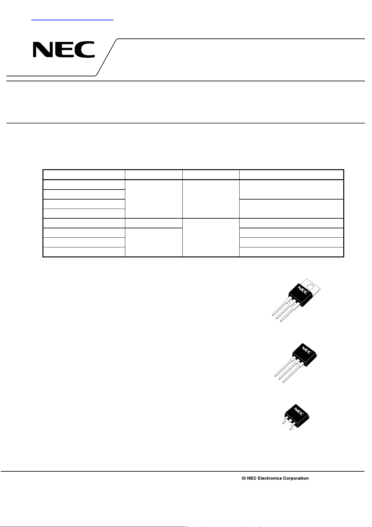
ORDERING INFORMATION
PART NUMBER LEAD PLATING PACKING PACKAGE
NP84N04EHE-E1-AY
NP84N04EHE-E2-AY
NP84N04KHE-E1-AY
NP84N04KHE-E2-AY
NP84N04CHE-S12-AZ
NP84N04DHE-S12-AY
NP84N04MHE-S18-AY
NP84N04NHE-S18-AY
Note1, 2
Note1, 2
Note1
Note1
Note1, 2
Note1, 2
Note1
Note1
Pure Sn (Tin) Tape 800 p/reel
Sn-Ag-Cu TO-220 (MP-25) typ. 1.9 g
50 p/tube
Pure Sn (Tin)
Tube
TO-263 (MP-25ZJ) typ. 1.4 g
TO-263 (MP-25ZK) typ. 1.5 g
TO-262 (MP-25 Fin Cut) typ. 1.8 g
TO-220 (MP-25K) typ. 1.9 g
TO-262 (MP-25SK) typ. 1.8 g
Notes 1. Pb-free (This product does not contain Pb in the external electrode.)
2. Not for new design
FEATURES
• Channel temperature 175 degree rated
• Super low on-state resistance
R
DS(on) = 5.2 mΩ MAX. (VGS = 10 V, ID = 42 A)
• Low input capacitance
C
iss = 4410 pF TYP.
• Built-in gate protection diode
(TO-220)
(TO-262)
(TO-263)
The information in this document is subject to change without notice. Before using this document, please
confirm that this is the latest version.
Not all products and/or types are available in every country. Please check with an NEC Electronics
sales representative for availability and additional information.
Document No. D14240EJ7V0DS00 (7th edition)
Date Published October 2007 NS
Printed in Japan
The revised points can be easily searched by copying an "<R>" in the PDF file and specifying it in the "Find what:" field.
1999, 2000, 2007
The mark <R> shows major revised points.

NP84N04EHE, NP84N04KHE, NP84N04CHE, NP84N04DHE, NP84N04MHE, NP84N04NH
E
ABSOLUTE MAXIMUM RATINGS (TA = 25°C)
Drain to Source Voltage (VGS = 0 V) VDSS 40 V
Gate to Source Voltage (V
Drain Current (DC) (T
Drain Current (Pulse)
Total Power Dissipation (T
Total Power Dissipation (T
Channel Temperature T
Storage Temperature T
Single Avalanche Current
Single Avalanche Energy
DS = 0 V) VGSS ±20 V
C = 25°C)
Note2
Note1
C = 25°C) PT 200 W
A = 25°C) PT 1.8 W
Note3
Note3
D(DC) ±84 A
I
D(pulse) ±336 A
I
ch 175 °C
stg −55 to +175 °C
AS 84/61/22 A
I
AS 70/372/484 mJ
E
Notes 1. Calculated constant current according to MAX. allowable channel temperature.
2. PW ≤ 10
3. Starting T
μ
s, Duty cycle ≤ 1%
ch = 25°C, VDD = 20 V, RG = 25 Ω, VGS = 20 → 0 V (see Figure 4.)
THERMAL RESISTANCE
Channel to Case Thermal Resistance Rth(ch-C) 0.75 °C/W
Channel to Ambient Thermal Resistance R
th(ch-A) 83.3 °C/W
2
Data Sheet D14240EJ7V0DS

NP84N04EHE, NP84N04KHE, NP84N04CHE, NP84N04DHE, NP84N04MHE, NP84N04NH
E
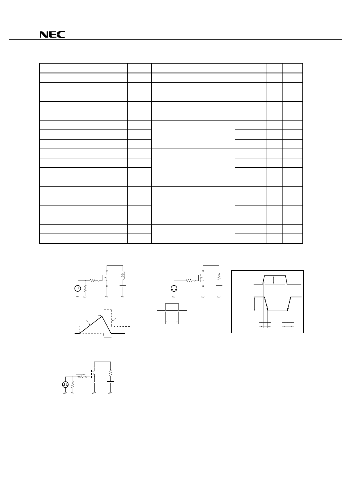
ELECTRICAL CHARACTERISTICS (TA = 25°C)
CHARACTERISTICS SYMBOL TEST CONDITIONS MIN. TYP. MAX. UNIT
Zero Gate Voltage Drain Current IDSS VDS = 40 V, VGS = 0 V 10
Gate Leakage Current IGSS VGS = ±20 V, VDS = 0 V ±10
μ
A
μ
A
Gate to Source Threshold Voltage VGS(th) VDS = VGS, ID = 250 μA 2.0 3.0 4.0 V
Forward Transfer Admittance | yfs | VDS = 10 V, ID = 42 A 20 47 S
Drain to Source On-state Resistance RDS(on) VGS = 10 V, ID = 42 A 4.6 5.2 mΩ
Input Capacitance Ciss 4410 6620 pF
Output Capacitance Coss 950 1430 pF
Reverse Transfer Capacitance Crss
Turn-on Delay Time td(on) 36 79 ns
Rise Time tr 25 62 ns
Turn-off Delay Time td(off) 77 150 ns
Fall Time tf
Total Gate Charge QG 87 130 nC
Gate to Source Charge QGS 20 nC
Gate to Drain Charge QGD
VDS = 25 V,
GS = 0 V,
V
f = 1 MHz
V
DD = 20 V, ID = 42 A,
V
GS = 10 V,
G = 1 Ω
R
VDD = 32 V,
GS = 10 V,
V
I
D = 84 A
490 890 pF
28 69 ns
32 nC
Body Diode Forward Voltage VF(S-D) IF = 84 A, VGS = 0 V 1.0 V
Reverse Recovery Time trr 49 ns
Reverse Recovery Charge Qrr
F = 84 A, VGS = 0 V,
I
μ
di/dt = 100 A/
s
60 nC
TEST CIRCUIT 1 AVALANCHE CAPABILITY
VGS = 20
PG.
→ 0
D.U.T.
G
= 25 Ω
R
50 Ω
V
BV
DSS
I
AS
I
D
V
DD
V
DS
Starting T
L
DD
V
ch
TEST CIRCUIT 3 GATE CHARGE
D.U.T.
G
= 2 mA
PG.
I
50 Ω
R
L
V
DD
TEST CIRCUIT 2 SWITCHING TIME
D.U.T.
R
PG.
V
GS
0
τ
μ
τ = 1 s
Duty Cycle ≤ 1 %
G
V
V
GS
Wave Form
V
DS
Wave Form
GS
10 %
0
V
DS
90 %
V
DS
0
t
d(on)
10 %10 %
trt
t
on
V
GS
d(off)tf
t
90 %
90 %
off
R
L
V
DD
Data Sheet D14240EJ7V0DS
3
 Loading...