PRELIMINARY DATA SHEET
GaAs MES FET
NES2527B-30
30 W S-BAND POWER GaAs FET
N-CHANNEL GaAs MES FET
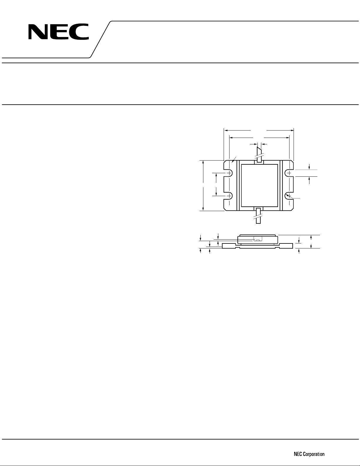
DESCRIPTION PACKAGE DIMENSIONS (UNIT: mm)
The NES2527B-30 is power GaAs FET which
provides high output power and high gain in the 2.5 - 2.7
GHz band.
Internal input matching circuits are designed to
optimize performance. The device has a 0.8 µm gate
length for increased linear gain. To reduce thermal
resistance, the device uses PHS (Plated Heat Sink)
technology.
The device incorporates WSi (tungsten silicide) gate
for high reliability and SiO2 glassivation for surface
stability.
FEATURES
• High output power
• High gain
• High power added efficiency
• Internally matched input
• High reliability
17.4±0.3 8.0
0.1
2.4
0.2 MAX
SOURCE
24±0.3
20.4
1.0±0.1
GATE
DRAIN
1.8
2.4
R1.2
4.5 MAX
QUALITY GRADE
Standard
Please refer to “Quality grade on NEC Semiconductor Devices” (Document number IEI-1209) published by NEC
Corporation to know the specification of quality grade on the devices and its recommended applications.
ABSOLUTE MAXIMUM RATINGS (TA = 25 °C)
Drain to Source Voltage V
Gate to Source Voltage V
Gate to Drain Voltage V
Drain Current I
Gate Current I
Total Power Dissipation P
Channel Temperature T
Storage Temperature T
Document No. P12381EJ1V0DS00 (1st edition)
Date Published February 1997 N
Printed in Japan
DS
GS
GD
D
G
T(*)
ch
stg
The information in this document is subject to change without notice.
15 V
7V
−
18 V
−
27 A
180 mA
110 W
175 °C
65 to +175 °C
−
C
= 25 °C
T
*
1997©

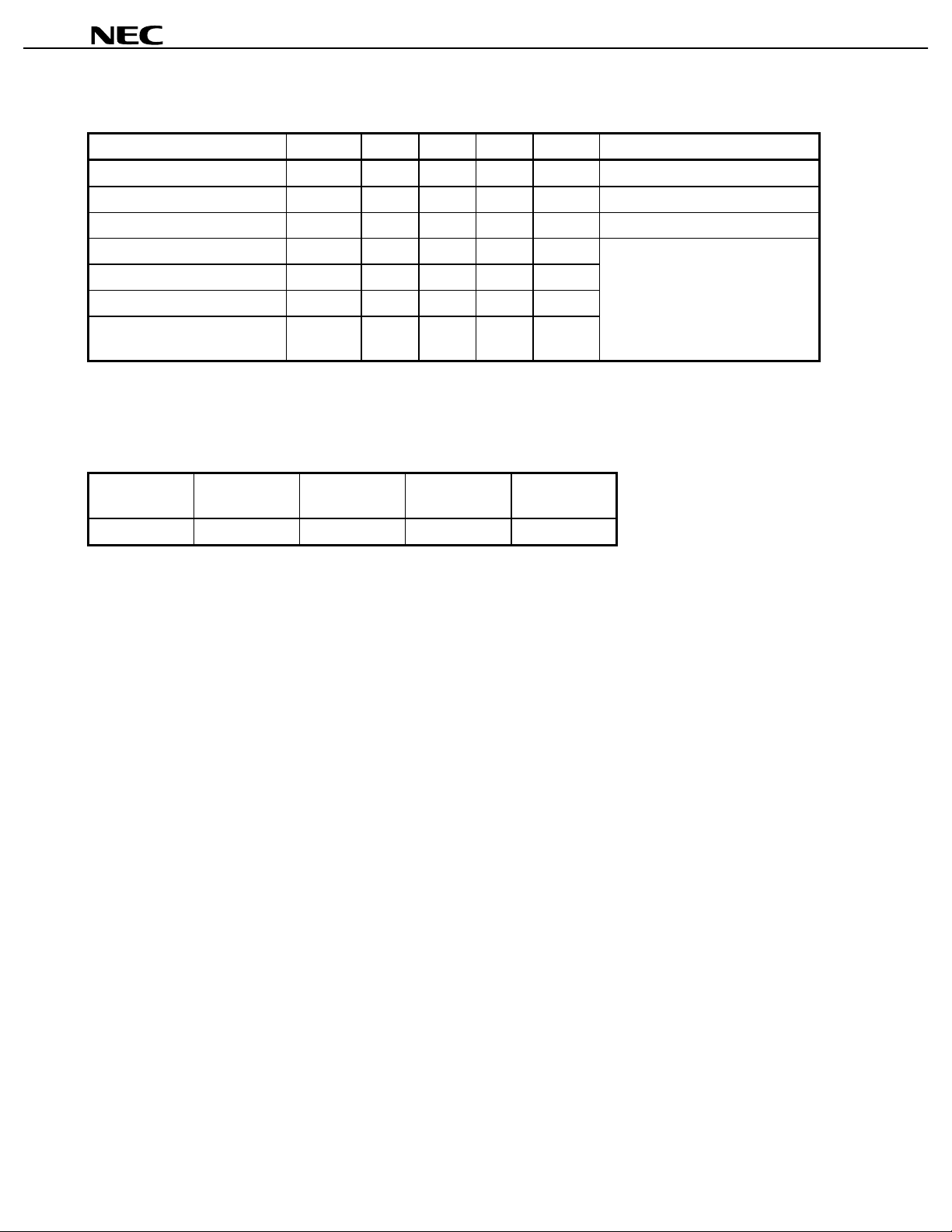
ELECTRICAL CHARACTERISTICS (TA = 25 °C)
CHARACTERISTICS SYMBOL MIN. TYP. MAX. UNIT TEST CONDITIONS
Saturated Drain Current Idss ðð 18.0 ðð AVDS = 2.5 V, VGS = 0 V
Pinch-off Voltage V
Thermal Resistance R
Output Power at 1 dB G.C.P
*3
Linear Gain G
Power Added Efficiency
3rd Order Intermodulation
P
th
1
Pð
L
K
add ðð 40.0 ðð %
*1
3
IM
ð4.0 ð2.6 ðð VVDS = 2.5 V, IDS = 80 mA
ðð 1.3 1.5 °C/W Channel to Case
44.0 45.0 ðð dBm
11.5 13.0 ðð dB
ðð ð42.0 ðð dBc
freq = 2.5/2.7 GHz
DS
= 10 V
V
DS
= 6.0 A (RF OFF)
I
Distortion
O
P
= 33.0 dBm, 'f = 1.0 MHz
*1
RECOMMENDING OPERATING LIMITS
*2
Rg
(:)
V
(V)
DS
Tch
(°C)
G.C.P
*3
Tcase
(°C)
NES2527B-30
30 to 10 to 130 to 3 dBcomp to 62
Rg is the series resistance between the gate supply and the FET gate.
*2
G.C.P: Gain Compression Point
*3
2
 Loading...