NEC NES1823P-100 Datasheet

PRELIMINARY DATA SHEET
N-CHANNEL GaAs MESFET
NES1823P-100
100W L-BAND PUSH-PULL POWER GaAs MESFET
DESCRIPTION
The NES1823P-100 is a 100 W push-pull type GaAs MESFET designed for high power transmitter applications for
IMT-2000 and PCS/PCN base station systems. It is capable of delivering 100 watts of output power with high linear
gain, high efficiency and excellent distortion. Its primary band is 1.8 to 2.3 GHz with different maching.
The device employs Tungsten Silicide gates, via holes, plated heat sink, and silicon dioxide and nitride
passivation for superior performance, thermal characteristics, and reliability.
Reliability and performance uniformity are assured by NEC’s stringent quality and control procedures.
FEATURES
• Push-pull type N-channel GaAs MESFET
• High Output Power : 100 W TYP.
• High Linear Gain : 11.0 dB TYP.
• High Drain Efficiency: 50 % TYP. @VDS = 10 V, I
Dset
= 6 A, f = 2.2 GHz
ORDERING INFORMATION (PLAN)
Part Number Package Supplying Form
NES1823P-100 T-92 ESD protective envelope
Remark
To order evaluation samples, please contact your local NEC sales office.
(Part number for sample order: NES1823P-100)
ABSOLUTE MAXIMUM RATINGS (TA = +25°C)
Operation in excess of any one of these parameters may result in permanent damage.
Parameter Symbol Ratings Unit
Drain to Source Voltage V
Gate to Source Voltage V
Drain Current I
Gate Current I
Total Power Dissipat i on P
Channel Temperature T
Storage Temperature T
DS
GSO
D
G
ch
stg
15 V
–7 V
76 A
440 mA
Note
T
220
175 °C
–65 to +175 °C
W
C
= 25°C
T
Note
Caution Please handle this device at static-free workstation, because this is an electrostatic sensitive
device.
Document No. P13839EJ1V0DS00 (1st edition)
Date Published November 1998 N CP(K)
Printed in Japan
The information in this document is subject to change without notice.
1998©

NES1823P-100
RECOMMENDED OPERATING LIMITS
Parameter Symbol Test Condition MIN. TYP. MAX. Unit
I
Dset
R
DSS
η
DS
ch
10.0 10.0 V
6.0 8.0 A
g
10 12.5 Ω
VDS = 2.5 V, VGS = 0 V 76 A
p
VDS = 2.5 V, IDS = 330 mA –4.0 –2.6 V
th
Channel to Case 0.6 0.8 °C/W
out
f = 2.2 GHz, VDS = 10 V
in
= +42.5 dBm, Rg = 12.5 Ω
P
D
Dset
= 6.0 A Total (RF OFF)
I
D
L
Note
49.0 50.0 dBm
20.0 32.5 A
50 %
9.0 11.0 dB
+150 °C
Drain to Source Voltage V
Gain Compression Gcomp 3.0 dB
Channel Temperature T
Set Drain Current
Gate Resistance
Notes 1.
Note 1
Note 2
Dset
I
= 3.0 A each drain, VDS = 10 V, RF OFF.
Rg is the series resistance between the gate supply and FET gate.
2.
ELECTRICAL CHARACTERISTICS (TA = +25°C)
Parameter Symbol Test Conditions MIN. TYP. MAX. Unit
Saturated Drain Current I
Pinch-off Voltage V
Thermal Resistance R
Output Power P
Drain Current I
Drain Efficiency
Linear Gain G
Note
Dset
I
= 3.0 A each drain
Preliminary Data Sheet2

TYPICAL CHARACTERISTICS (TA = +25°C)
POWER MATCHING AND IM3 MATCHING
NES1823P-100
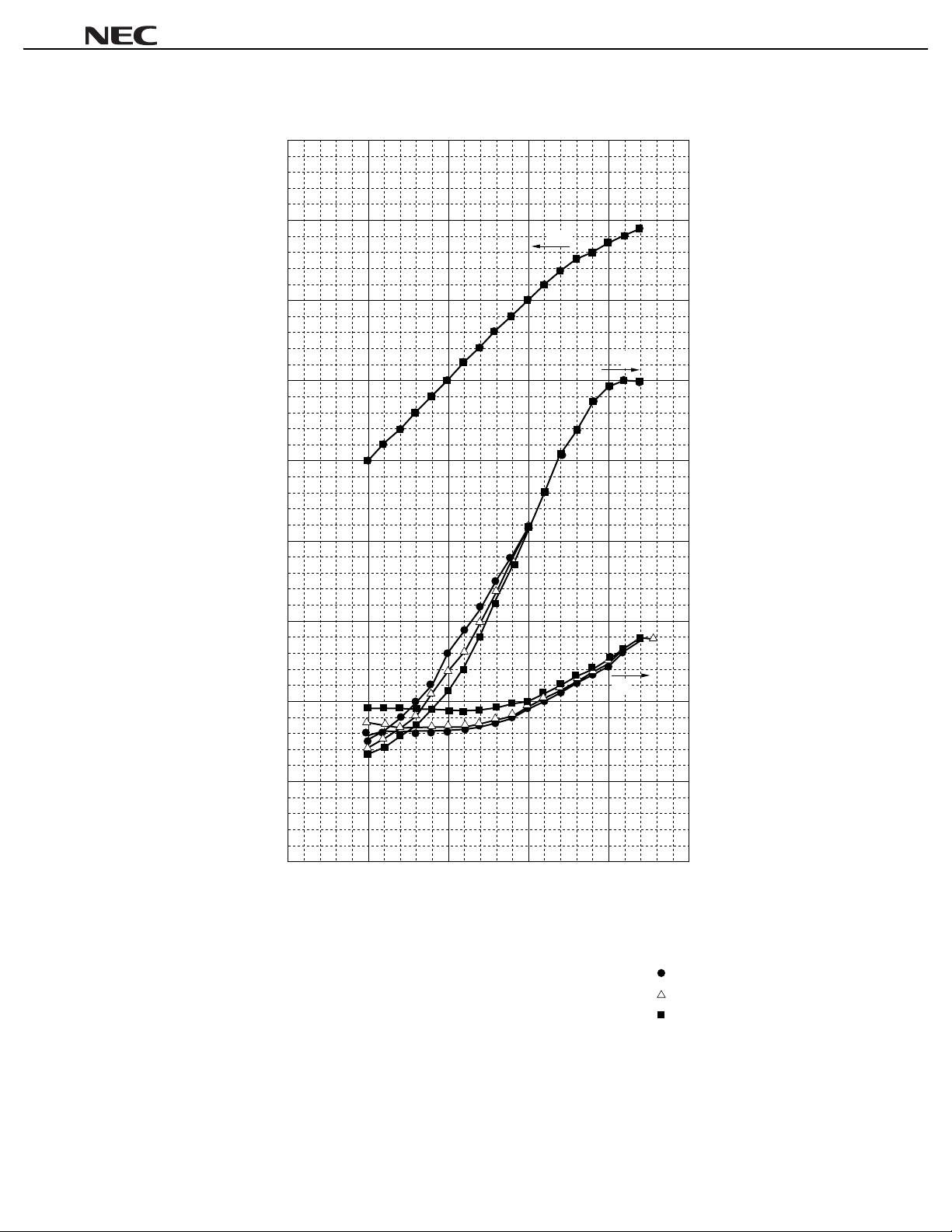
NEC produces two type matching circuits, power matching and IM
3
matching. Power matching circuit is used our
production line. And the IM3 matching circuit is useful for the customers to design the special tuning application. The
power matching is designed as this, input impedance is gain-matching, output is matched with power matching
impedance which is calculated with large signal simulation model. The IM3 matching is designed as this, input
impedance is matched to the impedance which has the direction of decreasing S21 phase-shift, output impedance is
matched to the almost same as the efficiency matching impedance. Those typical RF data are shown as this, GL =
10.2 dB P
out
= 50.0 dBm IM3 = –28 dBc at power matching, GL = 10.0 dB P
matching (@2 tone P
out
= 40 dBm).
out
= 49.3 dBm IM3 = –31 dBc at IM
3
Preliminary Data Sheet 3

NES1823P-100
55
50
45
40
35
(dBm)
out
30
Output Power P
OUTPUT POWER, DRAIN CURRENT AND EFFICIENCY
POWER MATCHING
vs. INPUT POWER
P
out
η
D
I
D
80
70
60
50
(%)
40
D
η
30
Drain Efficiency
(A)
D
Drain Current I
25
20
15
10
20 25 30 35 40 45
Input Power Pin (dBm)
V
DS
f
g
R
20
10
0
–10
= 10 V
= 2.2 GHz
= 12.5 Ω
Dset
= 2 A
I
Dset
= 4 A
I
Dset
= 6 A
I
Preliminary Data Sheet4

NES1823P-100
55
50
45
40
35
(dBm)
out
30
Output Power P
OUTPUT POWER, DRAIN CURRENT AND EFFICIENCY
DISTORTION MATCHING
vs. INPUT POWER
P
out
η
D
80
70
60
50
(%)
40
D
η
30
Drain Efficiency
(A)
D
Drain Current I
25
I
D
20
15
10
20 25 30 35 40 45
Input Power Pin (dBm)
V
DS
= 10 V
f
= 2.12 GHz
g
R
= 12.5 Ω
Dset
I
Dset
I
Dset
I
20
10
0
–10
= 6 A
= 8 A
= 10 A
Preliminary Data Sheet 5

NES1823P-100
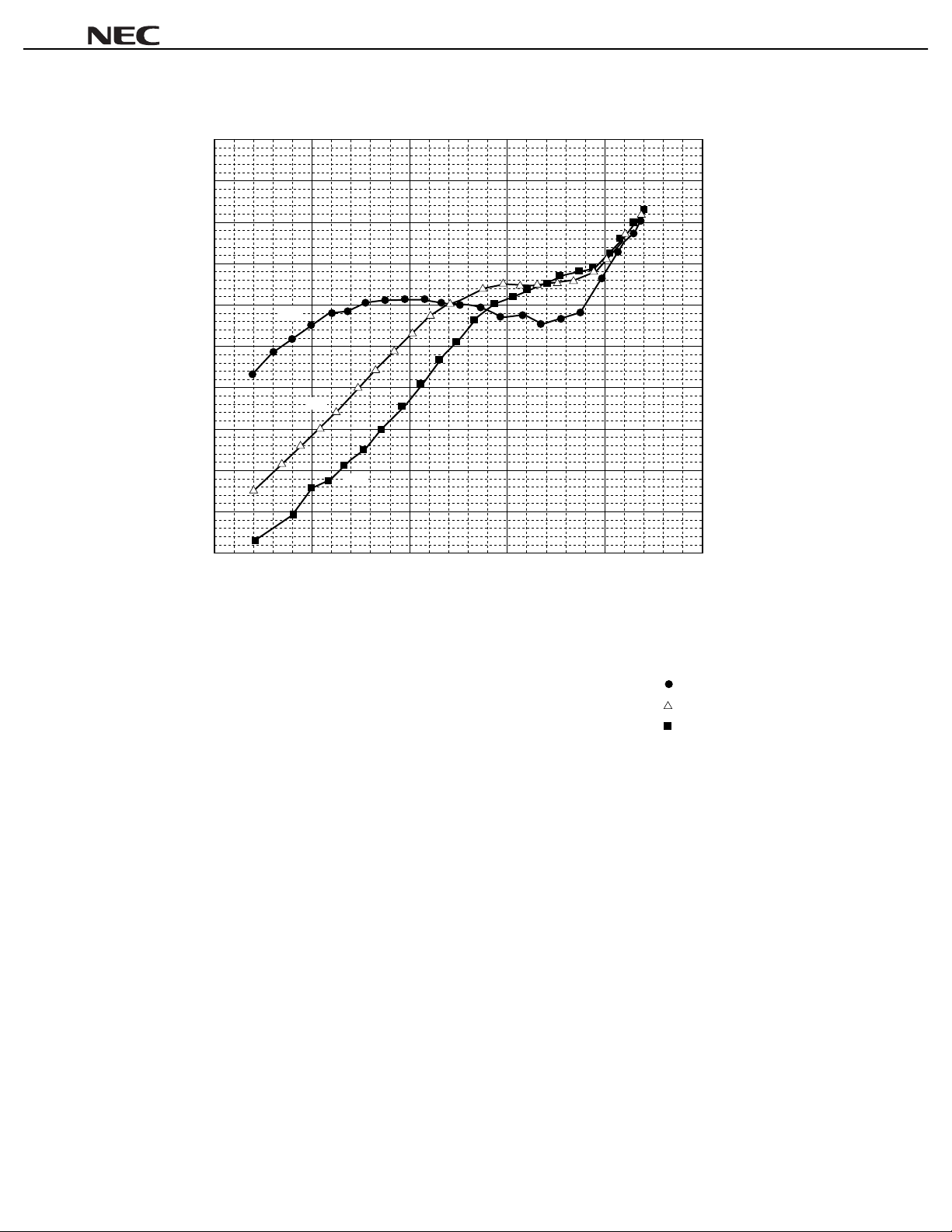
3rd INTERMODULATION DISTORTION vs.
2 TONES OUTPUT POWER
–10
–15
–20
(dBc)
3
–25
–30
2A
–35
–40
4A
3rd Intermodulation Distortion IM
–45
–50
–55
POWER MATCHING
6A
–60
25 30 35 40 45 50
2 tones Output Power P
out
(2 tones) (dBm)
V
f
∆
f
R
DS
g
= 10 V
= 1 MHz
= 2.2 GHz
= 12.5 Ω
Dset
= 2 A
I
Dset
= 4 A
I
Dset
= 6 A
I
Preliminary Data Sheet6
 Loading...