

Page 1

User’s Manual
EB-V850ES/HG2-EE
Demonstration Kit for the H_Line Family
Document No. EBV850ESHG2EE_V100
Date Published November 2005
NEC Electronics (Europe) GmbH
Page 2
EB-V850ES/HG2-EE
・
The information in this document is current as of date of its publication. The information is subject to
change without notice. For actual design-in, refer to the latest publications of NEC Electronics data
sheets or data books, etc., for the most up-to-date specifications of NEC Electronics products. Not all
products and/or types are available in every country. Please check with an NEC sales representative
for availability and additional information.
・
No part of this document may be copied or reproduced in any form or by any means without prior
written consent of NEC Electronics. NEC Electronics assumes no responsibility for any errors that
may appear in this document.
・
NEC Electronics does not assume any liability for infringement of patents, copyrights or other
intellectual property rights of third parties by or arising from the use of NEC Electronics products listed
in this document or any other liability arising from the use of such NEC Electronics products. No
license, express, implied or otherwise, is granted under any patents, copyrights or other intellectual
property rights of NEC Electronics or others.
・
Descriptions of circuits, software and other related information in this document are provided for
illustrative purposes in semiconductor product operation and application examples. The incorporation
of these circuits, software and information in the design of customer's equipment shall be done under
the ful l responsibility of customer. NEC Electronics no responsibility for any losses incurred by
customers or third parties arising from the use of these circuits, software and information.
・
While NEC Electronics endeavors to enhance the quality, reliability and safety of NEC Electronics
products, customers agree and acknowledge that the possibility of defects thereof cannot be
eliminated entirely. To minimize risks of damage to property or injury (including death) to persons
arising from defects in NEC Electronics products, customers must incorporate sufficient safety
measures in their design, such as redundancy, fire-containment and anti-failure features.
・
NEC Electronics products are classified into the following three quality grades: “Standard”, “Special”
and “Specific”.
The "Specific" quality grade applies only to NEC Electronics products developed based on a customerdesignated “quality assurance program” for a specific application. The recommended applications of NEC
Electronics product depend on its quality grade, as indicated below. Customers must check the quality
grade of each NEC Electronics product before using it in a particular application.
"Standard": Computers, office equipment, communications equipment, test and measurement
equipment, audio and visual equipment, home electronic appliances, machine tools,
personal electronic equipment and industrial robots.
"Special": Transportation equipment (automobiles, trains, ships, etc.), traffic control systems, anti disaster systems, anti-crime systems, safety equipment and medical equipment (not
specifically designed for life support).
"Specific": Aircraft, aerospace equipment, submersible repeaters, nuclear reactor control syste ms,
life support systems and medical equipment for li fe support, etc.
The quality grade of NEC Electronics products is “Standard” unless otherwise expressly specified in NEC
Electronics data sheets or data books, etc. If customers wish to use NEC Electronics products in
applications not intended by NEC Electronics, they must contact NEC Electronics sales representative in
advance to determine NEC Electronics 's willingness to support a given application.
Notes: 1." NEC Electronics" as used in this statement means NEC Electronics Corporation and also
includes its majority-owned subsidiaries.
2. " NEC Electronics products" means any product developed or manufactured by or for NEC
Electronics (as defined above).
M8E 02.10
2
Page 3
EB-V850ES/HG2-EE
CAUTION
This is a Test- and Measurement equipment with possibility to be significantly
altered by user through hardware enhancements/modifications and/or test or
application software. Thus, with respect to Council Directive 89/336/EEC
(Directive on compliance with the EMC protection requirements), this
equipment has no autonomous function. Consequently this equipment is not
marked by the CE-symbol.
Redemption of Waste Electrical and Electronic Equipment
(WEEE) in accordance with legal regulations applicable in the
European Union only: This equipment (including all
accessories) is not intended for household use. After use the
equipment cannot be disposed of as household waste. NEC
Electronics (Europe) GmbH offers to take back the equipment.
All you need to do is register at www.eu.necel.com/weee.
EEDT-ST-0005-10
3
Page 4

EB-V850ES/HG2-EE
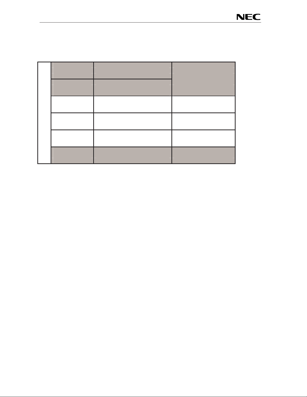
Revision History
Date Revision Chapter Description
16-11-2005 V1.00 --- First release
4
Page 5

EB-V850ES/HG2-EE
Table of Contents
1. Introduction .....................................................................................................................10
1.1 Main features of EB-V850ES/HG2-EE........................................................................................10
1.2 System requirements.................................................................................................................11
1.3 Package contents.......................................................................................................................11
1.4 Trademarks.................................................................................................................................11
2. EB-V850ES/HG2-EE system configuration....................................................................12
2.1 EB-V850ES/HG2-EE....................................................................................................................12
2.2 Host computer.. .... ... .... ... .... .... ... .... ... .... .... ... .... ... .... ... .... ... .... .... ... .... ... .... ... .... .... ... .... ... .... ...........12
2.3 Power supply via USB interface...... .... .... ... .... ... .... ... .... ... .... .... ... .... ... .... ... .... .... ... .... ... .... ....... ....12
3. EB-V850ES/HG2-EE board components........................................................................13
3.1 User button SW1 ........................................................................................................................14
3.2 User button SW2 ........................................................................................................................14
3.3 Configuration switch SW3. .... ... .... ... .... ... .... .... ... .... ... .... .... ... .... ... .... ... .... ... .... .... ... .... ... .... .... ... ....14
3.3.1 Normal operation mode.............................................................................................................14
3.3.2 On-Board debug mode..............................................................................................................14
3.3.3 FLASH programming mode.......................................................................................................15
3.3.4 N-Wire debugging mode............................................................................................................15
3.3.5 General-purpose switches......... .... ... .... ... .... .... ... .... ... .... ... .... .... ... ....... .... .... ... .... ... .... ... .... ... .... ....15
3.4 RESET button SW4....................................................................................................................15
3.5 Power LED LED1..... .... ... .... .... ... .... ... .... .... ... .... ... .... ... .... .... ... .... ... .... ... .... ... .... .... ... .... ... .... ... ........15
3.6 Power supply selector JP1....... .... ... .... ... .... .... ... .... ... .... ... .... .... ... .... ... .... .... ... .... ... .... ... .... ... .... ....16
3.7 External power supply...............................................................................................................16
3.8 USB interface connector USB1..................................................................................................17
3.9 N-Wire connectors NWIRE1, NWIRE2........................................................................................18
3.10 External LED U2....................... .................................................................................................20
3.11 External connectors CN1 and CN2..........................................................................................21
3.12 Soldering Bridges ....................................................................................................................24
3.13 V850ES/HG2 memory map............................................................................................ ...........25
4. EB-V850ES/HG2-EE installation and operation.............................................................26
4.1 Getting started............................................................................................................................26
4.1.1 CD-ROM contents.....................................................................................................................26
5. Hardware installation ......................................................................................................27
6. Software installation........................................................................................................27
6.1 IAR Systems Embedded Workbench for V850 installation ......................................................27
6.2 FPL FLASH programming GUI installation...............................................................................27
6.3 Sample program installation ................................................... ..................................................27
6.4 USB Driver Installation...............................................................................................................28
6.4.1 Installation on Windows 98SE/Me..............................................................................................28
6.4.2 Installation on Windows 2000 ....................................................................................................30
6.4.3 Installation on Windows XP .......................................................................................................36
6.5 Confirmation of USB Driver Installation ...................................................................................41
5
Page 6

EB-V850ES/HG2-EE
6.6
Driver Uninstallation ..................................................................................................................42
7. FPL FLASH programming software................................................................................ 44
7.1 Introduction................................................................................................................................44
7.2 Starting up the GUI Software.....................................................................................................44
7.3 Toolbar........................................................................................................................................45
7.4 Menu Bar........... .... ... .... ... .... .... ... .... ... .... ... .... .... ... .... ... .... .... ... ....... .... ... .... ... .... .... ... .... ... . ..............46
7.4.1 [Fil e] menu ... ... .... ... .... ... .... .... ... .... ... .... .... ... ....... .... ... .... ... .... .... ... .... ... .... ... .... .... ... .... ... .... ...........46
7.4.2 [Device] menu...........................................................................................................................47
7.4.3 [View] menu ..............................................................................................................................54
7.4.4 [Help] menu .. ... .... ... .... ... .... ....... .... ... .... ... .... .... ... .... ... .... .... ... .... ... .... ... .... .... ... .... ... .... ... .... ...........55
7.5 Programmer Parameter Window ......................................................................... ......................56
8. How to use FPL FLASH programming software............................................................ 57
(1) Installing the FPL GUI software.....................................................................................................57
(2) Installing the driver........................................................................................................................57
(3) Installing the parameter file...........................................................................................................57
(4) Connecting and starting................................................................................................................58
(5) Setting the programming environment ..........................................................................................59
(6) Selecting a user program..............................................................................................................62
(7) [Autoprocedure(EPV)] command execution...................................................................................63
(8) Terminating the GUI .....................................................................................................................63
(9) Execute “CountDownTimer” application ............. ... .... ... .... .... ... .... ... .... ... .... ... .... .... ... .... ... .... ... .... ....63
(10) Restarting the GUI......................................................................................................................63
9. TROUBLESHOOTING......................................................................................................64
10. On-Board debugging..................................................................................................... 66
10.1 Monitor resources............ .... ... .... ... .... .... ... .... ... .... ... .... .... ... .... ... .... ... .... ... .... .... ... .... ... .... ... ........67
10.1.1 UARTA0..................................................................................................................................67
10.1.2 Interrupt vectors ... .... ... .... .... ... .... ... .... .... ... .... ... .... ... .... .... ... .... ... ....... .... ... .... .... ... .... ... .... ... ........67
10.1.3 Reset vector ............................................................................................................................68
10.1.4 Memory area..... ... .... .... ... .... ... .... ... .... ... .... .... ... .... ... .... .... ... .... ... .... ... .... .... ... .... ... .... ... .... ... ........68
10.1.5 Clock oper ation..... .... ... .... .... ... .... ... .... .... ... .... ... .... ... .... .... ... .... ... .... ... .... ... .... .... ... .... ... .... ... ........68
10.1.6 Other limitations ... .... ... .... .... ... .... ... .... .... ... .... ... .... ... .... .... ... .... ... .... ... .... ... .... .... ... .... ... .... ... ........68
10.2 IAR sample session... ... .... .... ... .... ... .... ....... .... ... .... ... .... ... .... .... ... .... ... .... ... .... ... .... .... ... .... ... ........69
11. Sample programs..........................................................................................................75
11.1 General Introduction........ .... ... .... ... .... ... .... .... ... .... ... .... ... .... .... ... .... ... .... .... ... .... ... .... ... .... ... ........75
11.2 Count Down Timer ............... ... .... ... .... ... .... .... ... .... ... .... ... .... .... ... .... ... .... ... .... .... ... .... ... .... .... ... ....76
11.3 Electronic Dice .........................................................................................................................76
11.4 Entrance code checker.............................................................................................................77
11.5 Lightshow .................................................................................................................................77
11.6 Melody maker ....................................................................................... ....................................78
11.7 Reaction time measurement....................................................................................................78
12. Cables ............................................................................................................................79
12.1 USB interface cable (Mini-B type).......... ... .... ... .... ... .... ... .... .... ... .... ... .... ... .... .... ... .... ... .... ... .... ....79
6
Page 7

EB-V850ES/HG2-EE
13. Schematics ....................................................................................................................80
7
Page 8

EB-V850ES/HG2-EE
List of Figures
Fig u re 1: EB-V850ES/HG2-EE system configuration.............................................................................12
Fig u re 2: EB-V850ES/HG2-EE board connectors, switches and LED’s....... ... .... ... .... ... .... .... ... .... ... .... .... 13
Figure 3: Connector USB1, USB Mini-B Type Host Connector Pin Configuration.. .... .... ... .... ... .... ... .... .... 17
Figure 4: On-chip debugging system configuration ................................................................................18
Figure 5: External connectors CN1 and CN2.............. ...........................................................................21
Figure 6: Placement of soldering bridges............................................................................................... 24
Figure 7: Add New Hardware Wizard (Windows 98SE).........................................................................28
Figure 8: Search Method (Windows 98SE)............................................................................................28
Figure 9: Search Location Specification (Windows 98SE)......................................................................29
Figure 10: Checking Driver to Be Installed (Windows 98SE)..................................................................29
Figure 11: Installation Completion (Windows 98SE) ........................................................ ...................... 30
Figure 12: Found New Hardwar e W izard 1 (Wi ndows 2000). .... ... .... .... ... .... ... .... .... ... ....... .... ... .... .... ... .... 30
Figure 13: Search Method 1 (Windows 2000)............. ... .... ... .... .... ... .... ... .... ... .... ... .... .... ... .... ... .... ... .... .... 31
Figure 14: Driver File Location 1 (Windows 2000) .................................................................................31
Figure 15: Address Specification 1 (Wi ndows 2000)............. .... ... .... .... ... .... ... .... .... ... .... ... .... ... .... ... .... .... 32
Figure 16: Driver File Search 1 (Windows 2000) ...................................................................................32
Figure 17: USB Driver Installation Completion 1 (Windows 2000)........... .... ... .... ... .... .... ... .... ....... ... .... .... 33
Figure 18: Found New Hardwar e W izard 2 (Wi ndows 2000). .... ... .... .... ... .... ... .... .... ... ....... .... ... .... .... ... .... 33
Figure 19: Search Method 2 (Windows 2000)............. ... .... ... .... .... ... .... ... .... ... .... ... .... .... ... .... ... .... ... .... .... 34
Figure 20: Driver File Location 2 (Windows 2000) .................................................................................34
Figure 21: Address Specification 2 (Windows 2000).......... ... .... ... .... .... ... .... ... .... .... ... .... ... .... ... .... ... .... .... 35
Figure 22: Driver File Search 2 (Windows 2000) ...................................................................................35
Figure 23: USB Driver Installation Completion 2 (Windows 2000)........... .... ... .... ... .... .... ... .... ....... ... .... .... 36
Figure 24: Found New Hardwar e W izard 1 (Wi ndows XP ).... .... .... ... .... ... .... ... .... ... .... .... ... .... ... .... ... .... .... 36
Figure 25: Search Location Specification 3 (Windows XP).....................................................................37
Figure 26: Windows XP Logo Testing 3 (Windows XP).......................................................................... 37
Figure 27: USB Driver Installation Completion 1 (Windows XP ) .... ... .... ... .... ... .... .... ... .... ... .... ... .... ....... .... 38
Figure 28: Found New Hardware Wizard 2 (Windows XP)........ .... ... .... ... .... ... .... ... .... .... ... .... ... .... ... .... .... 38
Figure 29: Search Location Spec ification 2 (Windows XP)........ .... ... .... ... .... ... .... ... .... .... ... .... ... .... ... .... .... 39
Figure 30: Windows XP Logo Testing 2 (Windows XP).......................................................................... 39
Figure 31: USB Serial Port2 Driver Installation Completion (Windows XP) ............................................ 40
Figure 32: Device Manager ................................................................................................................... 41
Figure 33: Driver Uninstallation ............................................................................................................. 42
Figure 34: Driver Uninstaller................................................................................. ................................. 42
Figure 35: Completion of Driver Uninstallation....................................................................................... 43
Figure 36: GUI Software Main Window.................................................................................................. 44
Figure 37: Toolbar Buttons....................................................................................................................45
Fig u re 38 : [ F ile] Menu ....................................................................................................................... .... 46
Figure 39: HEX Fil e Selection Window . .... ... .... .... ... .... ... .... ... .... ... .... .... ... .... ... .... .... ... .... ... .... ... .... .... .......46
Fig u re 40 : [ D evice] Menu ......................................................................................................................47
Figure 41: Device Setup Window - Standard.........................................................................................49
Figure 42: Setup Window - Parameter File Selection............................................................................. 50
Figure 43: Parameter File Selection Window.........................................................................................50
Figure 44: Setup Window - Communication interface to device.............................................................51
Figure 45: Setup Window - Supply Oscillator Selection ....................................................... ..................51
Figure 46: Setup Window - Operation Mode..........................................................................................52
Figure 47: Device Setup Window - Advance................................................................. .........................53
Figure 48: Setup Window - Command options.......................................................................................53
Fig u re 49 : [ V iew] Menu.......................................................................................................................... 54
Fig u re 50 : [ H elp] Menu.......................................................................................................................... 55
Figure 51: About FPL Window............................................................................................................... 55
Figure 52: Programmer Parameter W indow ........... .... ... .... ... .... ... .... .... ... .... ... .... ... .... .... ... .... ... .... ... .... ....56
Figure 53: GUI Software Startup Screen.......... .... ... .... ... .... ... .... ... .... .... ... .... ... .... ... .... .... ... .... ... .... ... .... .... 59
Figure 54: <Standard Device Setup> Dialog Box...................................................................................59
Figure 55: Parameter File Selection ......................................................................................................60
Figure 56: Port Selection...................................................................................................... .................60
Figure 57: <Standard Device Setup> Dialog Box after Setting............................................................... 61
Figure 58: <Advance Device Setup> Dialog Box...................................................................................61
8
Page 9

EB-V850ES/HG2-EE
Page 10

EB-V850ES/HG2-EE
1. Introduction
EB-V850ES/HG2-EE is a demonstration kit for the NEC’s H_Line V850ES microcontroller family. It
supports On-Board debugging, FLASH programming and real time execution of application programs.
The board is prepared to be connected to user hardware parts such as digital I/O or analogue signals.
1.1 Main features of EB-V850ES/HG2-EE
• Easy to use device demonstration capabilities
EB-V850ES/HG2-EE contains elements to easily demonstrate simple I/O-functions, i.e. push buttons,
7 segment LED output, AD reference voltage, I/O lines, UART serial interface.
• Power supply via USB interface
EB-V850ES/HG2-EE is powered via USB interfac e, no separate power supply is needed.
• On-Board debug function
The EB-V850ES/HG2-EE supports an On-Board debug function by using the IAR C-SPY debugger,
without a need of additional debug hardware. It allows FLASH programming and supports standard
debug functions i.e. code execution, single stepping, software breakpoints, memory manipulation etc.
• N-Wire debugging
The EB-V850ES/HG2-EE is prepared to be equipped with a KEL adapter in order to connect the QBV850MINI-EE or IE-V850E1-CD-NW On-Chip debug emulator to use On-Chip debug function of the
V850ES/HG2 device. Please note, the QB-V850MINI-EE and IE-V850E1-CD-NW are separate
products from NEC and there are not included in this starterkit package.
• FPL, FLASH programming software
A windows based FLASH programming software allows to select and download application programs
to the EB-V850ES/HG2-EE board for evaluation purposes.
• Analogue to digital signal conversion is supported
• Vari ous input / out put signals available, such as
° All I/O ports prepared to be connected to user hardware
° Timer input / output signals
° Two or three wire serial I/O
° UART interface, via USB UART chip FT232
° 16 analogue input lines
° 7 segment LED
° 2 push buttons prepared for external interrupt generation
• The IAR Embedded Workbench for V850 and the IAR C-SPY debugger / simulator are included.
These packages are restricted in such that maximum program code size is limited to 16 kByte.
• Full documentation is included for the NEC V850ES/HG2 device, the IA R Systems Embedded
Workbench, IAR Systems C-SPY debugger / simulator and the NEC FPL FLASH programming
software.
EB-V850ES/HG2-EE is not intended for code development. NEC does not allow and does not
support in any way any attempt to use EB-V850ES/HG2-EE in a commercial or technical product.
10
Page 11

EB-V850ES/HG2-EE
1.2 System requirements
HOST PC
Host interface
1.3 Package contents
Please verify that you have received all parts listed in the package contents list attached to the
EB-V850ES/HG2-EE p a c k a ge . I f any pa rt is mi ssing or see ms to be da maged , plea se co ntact t h e de aler
fro m whom yo u r ec e i ved yo ur EB-V850ES/HG2-EE starterkit.
Note:
Updates to this User Manual, additional documentation and/or utilities for EB-V850ES/HG2-EE
starterkit, if available, may be downloaded from the NEC WEB page(s) at
http://www.eu.necel.com/updates.
A PC supporting Windows 98SE, Windows ME, Windows 2000 or
Windows XP is required for the IAR Systems Embedded Workbench
demo-version and the FPL FLASH programming software.
Pentium 166 MHz (at least), 128 MB of RAM, 256-color display (1024 *
768), mouse, CD-ROM drive and 200 Mbytes of free hard disk space are
required to install the tool packages.
Above listed requirements are valid for the IAR Systems Embedded
Workbench and the FPL FLASH programming software.
USB interface that enables communication based on USB (Ver1.1 or
later)
1.4 Trademarks
IAR Embedded Workbench, visualSTATE, IAR MakeApp and C-SPY are registered trademarks of IAR
Systems AB. Microsoft and Windows are registered trademarks of Microsoft Corporation. Adobe and
Acrobat Reader are registered trademarks of Adobe Systems Incorporated.
All other product names are trademarks or registered trademarks of their respective owners.
11
Page 12
EB-V850ES/HG2-EE
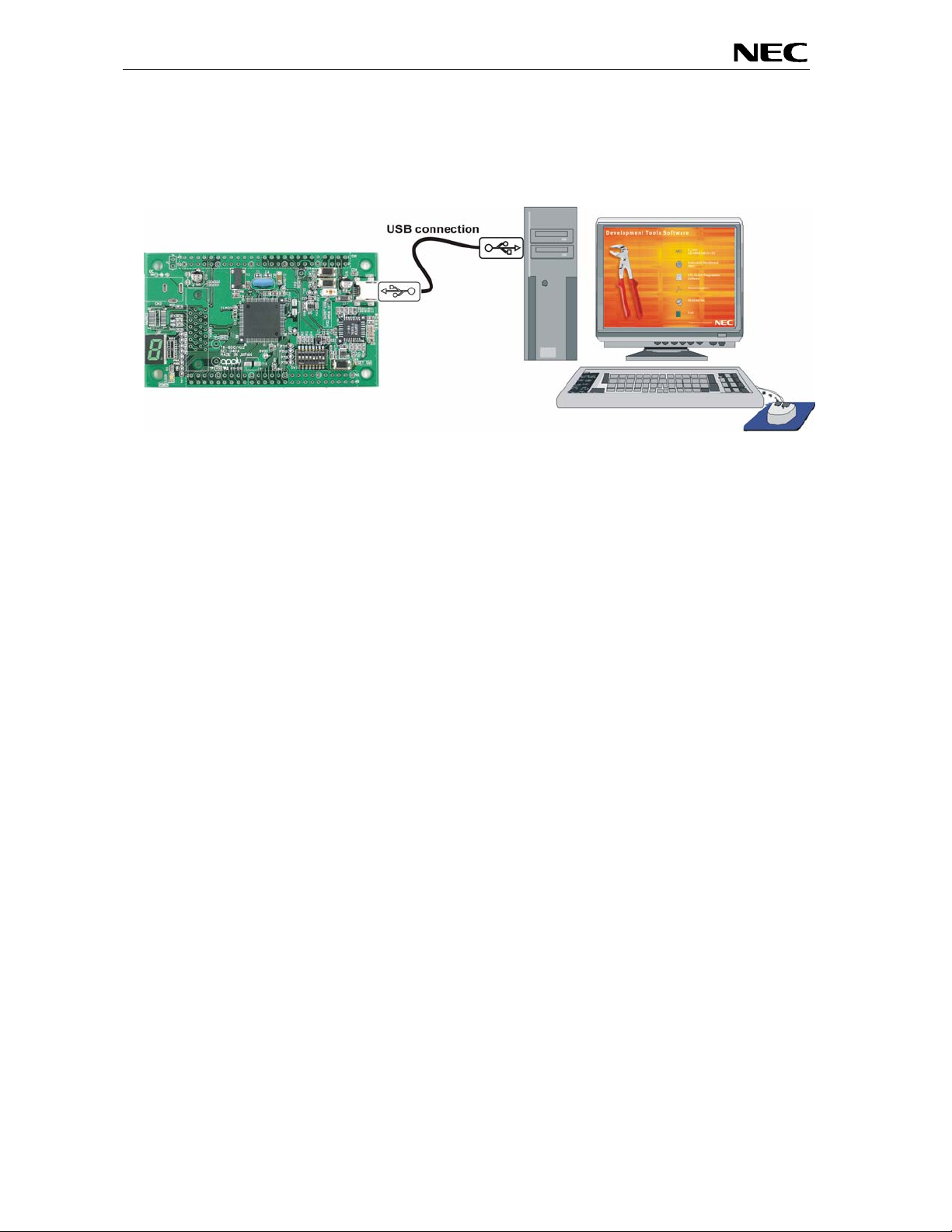
2. EB-V850ES/HG2-EE system configuration
The EB-V850ES/HG2-EE system configuration is given in the diagram below:
Figure 1: EB-V850ES/HG2-EE system configuration
2.1 EB-V850ES/HG2-EE
EB-V850ES/HG2-EE is a demonstration kit for the NEC H_Line V850ES family devices. As a typical
microcontroller from H_Line family the V850ES/HG2 device (µPD70F3707) is used. The board is
connected to the host system via a USB interface cable. The host system may be used for On-Boa rd
debugging or FLASH programming and to allow execution of application programs on the V850ES/HG2
device.
The EB-V850ES/HG2-EE board is equipped with an 5.0000 MHz oscillator, allows running the
V850ES/HG2 microcontroller at 20MHz. Sub-clock is provided with 32.768 kHz.
2.2 Host computer
The USB host interface enables communication to the EB-V850ES/HG2-EE board. Th e USB UART chi p
FT232 allows application software to access the USB device in the same way as it would access a
standard RS232 interface. The FTDI's Virtual COM Port (VCP) driver appears to the windows system as
an extra Com Port, in additi on to any existing hardware Com Ports.
2.3 Power supply via USB interface
EB-V850ES/HG2-EE is powered by USB interface, no separate power supply is needed. The USB
interface provides the EB-V850ES/HG 2-EE board with 5V supply voltage.
12
Page 13
EB-V850ES/HG2-EE
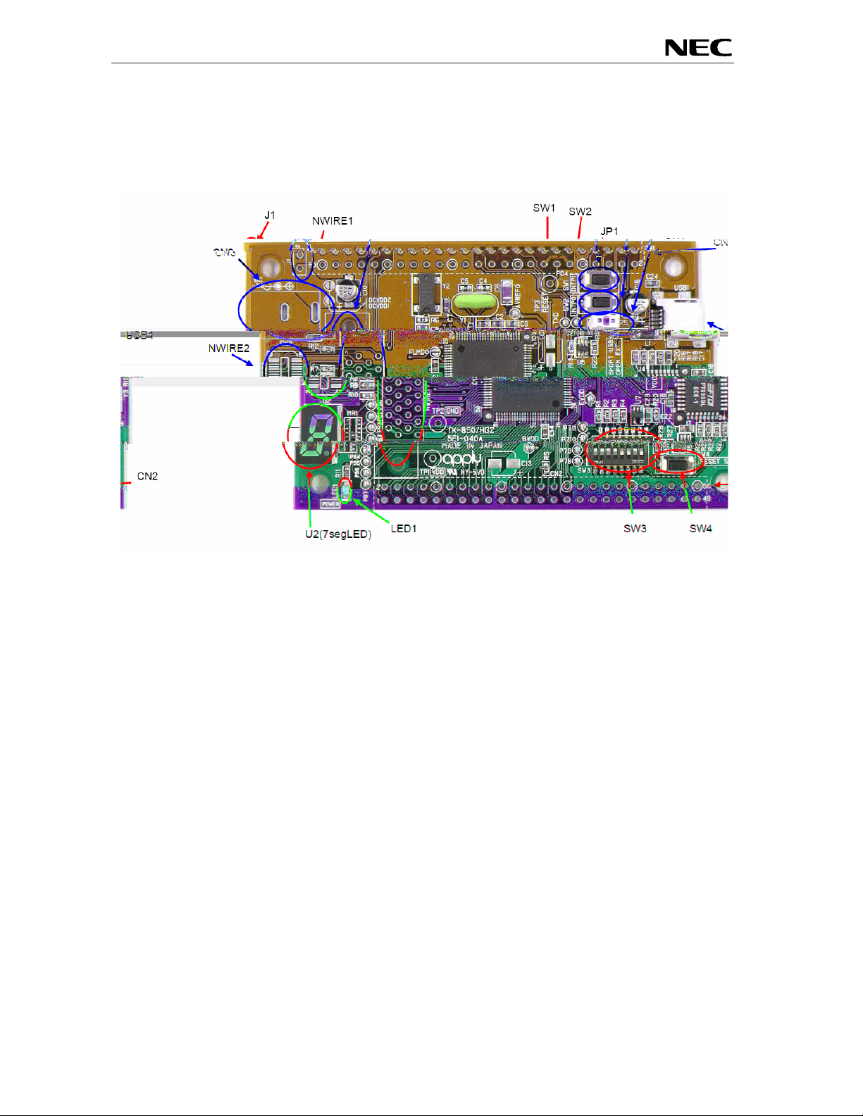
3. EB-V850ES/HG2-EE board components
The EB-V850ES/HG2-EE board is equipped with push buttons, a 7 segment LED and several connectors
in order to be connected to user hardware or host computers.
Figure 2: EB-V850ES/HG2-EE board connectors, switches and LED’s
Some of the EB-V850ES/HG2-EE components are free for user application hardware and software.
Please read the user’s manual of the V850ES/HG2 device carefully to get information about the
electrical specification of the available I/O ports before you connect any external signal to the EB-
V850ES/HG2-EE board.
13
Page 14

EB-V850ES/HG2-EE
3.1 User button SW1
SW 1 i s a pus h bu tt o n c on necting VS S to ext e rna l inte r r u pt i n pu t I NT P1 of the m icr oc o ntrolle r . Th i s is
equal to port P04 of the V850ES/HG2 device. The port may be programmed to generate interrupt INTP1.
The necessary initialisation for this purpose is described in the user’s m anual of the V850ES/HG2 device.
Please note, when using SW1 turn ON the built-in pull-up resistor of V850ES/HG2 device, register PU0.
3.2 User button SW2
SW 2 i s a pus h bu tt o n c on necting VS S to ext e rna l inte r r u pt i n pu t I NT P0 of the m icr oc o ntrolle r . Th i s i s
equal to port P03 of the V850ES/HG2 device. The port may be programmed to generate interrupt INTP0.
The necessary initialisation for this purpose is described in the user’s m anual of the V850ES/HG2 device.
Please note, when using SW2 turn ON the built-in pull-up resistor of V850ES/HG2 device, register PU0.
3.3 Configuration switch SW3
The dip-switch SW3 (Bits 1-4) controls the different operating modes of the EB-V850ES/HG2-EE board.
The Bits 5-8 of dip-switch SW3 are for general-purpose input and are connected to the ports P78~P711
of t h e m icr oc o nt rol l e r .
14
Page 15
EB-V850ES/HG2-EE
3.3.3 FLASH programming mode
For programming of the built-in FLASH memory of the V850ES/HG2 device by using the FPL FLASH
programming GUI please configure switch SW 3 as following:
SW3 Configuration
Bit 1 ON
Bit 2 OFF
Bit 3 ON
Bit 4 ON
Table 3: SW3, FLASH program m ing m ode
3.3.4 N-Wire debugging mode
To enable N-Wire On-Chip debugging by using the QB-V850MINI-EE or IE-V850E1-CD-NW On-Chip
debug emulators please configure switch SW3 of the EB-V850ES/HG2-EE board as following:
SW3 Configuration
Bit 1 OFF
Bit 2 OFF
Bit 3 OFF
Bit 4 OFF
Table 4: SW3, N-Wire debugging mode
Please refer also to CHAPTER 3.9 N-WIRE CONNECTORS NWIRE1, NWIRE2 of this document.
3.3.5 General-purpose switches
The Bits 5-8 of dip-switch SW3 are for general-purpose inputs and are c onnected to the ports P78~P711
of the microcontroller. Switching Bits 5-8 to ON applies VSS to the corresponding port of the
microcontroller. Switching Bits 5-8 to OFF applies VDD to the corresponding port.
SW3 V850ES/HG2
Bit 5 P78
Bit 6 P79
Bit 7 P710
Bit 8 P711
Table 5: SW3, general-purpose switches
3.4 RESET button SW4
SW4 is a reset button. It activates the power on reset. It is connected to the reset circuit of the
EB-V850ES/HG2-EE board.
3.5 Power LED LED1
LED1 is the Powe r LED. LED1 is activated if power is supplied to the EB-V850ES/HG2-EE board.
15
Page 16
EB-V850ES/HG2-EE
3.6 Power supply selector JP1
Jumper JP1 selects the power supply of the EB-V850ES/HG2-EE board. Closing jumper JP1 (default
setting) supplies power (VCC = 5V) from the USB interface line. When opening JP1, external power can
be supplied by using connectors CN3 or J1.
JP1 Mode
closed (default) Power supplied by USB interface
open External power supply
Table 6: Power supply selector, JP1
Note: When choosing external power supply, please open jumper JP1!
3.7 External power supply
External power can be supply by connecting a 5V AC adapter to connector CN3 (not assem bled). Per
def ault, the ex ternal power is s uppli ed to th e connect or CN1 only ( pins 10, 12 a nd 16) . To power th e
com plet e bo ard v i a exte r na l po wer supp ly, t he sol d erin g br idge s DCVDD1 and D CV D D2 m us t be cl o sed .
CN3 Function
Center (1) Vcc = 5V
Ring (2,3) Gnd
Table 7: External power supply, connector CN3
Additionally a stabilizing 5V power supply can be connected directly to the connector J1 i nstead of using
a 5V AC adapter. Also in this case the soldering bridges DCVDD1 and DCVDD2 must be closed.
Note: When using an external power supply, please open jumper JP1!
J1 Function
1 Vcc = 5V
2 Gnd
Table 8: External power supply, connector J1
16
Page 17
EB-V850ES/HG2-EE
3.8 USB interface connector USB1
USB1 connector allows connecting the IAR C-SPY debugger or the F PL FLASH programming software
to the EB-V850ES/HG2-EE board in order to debug or program application software to the V850ES/HG2
device. The board power supply of 5V is also provided by this connector.
Additionally connector US B1 connects UARTA0 of the V850ES/HG2 device to the host system.
1
Figure 3: Connector USB1, USB Mini-B Type Host Connector P in Configurati on
USB Co nn ec t o r
USB1
1 VBUS
2 D3 D+
4 N.C.
5 GND
Table 9: Pin Configuration of USB Connector USB1
For connection with the host machine, use a USB cable (Mini-B type). For confirmation, NEC Electronics
used only the USB cable delivered with the EB-V850ES/HG2-EE board.
5
Signal Name
17
Page 18
EB-V850ES/HG2-EE
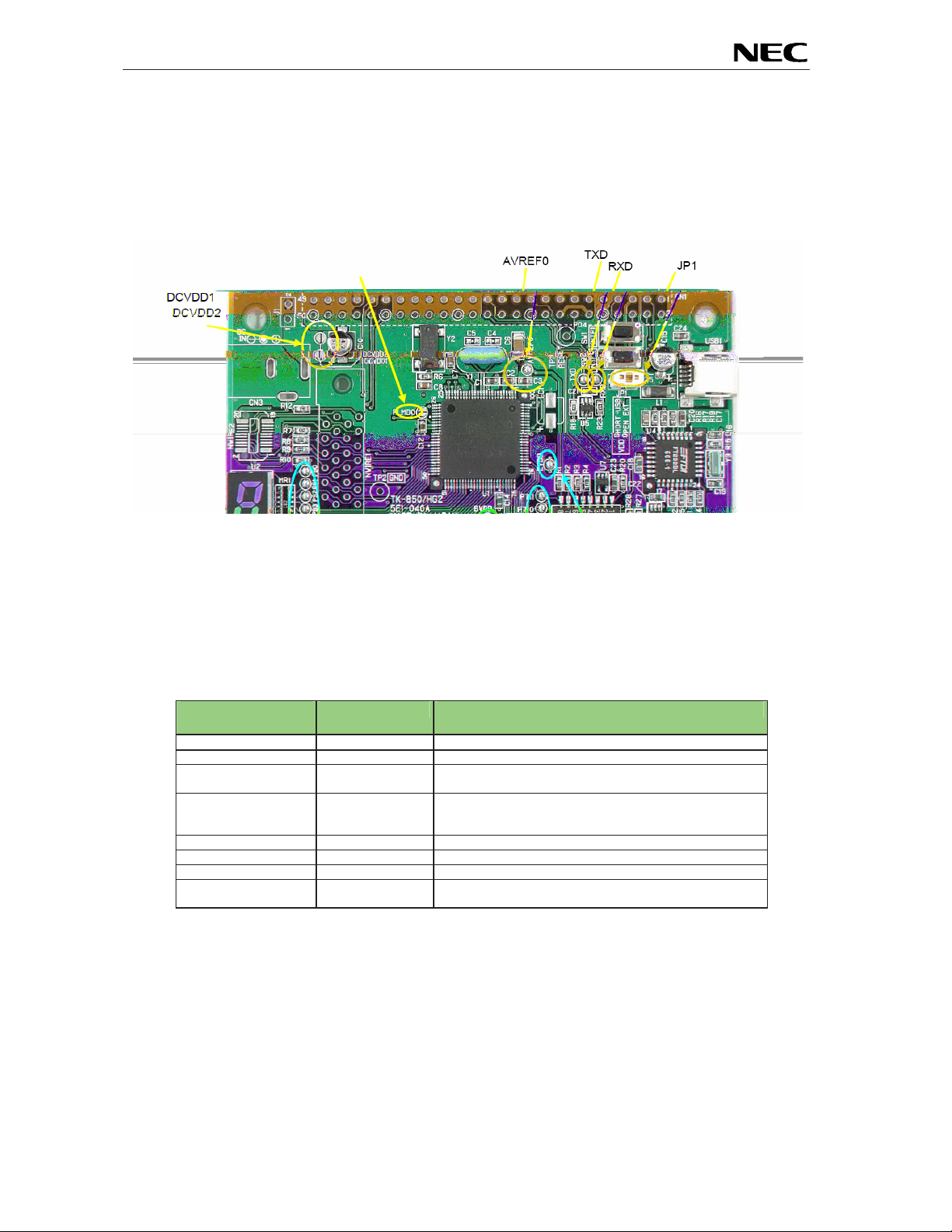
3.9 N-Wire connectors NWIRE1, NWIRE2
The NWIRE1 and NWIRE2 connectors (not assembled) do allow the connection of the QB-V850MINI-EE
or alternative the IE-V850E1-CD-NW On-Chip debug emulators to the EB-V850ES/HG2-EE board in
orde r to use On-Chip debug function (N-Wire) of the V850ES/HG2 device.
IE-V850E1-CD-NW Laptop/Desktop PC
alternative
USB cable
QB-V850MINI-EE
Figure 4: On-chip debugging system configurati on
N-Wire I/F
cable
EB-V850ES/HG2-EE
Please note that the QB-V850MINI-EE and IE-V850E1-CD-NW are separate products from NEC and are
not included in this starterkit package.
To enable On-Chip debugging via N-Wire please configure switch SW3 of the EB-V850ES/HG2-EE
boar d as following:
SW3 Configuration
Bit 1 OFF
Bit 2 OFF
Bit 3 OFF
Bit 4 OFF
18
Page 19
EB-V850ES/HG2-EE
NWIRE1 Signal
Name
A1 TRCCLK not connected B1 GND_0 connected to VSS
A2 TRCDATA0 not connected B2 GND_1 connected to VSS
A3 TRCDATA1 not connected B3 GND_2 connected to VSS
A4 TRCDATA2 not connected B4 GND_3 connected to VSS
A5 TRCDATA3 not connected B5 GND_4 connected to VSS
A6 TRCEND not connected B6 GND_5 connected to VSS
A7 DDI connected to P52 B7 GND_6 connected to VSS
A8 DCK connected to P54 B8 GND_7 connected to VSS
A9 DMS connected to P55 B9 GND_8 connected to VSS
A10 DDO connected to P53 B10 GND_9 connected to VSS
A11 DRST_ connected to P05 B11 GPIO2 connected to VSS
A12 GPIO0 connected to RESET0 B12 GPIO3 connected to VSS
A13 GPIO1 connected to FLMD0
NWIRE2 Signal
Name
1 -- VSS 11 -- VSS
2 DCK Connected to P54 12 RESET0 connected to RESET
3 -- VSS 13 -- VSS
4 DMS connected to P55 14 FLMD0 connected to FLMD0
5 -- VSS 15 -- VSS
6 DDI connected to P52 16 -- not connected
7 -- VSS 17 -- VSS
8 DRST Connected to P05 18 DDO connected to P53
9 -- VSS 19 -- VSS
10 -- not connected 20 EVDD connected to VDD
description NWIRE1 Signal
Name
B13 TRGT_VDD connected to EVDD
logic
Table 10: N-Wire connector NWIRE1
description NWIRE2 Signal Name
Table 11: N-Wire connector NWIRE2
description
description
19
Page 20
EB-V850ES/HG2-EE
3.10 External LED U2
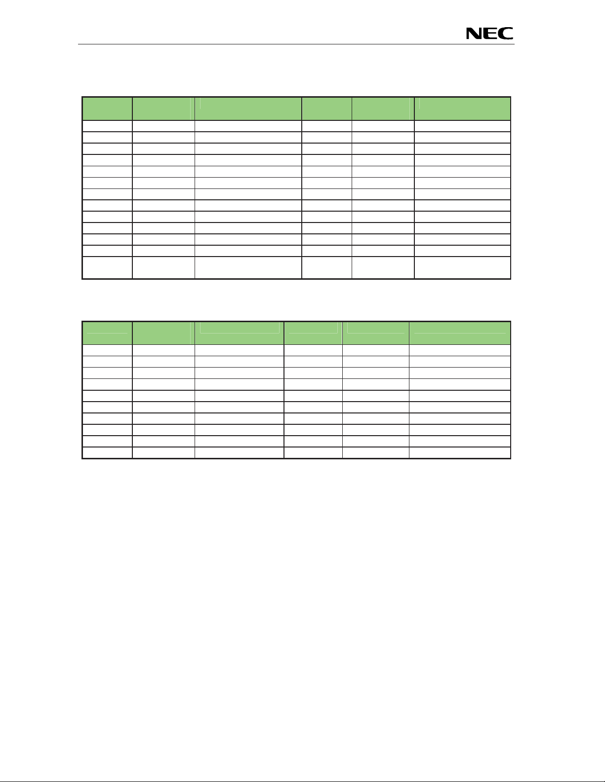
The 7 segment LED U2 is connected to port P90-P97 of the V850ES/HG2 device. A low signal output at
each port switches the corresponding LED on.
Port V850ES/HG2 Segment LED U2
P90 A
P91 B
P92 C
P93 D
P94 E
P95 F
P96 G
P97 DP
Table 12: External LED U2
Example: The figures of 0 to 9 can be displayed by writing the following values to the port register P9.
P9, register
value
0xC0
0xF9
0xA4
0xB0
0x99
LED U2 P9, register
value
0
1
2
3
4
0x92
0x83
0xF8
0x80
0x98
LED U2
5
6
7
8
9
20
Page 21
EB-V850ES/HG2-EE
CN2
CN1
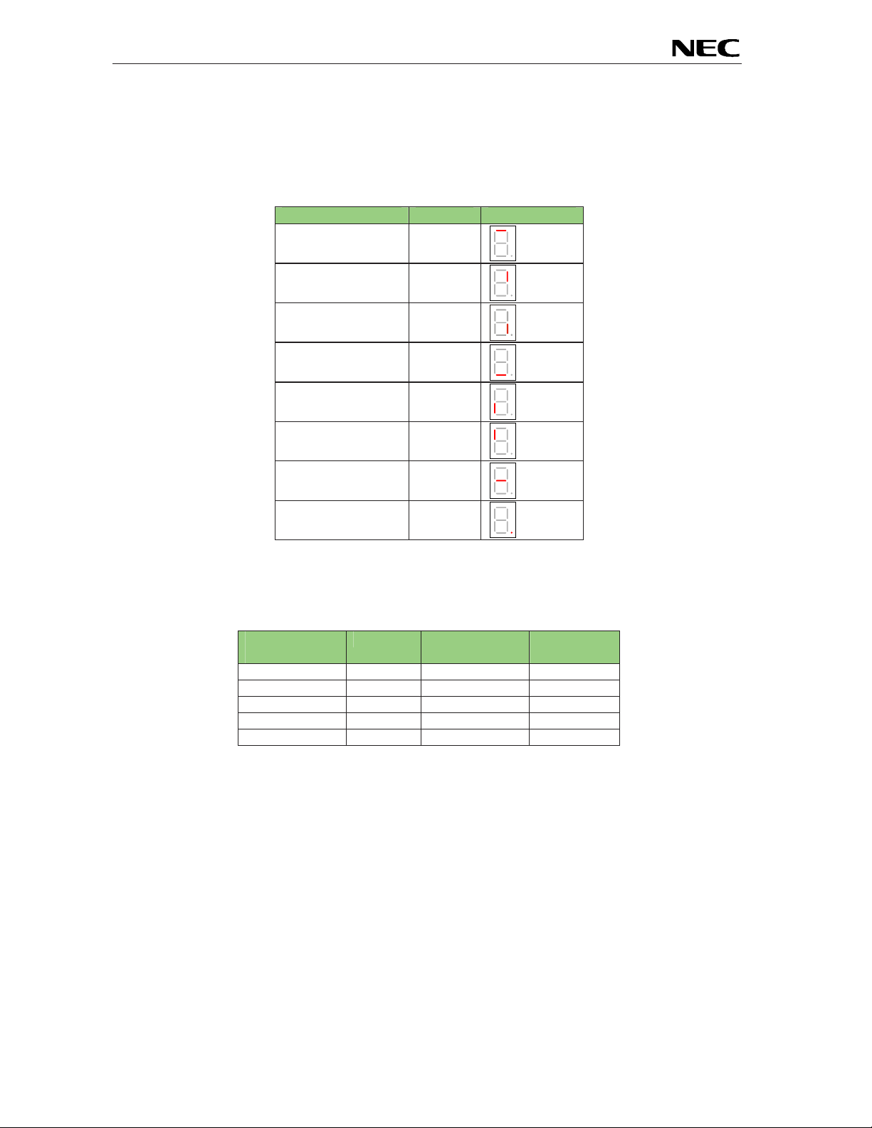
3.11 External connectors CN1 and CN2
CN1 and CN2 are connectors for external user hardware. Please read the user’s manual of the
V850ES/HG2 devic e carefully to get information about the electrical specification of the available I/O
ports.
Figure 5: External connectors CN1 and CN2
21
Page 22

EB-V850ES/HG2-EE
CN1 Signal name V850ES/HG2 Pin name Comment
AVREF0 AVREF0 Connected to VDD by soldering bridge
1
VSS AVSS, VSS, EVSS, BVSS
2
P10 P10/INTP9
3
P11 P11/INTP10
4
EVDD EVDD Connected to VDD by soldering bridge
5
P78 P78/ANI8 Connected to SW3-5 by soldering bridge
6
P79 P79/ANI9 Connected to SW3-6 by soldering bridge
7
FLMD0 FLMD0 Connected to FLMD0 control logic
8
VDD VDD
9
+12V Connected to CN3, J1
10
VSS AVSS, VSS, EVSS, BVSS
11
+12V Connecte d to CN3, J1
12
VDD VDD
13
RESET0 RESET Connected to reset cir c uit
14
VDD VDD
15
+12V Connecte d to CN3, J1
16
P02 P02 / NMI
17
P03 P03 / INTP0 / ADTRG C onnected to SW2
18
P04 P04 / INTP1 Connected to SW1
19
P05 P05 / INTP2 / DRST
20
P06 P06 / INTP3
21
P40 P40 / SIB0
22
P41 P41 / SOB0
23
P42 P42 / SCKB0
24
P30 P30 / TXDA0 Connected to RXD by soldering bridge
25
P31 P31 / RXDA0 / INTP7 Connected to TXD by soldering bridge
26
P32 P32 / ASCKA0 / TOP01 / TIP00 / TOP00
27
P33 P33 / TIP01 / TOP01
28
P34 P34 / TIP10 / TOP10
29
P35 P35 / TIP11 / TOP11
30
P36 P36
31
P37 P37
32
VSS AVSS, VSS, EVSS, BVSS
33
EVDD EVDD Connected to VDD by soldering bridge
34
P38 P38 / TXDA2
35
P39 P39 / RXDA2 / INTP8
36
P50 P50 / KR0 / TIQ01 / TOQ01
37
P51 P51 / KR1 / TIQ02 / TOQ02
38
P52 P52 / KR2 / TIQ03 / TOQ03 / DDI
39
P53 P53 / KR3 / TIQ00 / TOQ00 / DDO
40
P54 P54 / KR4 / DCK
41
P55 P55 / KR5 / DMS
42
P90 P90 / KR6 / TXDA1 Connected to 7seg LED by soldering bridge
43
P91 P91 / KR7 / RXDA1 Connected to 7seg LED by s oldering bridge
44
P92 P92 / TIQ11 / TOQ11 Connected to 7seg LED by solde ring bridge
45
P93 P93 / TIQ12 / TOQ12 Connected to 7seg LED by solde ring bridge
46
P94 P94 / TIQ13 / TOQ13 Connected to 7seg LED by solde ring bridge
47
P95 P95 / TIQ10 / TOQ10 Connected to 7seg LED by solde ring bridge
48
P96 P96 / TIP21 / TOP20 Connected to 7seg LED by solde ring bridge
49
P97 P97 / SIB1 / TIP20 / TOP20 Connected to 7seg LED by solde ring bridge
50
Table 13: Connector CN1
Connected to 4.7 kΩ pull-up resistor
Connected to 4.7 kΩ pull-up resistor
Connected to 4.7 kΩ pull-up resistor
Connected to 4.7 kΩ pull-up resistor
22
Page 23

EB-V850ES/HG2-EE
CN2 Signal name V850ES/HG2 Pin name Comment
P98 P98 / SOB1
1
P99 P99 / SCKB1
2
P910 P910
3
P911 P911
4
P912 P912
5
P913 P913 / INTP4 / PCL
6
P914 P914 / INTP5
7
P915 P915 / INTP6
8
P710 P710 / ANI10 Connected to SW3-7 by soldering bridge
9
P711 P711 / ANI11 Connected to SW3-8 by soldering bridge
10
PCM0 PCM0
11
PCM1 PCM1
12
PCM2 PCM2
13
PCM3 PCM3
14
PCT0 PCT0
15
PCT1 PCT1
16
PCT4 PCT4
17
PCT6 PCT6
18
VSS AVSS, VSS, EVSS, BVSS
19
BVDD BVDD Connected to VDD by soldering bridge
20
PDL0 PDL0
21
PDL1 PDL1
22
PDL2 PDL2
23
PDL3 PDL3
24
PDL4 PDL4
25
PDL5 PDL5 / FLMD1
26
PDL6 PDL6
27
PDL7 PDL7
28
PDL8 PDL8
29
PDL9 PDL9
30
PDL10 PDL10
31
PDL11 PDL11
32
PDL12 PDL12
33
PDL13 PDL13
34
P715 P715 / ANI15
35
P714 P714 / ANI14
36
P713 P713 / ANI13
37
P712 P712 / ANI12
38
PCS0 PCS0
39
PCS1 PCS1
40
P00 P00 / TIP31 / TOP31
41
P01 P01 / TIP30 / TOP30
42
P77 P77 / ANI7
43
P76 P76 / ANI6
44
P75 P75 / ANI5
45
P74 P74 / ANI4
46
P73 P73 / ANI3
47
P72 P72 / ANI2
48
P71 P71 / ANI1
49
P70 P70 / ANI0
50
Table 14: Connector CN2
Connected to 10 kΩ pull-down resistor
23
Page 24
EB-V850ES/HG2-EE
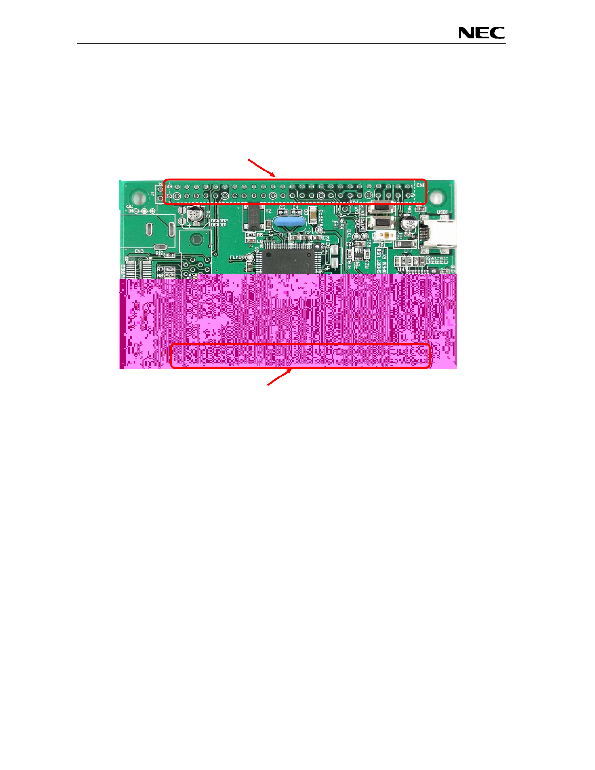
3.12 Soldering Bridges
Some terminals of the V850ES/HG2 device can be customized by opening respectively closing the
corresponding soldering bridge. By opening the soldering bridge the connection to the onboard circuit is
cut. Accordingly, the corresponding signals can be used for external user hardware using the connectors
CN1 and CN2. F o r m o r e de t a i ls plea se r efer t o t h e bo ard schemat i c s, pa ge s 80- 8 1 .
FLMD0
Figure 6: Placement of soldering bridges
Sold e ri n g br idge
name
P90 – P97 Closed
P78 ~ P711 Closed Co nne cted to switch SW3, Bits 5-8
RXD, TXD Closed Connection of ports RXDA0 / P31 and TXDA0 / P30 to the
FLMD0 Open By closing the so lde ring bridge the FLMD0 pin is connected to
AVREF0 Closed Connected to VDD
BVDD Closed Connected to VDD
EVDD Closed Connected to VDD
DCVDD1, DCVDD2 Open When using external power supply, via connector CN3 or J1, the
Factory setting Comment
Connected to 7seg LED via 1 KΩ resistor
FT232 UART/USB circuit.
port pin P37. This allows by using FLASH self-programming to
enable or disable FLASH write operations via port pin P37.
soldering bridges must be closed.
Table 15: Soldering brigdes
24
Page 25
EB-V850ES/HG2-EE
3.13 V850ES/HG2 memory map
The V850ES/HG2 memory layout is shown in the table below.
0x3FFFFFF
SFR Area
0x3FFF000 Free for user application
0x3FFEFFF software
12 KB Internal RAM
0x3FFC000
0x3FFBFFF
Acce ss pro h ibi t e d ar ea
0x3FF0000
0x3FEFFFF Programmable peripheral
I/O area or use prohibited area
Address area
0x0100000 (program fetch prohibited area)
0x00FFFFF
Acce ss pro h ibi t e d ar ea
0x0040000
0x003FFFF
256 KB Flash memory Free for user application
0x0000000 Software
Table 16: V850ES/HG2 memory map
25
Page 26

EB-V850ES/HG2-EE
4. EB-V850ES/HG2-EE installation and operation
4.1 Getting started
The IAR C-SPY debugger allows to download and debug application software on the EB-V850ES/HG2EE starterkit hardware. Additionally the FPL FLASH programming software can be used for simple
FLASH programming of the V850ES/HG2 internal FLASH memory. As communication interface between
the host computer and the EB-V850ES/HG2-EE board a USB interface line is needed. Before you can
download, debug or execute an application programs, hardware and software must be installed properly.
4.1.1 CD-ROM contents
The CD-ROM shows following directory structure:
EB_V850ESHG2_EE (F:)
Acrobat
Doc
FPL
Drivers
FPL
PRM
IAR Embedded Workbench V850
SamplePrograms
Table 17: EB-V850ES/HG2-EE CD-ROM directory structu re
CD-ROM ROO T
- Acrobat Reader for 32Bit Windows OS
- Documentation
- FPL FLASH programming software
… USB driv er
… FPL setup directory
… PRM parameter file
- IAR Embedded Workbench for V850
- Sample program for EB-V850ES/HG2-EE
26
Page 27

EB-V850ES/HG2-EE
5. Hardware installation
After unpacking EB-V850ES/HG2-EE, connect the board to your host computer by using the provided USB
interface cable. When EB-V850ES/HG2-EE is connected, the USB driver needs to be installed on the host
machine. Please refer to the following CHAPTER 6 SOFTWARE INSTALL AT IO N.
6. Software installation
The EB-V850ES/HG2-EE package comes with several software demo packages:
• IAR Systems Embedded Workbench for V850, including C compiler, assembler, linker, librarian
and IAR C-SPY debugger / simulator
• FPL FLASH programming software
• Sample programs
The IAR Systems Embedded Workbench and the FPL FLASH programming GUI must be installed on your
PC. For detailed installation hints, refer to the following chapters and to the corresponding documentation of
the IAR Embedded Workbench.
6.1 IAR Systems Embedded Workbench for V850 installation
To install the IAR Systems Embedded Workbench for V850 including the C-SPY debugger / simulator,
select the SETUP program in the dir ectory \IAR Embedde d Workbench V850\ewv850\ of the CDROM.
The setup dialogues will guide you through the installation process.
6.2 FPL FLASH programming GUI installation
To install the FPL FLASH programming GUI select the SETUP program in the directory \FPL\ of the
CDROM. The setup dialogues will guide you through the installation process.
6.3 Sample program installation
To install the demonstration programs for the EB-V850ES/HG2-EE board select the SETUP pr o g ram i n th e
directory \SampleProgram\ of the CDROM. The setup d ialogues will guide you through the installation
process.
27
Page 28

EB-V850ES/HG2-EE
6.4 USB Driver Installation
When the EB-V850ES/HG2-EE board and FPL is used, the driver needs to be i nstalled on the
host machine. Install the driver according to the following procedure:
Installation on Windows 98SE/Me ......... Page 28
Installation on Windows 2000 ............... Page 30
Installation on Windows XP ............... .... Page 36
6.4.1 Installation on Windows 98SE/Me
1. When the EB-V850ES/HG2-EE board is connected with the host machine, the board is
recognized by Plug and Play, and t he wizard for adding new hardware is started. Cli ck
Next>.
Figure 7: Add New Hardware Wizard (Windows 98SE)
Click.
2. The window below is displayed. So, check that "Search for a suitable driver ..." is selected,
then click Next>.
Figure 8: Search Method (Windows 98 SE)
Check that "Search for a
suitable driver ..." is selected.
Click.
28
Page 29

EB-V850ES/HG2-EE
3. Check the "Specify a location" check box only and enter "C:\Program
Files\NECTools32\FPL\DRIVER" in the address bar, then click Next>.
Figure 9: Search Location Specification (Windows 98SE)
<1> Check "Specify
a l
ocation" only.
備考
<2> Enter "C:\Program Files\NECTools32\FP L\DRIVER".
3.1
ソフトウエアのインスト ール先の フォルダを変更した場合は,
<3> Click.
Remark If the installation destination f older is changed at the time of GUI software installation,
enter "new-folder\DRIVER".
4. The window below is displayed. Click Next>.
Figure 10: Checking Driver to Be Installed (Windows 98SE)
Click.
29
Page 30

EB-V850ES/HG2-EE
5. When the window below is displayed, the installation of the USB driver is completed. Click
Finish. The installation of the USB Serial Port driver is then automatically performed.
Figure 11: Installation Completion (Windows 98SE)
Click.
6.4.2 Installation on Windows 2000
1. When the EB-V850ES/HG2-EE board is connected with the host machine, the board is
recognized by Plug and Play, and t he wizard for finding new hardware is started. Click
Next>.
Figure 12: Found New Hardware Wizard 1 (Windows 2000)
Click.
30
Page 31

EB-V850ES/HG2-EE
that "Search for a
..." is
a
2. The window below is displayed. So, check that "Search for a suitable driver ..." is selected,
then click Next>.
Figure 13: Search Method 1 (Windows 2000)
Check
suitable driver
selected.
Click.
3. Check the "Specify a location" check box only, then click Next>.
Check that "Specify
location" only is checked.
ed.hed.
Figure 14: Driver File Location 1 (Windows 2000)
Click.
31
Page 32

EB-V850ES/HG2-EE
4. Enter "C:\Program Files\NECTools32\FPL\DRIVER" in the address bar, then click OK.
Figure 15: Address Specification 1 (Windows 2000)
Click.
Enter "C:\Program Files\NECTools32\FPL\DRIVER".
Remark If the installation destination folder is changed at the time of GUI software installation,
enter "new-folder\FPL\DRIVER".
5. Click Next>.
Figure 16: Driver File Search 1 (Windows 2000)
Click.
32
Page 33

EB-V850ES/HG2-EE
Click.
6. Click Finish to complete the installation of the USB driver.
Figure 17: USB Driver Installation Completion 1 (Windows 2000)
7. Proceed to the installation of the USB Serial Port driver. Click Next>.
Figure 18: Found New Hardware Wizard 2 (Windows 2000)
Click.
33
Page 34

EB-V850ES/HG2-EE
Check
that "Search for a
..." is
a
suitable driver
selected.
8. The window below is displayed. So, check that "Search for a suitable driver ..." is selected,
then click Next>.
Figure 19: Search Method 2 (Windows 2000)
Click.
9. Check the "Specify a location" check box only, then click Next>.
Check that "Specify
location" only is checked.
Figure 20: Driver File Location 2 (Windows 2000)
Click.
34
Page 35

EB-V850ES/HG2-EE
10. Enter "C:\Program Files\NECTools32\FPL\DRIVER" in the address bar, then click OK.
Figure 21: Address Specification 2 (Windows 2000)
Click.
Enter "C: \Program Files\NECTools32\FPL\DRIVER".
Remark If the installation destination folder is changed at the time of GUI software installation,
enter "new-folder\DRIVER".
11. Click Next>.
Figure 22: Driver File Search 2 (Windows 2000)
Click.
35
Page 36

EB-V850ES/HG2-EE
that "Install from a list
12. Click Finish to complete the installation of the USB driver.
Figure 23: USB Driver Installation Completion 2 (Windows 2000)
Click.
6.4.3 Installation on Windows XP
1. When the EB-V850ES/HG2-EE board is connected with the host machine, the board is
recognized by Plug and Play, and the wizard for f inding new hardware is started. Check
that "Install from a list or specific ..." is selected, then click Next>.
Figure 24: Found New Hardware Wizard 1 (Windows XP)
Check
or specific ..." is selected.
Click.
36
Page 37

EB-V850ES/HG2-EE
best driver in these locations."
2. Check that "Search for the best driver in these locations." is selected. Check t he "Include
this location in the search:" check box and enter "C:\Program
Files\NECTools32\FPL\DRIVER" in the address bar, then click Next>.
Figure 25: Search Location Specification 3 (Windows XP)
<1> Check that "Search for the
is selected.
<2> Check "Include this
location in the search:"
only.
<4> Click. <3> Enter "C:\Program Files\NECTools32\FPL\DRIVER".
3. As shown below, "has not passed Windows Logo testing to v erify its compatibility with
Windows XP." is displayed. Click Continue Anyway.
Figure 26: Window s XP Logo Testi ng 3 (Wind ows XP)
Click.
37
Page 38

EB-V850ES/HG2-EE
that "Install from a list
4. When the window below is displayed, the installation of the USB driver is completed. Click
Finish .
Figure 27: USB Driver Installation Completion 1 (Windows XP)
Click.
5. Proceed to the installation of the USB Serial Port driver. Click Next>.
Figure 28: Found New Hardware Wizard 2 (Windows XP)
Check
or specific ..." is selected.
Click.
38
Page 39

EB-V850ES/HG2-EE
that "Search for the best
<2> Check
"Include this location
6. Check that "Search for the best driver in these locations." is select ed. Check the "Include
this location in the search:" check box and enter "C:\Program
Files\NECTools32\FPL\DRIVER", then click Next>.
Figure 29: Search Location Specification 2 (Windows XP)
<1> Check
driver in these locations." is
selected.
in the search:" only.
<3> Enter "C:\Program Files\NECTools32\FPL\DRIVER".
<4> Click.
7. As shown below, "has not passed Windows Logo testing to v erify its compatibility with
Windows XP." is displayed. Click Continue Anyway.
Figure 30: Window s XP Logo Testi ng 2 (Wind ows XP)
Click.
39
Page 40

EB-V850ES/HG2-EE
8. When the window below is displayed, the installation of the USB driver is completed. Click
Finish .
Figure 31: USB Serial Port2 Driver Installation Completion (Windows XP)
Click.
40
Page 41

EB-V850ES/HG2-EE
Check
that "USB Serial Port
6.5 Conf i rm ati on of USB Dri ver In sta ll at io n
After installing the two types of drivers, check that the drivers have been instal led normally,
according to the pr ocedure below. W hen using the EB-V850ES/HG2-EE board i n co m bi nat i on
with FPL GUI, the information to be checked here is needed.
By clicking the "Device Manager" tab, check that the drivers are installed normally.
Figure 32: Device Manager
(COM?)" is present.
Check that "USB High Speed
Serial Converter" is present.
For Windows 98SE/Me
Caution Do not select Update and Erase when communicating with the target
device.
For Windows 2000/XP
Caution Do not perform "Hardware Modification Scan" when communicating with the
target device.
Remark In the GUI port l ist box, the same communication port as COM? of USB Serial Port
(COM?) needs to be selected.
If the drivers above are not displayed, or the mark "×" or "!" is prefix ed, refer to
CHAPTER 9 TROU BLESHOOTING.
41
Page 42

EB-V850ES/HG2-EE
6.6 Driver Uninstallation
The driv er uninstallati on program is installed on the host machine when the F PL software is
instal l e d. U se t h e pr o c ed ur e be low f or driver uninst alla t ion.
1. When using Windows XP, log on as the computer administrator. When using Windows
2000, l o g on as th e A dmi nistr a t or .
2. Double-click in the order from "My Computer" to "(C:)" to "Program Fi les" to "NECTools32"
to "FPL" t o " DR IVER" . "Ftd i u nin. exe" is displa y ed . Do ub l e - c l ick "Ftdi u n i n . exe" .
Figure 33: Driver Uninstallation
Double-click.
3. Click Continue.
Figure 34: Driver Uninstaller
Click.
42
Page 43

EB-V850ES/HG2-EE
Click.
4. Click Finish to complete driver uninstallation.
Figure 35: Completion of Driver Uninstallation
Caution If the GUI software is uninstalled earlier, "Ftdiunin.exe" is also deleted. At this time,
delet e "USB Serial Port (COM?)" and "USB High Speed Serial Converter" from Device
Manager manually.
43
Page 44

EB-V850ES/HG2-EE
Programm er
window
7. FPL FLASH programming software
7.1 Introduction
The parameter file of t he V850ES/HG2 device is installed automatically during installation of FPL
GUI, folder <FPL install-path>\PRM. Nevertheless, newest version of parameter file for the
µPD70F3707 device can by download from the NEC Electronics Web site.
Download the parameter file for the PG-FP4 from the following NEC Electronics Web site:
Copy the parameter file downloaded from the NEC Electronics Web site into sub-directory
<FPL.EXE-install-path>\PRM created during GUI software setup (refer to CHAPTER 6
SOFTWARE INSTALLATION).
7.2 Starting up the GUI Software
• GUI software startup
Select FPL.EXE from the start menu to start the FPL GUI software.
When the GUI software is started normally, the following screen appears.
Menu bar
http://www.eu.necel.com/updates
Figure 36: GUI Software Main Window
Toolbar
Status bar
parameter
Action log window
44
Page 45

EB-V850ES/HG2-EE
Thi s wi nd ow co nsi s ts of t h e fol l o win g i t ems:
Name Display Information
Menu bar
(displayed at the top)
Toolbar
(displayed under the menu bar)
Action log window
(displayed under the toolbar)
Programmer parameter window
(displayed to the right of the action log
window)
Status bar Displays status.
7.3 Toolbar
The toolbar contains buttons for starting the important procedures of the FPL.
Figure 37: Toolbar Buttons
Displays menu items executable by the
FPL.
Displays frequently used commands as
icons.
Displays an FPL action log.
Displays programming parameter
settings.
evice] → [Setup] button
[D
ile] → [Load] button
[F
evice] → [Bla nk Ch eck ] but to n
[D
evice] → [Erase] button
[D
evice] → [Program] button
[D
evice] → [Verify] button
[D
evice] → [Autoprocedure(EPV)] button
[D
45
Page 46

EB-V850ES/HG2-EE
7.4 Menu Bar
Depending on the actual device status and dev i ce type, some menu items may be enabled or
disabled.
7.4.1 [File] menu
Clicking the [F
This menu mainly contains commands related to file operation.
ile] menu displays the pull-down menu as shown below.
Figure 38: [File] Menu
(1) [L
oad] command
The [L
oad] comm a nd al lows you t o sel ec t a pr o g r am f i le.
The selected program file is programmed into the flash memory of the dev ice by
executing the [P
rogram] command or [Autoprocedure(EPV)] command.
Figure 39: HEX File Sel e ct ion Window
T he f il e sel ect ion wind ow fo r pr ogram l oadi ng di spla ys t he m ost rece ntl y u sed di re ctor y t o
which a user program has been loaded. After a user program is loaded, a checksum
calculation is made and the result is displayed in the programmer parameter window.
[ O
pen button]
Selects a user program as a program to be written to the target device.
[ Cancel button]
Closes the window without selecting a program.
46
Page 47

EB-V850ES/HG2-EE
(2) [Q
The [Q
User settings are sav ed in the F PL.INI
uit] command
uit] menu is the command for terminating the FPL GUI software. Clicking × on the
right side of the task bar also terminates the FPL GUI software.
Note
file, so that the GUI software starts up next time
with the same settings.
Note FPL.INI is created in the Windows folder when Windows 98SE, Windows Me, or
Windows XP is used.
When Windows 2000 is used, FPL.INI is created in the Winnt folder.
7.4.2 [D
evice] menu
Clicking the [D
evice] menu displays the pull-down menu as shown below.
This menu mainly contains commands for programming operations such as deletion,
programming, and verification on the target device.
(1) [B
lank Check] command
The [Blank Check] comm and allows you to make a blank check on the target device
connected to the F PL. If the flash memory of t he target device is erased, a blank
check is terminated normally. If the flash memory is not completely erased, the
indication "not blank" is provided. Before starting programming, erase the flash
memory of the target device.
(2) [E
rase] command
The [E
rase] command erases the f lash mem ory of the target device c onnected to the
FPL. W hi l e the fl ash me mo ry i s bein g era sed, th e pr ogre ss st at us i s di spl ay ed i n the
action log window to indicate programmer operation.
The execution on the [B
executed follows the setti ng of 'Command options' of the Advance tab displayed by
selecting [D
evice] → [Setup].
Upon completion of [E
of executing the command on the target device.
Figure 40: [Device] Menu
lank Check] command before the [Erase] command is
rase] command execution, the GUI software displays the result
47
Page 48

EB-V850ES/HG2-EE
(3) [Program] command
The [P
rogram] command sends a specified user program to the target device and
writes the program to the fl ash memory.
The execution of Verify operation for detecting an error in user program
communication from the FPL to the target device after the execution of t he [P
command follows the setting of the 'Comm and options' on the Advance tab displayed
by selecting [D
During programming, the progress status is displayed in the action log window to
indicate programmer operation. This progress status display window displays the
progress status on target device programming by percentage.
Upon completion of [P
result of executing the command on the target device.
(4) [V
(5) [S
This command is not supported.
(6) [Checksum
The [Checksum
This value differs from the value displayed in the parameter window of the main window.
(7) [A
(8) [Sig
The [Sig
erify] command
The [V
erify] command sends a speci f ied user program to the target device connected
with the FPL, and perf orms verifi cation agai nst the data written to the flash memory
of the target device.
During verification, the progress status is displayed in the action log window to
indicate programmer operation. This progress status display window displays the
progress status of target device verification by percentage.
Upon completion of [V
of executing the command on the target device.
ecurity] command
] command
the FPL.
utoprocedure(EPV)] command
The [A
command and [V
When a user program is to be resent to the target device for comparison with the data
written to the flash memory of the target device because of a user program
communication error, execute the [P
[S
execution of the [V
During EPV execution, the progress status is displ ayed in the action log window to
indicate programmer operation. For a selected command, its execution operation,
and messages, refer to CHAPTER 8 HOW TO USE FPL.
Upon completion of [A
displays the result of executing the command on the target device.
nature read] command
memor y i n for m a t ion, an d so fort h) of th e t a r ge t .
utoprocedure(EPV)] command executes the [Erase] command, [Program]
etup] and specifying 'Command options' on the Advance tab, then set the automatic
nature read] command reads the signature information (device name, flash
evice] → [Setup].
rogram] command execution, the GUI software displays the
erify] command execution, the GUI software displays the result
] command reads the checksum value of the target devi ce connected with
erify] command in succession.
rogram] command by selecting [Device] →
erify] command.
utoprocedure(EPV)] command execution, the GUI software
rogram]
48
Page 49

EB-V850ES/HG2-EE
(9) [Setup] command
The [S
according to the user environment and to set command options. Each time the GUI
software is started, the most recently used parameter file (.PRM) is read and the
settings are di splayed. The [S
other than those items consisting of shadowed characters according to the user
environment.
(a) Standard setup
This menu is used to set the environment for rewriting the flash memory of the target
device.
The mode of communication with the target, the operating clock, and so forth differ
depending on the device used. For details, refer t o the manual of the device used,
when making settings.
The window shown below is opened.
etup] menu allows you to make settings related to flash memory rewriting
etup] menu allows you to modify the settings of items
Figure 41: Device Setup Window - Standard
This window shows all basic options that can be set in accordance with the user
environment and target device.
[ OK button]
Clicking the OK button saves the settings on the Standard and Advance menus and
closes the window.
[ Cancel button]
Clicking the Cancel button closes the window without saving the settings on the
Standard and Advance menus.
49
Page 50

EB-V850ES/HG2-EE
<1> Parameter file
This file holds parameters and timing data required to rewrite the flash memory of
the target device. Do not modify the data in the param eter fil e because the data is
related to the guarantee of rewrite data.
The parameter file is protected by the checksum function. If the checksum result
indicates an error, the FPL does not accept the parameter file.
Figure 42: Setup Window - Pa ram e ter File Sel ec tion
Figure 43: Parameter File Selection Window
[ PRM File Read button]
A window for specifying a parameter file is displayed. Specify a desired file then
pen.
click O
50
Page 51

EB-V850ES/HG2-EE
<2> Communication interface to device
"Com m uni cat ion inte rf ace t o dev i ce" i s use d to se lec t a ch anne l f or c om mu nic ati on
between the EB-V850ES/HG2-EE board and host machine.
Figure 44: Setup Window - Communication interface to device
[Port list box]
Select a channel for communication between the EB-V850ES/HG2-EE board and
host machine.
• COM1 to COM16
Remark Selectable ports can be checked using Device Manager. For details,
refer to CHAPTER 6.5 Confirmation of USB Driver Installation.
[Speed list box]
Select a communication rate for the selected communication channel from the
following:
• 9600 bps
• 19200 bps
• 38400 bps
Remark For selectable communication rates, refer to the user's manual of the
device used.
<3> Supply oscillator
"Supply oscillator" is used to select a clock that determines programming, data
transfer, and a transfer rate.
51
Page 52

EB-V850ES/HG2-EE
<4> Operation Mode
The setting of "Operation Mode" may divide the flash memory of some target
devices into blocks or areas.
This menu is used to select an operation mode of the flash memory. Som e dev ices
do not have the block and area divi sion modes, and some devi ces have only one of
the modes. In these cases, a nonexisting mode is unchoosable.
Figure 46: Setup Window - Operation Mode
[When Chip is selected]
The entire flash memory area of the target device is subject to rewrite processing.
[When Block is selected]
Specify the Block number range subject to rewrite processing by using Start/End.
The Start/End list box es display the Block numbers where the flash memory of the
target device is configured.
[When Area is selected]
Specify the Area number range subject to rewrite processing by using Start/End.
The Start/End list boxes display the Area numbers where the flash memory of the
target device is configured.
[Show Address check box]
Specify whether numbers or addresses are displayed in the Start/End list boxes.
If this check box is checked, addresses are displayed.
If this check box is not checked, numbers are displayed.
52
Page 53

EB-V850ES/HG2-EE
(b) Advance setup
The Advance setup menu is used to specify the command options and security flag
settings.
When "Advance" is clicked, the following window is displayed:
Figure 47: Device Setup Window - Advance
<1> Command options
This dialog box is used to specify the FPL flash processing command options.
Figure 48: Setup Window - Command options
[Blank check before Erase check box]
If this check box is checked, blank check is made before the Erase command or
EPV command is executed.
If the result of a blank check indicates OK, erase processing is not executed.
[Read verify after Program check box]
If this check box is checked, write data is sent from the programmer after execution
of the Program command and EPV command, then the data is v erif ied against the
data written to the fl ash memory.
[Security flag after Program check box] Not usable
[Checksum after Program check box]
If this check box is checked, the flash memory checksum v alue of the target devi ce
is read from the target device after execution of the Program command and EPV
command.
This v alue dif fers from the val ue displayed i n the parameter window of the main
window.
<2> Security flag settings Not usable
53
Page 54

EB-V850ES/HG2-EE
7.4.3 [V
iew] menu
Clicking the [V
iew] menu displays the pull-down menu shown below.
This menu contains commands for setting whether to display the toolbar and status bar.
Figure 49: [View] Menu
(1) [Toolbar] command
Checking the [T
oolbar] command displays the toolbar. Unchecking the command hides
the toolbar.
(2) [S
Checking the [S
tatus Bar] command
tatus Bar] command displays the status bar. Unchecking the command
hides the status bar.
54
Page 55

EB-V850ES/HG2-EE
7.4.4 [H
elp] menu
Clicking the [H
elp] menu displays the following pull-down menu:
Figure 50: [Help] Menu
(1) [About FPL] command
The [A
bout FPL] command opens the program entry window as shown bel ow and indicates
the version.
Clicking OK terminates the display.
Figure 51: About FP L Wind ow
55
Page 56

EB-V850ES/HG2-EE
7.5 Programm er Parameter Wind ow
This window displays the settings of the programming parameters.
Figure 52: Programmer P ara m eter Window
[Device]
Updated after communication with the target device to display information about the target
device.
[Parameter file]
Updated af t er [S
etup] command execution to display information about a read parameter file.
[Loa d file]
Updated af t er [L
oad] command execution to select information about a selected program file.
[Connection to device]
Updated af t er [S
etup] command execution to display information about the connection with the
target device.
56
Page 57

EB-V850ES/HG2-EE
8. How to use FPL FLASH programming software
This chapter explains the basic operations of the FPL GUI for programming the EB-V850ES/HG2-EE
board. This chapter covers how to start the system, execute the EPV command, and program the target
V850ES/HG2 device.
The conditions of the series of operations described in this chapter are as follows:
Hardware configuration of EB-V850ES/HG2-EE:
Board : EB-V850ES/HG2-EE
CPU : V850ES/HG2
Target device : µPD70F3707
Clock : 5 MHz
Voltage level : 5 V
Software configuration of FPL:
Parameter fil e: 70F3707.PRM
Clock setting : 5 MHz Multiplied by 4
Port : COM3 (38400 bps)
Operation mode: Chip
Write HEX : CountDownTimer.hex
Option setting : Blank check before Erase
(1) Installing the FPL GUI software
Install the FPL GUI software on the host machine you are using, by referring to CHAPTER 6
SOFTWARE INSTALLATION (if the software has not been installed yet).
(2) Installing the driver
Install the USB driver on the host machine you are using, by referring to CHAPTER 6
SOFTWARE INSTALLATION (if the driver has not been installed yet).
(3) Installing the parameter file
The parameter file f or the V850ES/HG2 device is installed automatically during installation of FPL
GUI, folder <FPL install-path>\PRM. Nevertheless, newest version of parameter file for the
µPD70F3707 device can by download from the NEC Electronics Web site.
Download the parameter file for the PG-FP4 from the following NEC Electronics Web site:
Copy the parameter file downloaded from the NEC Electronics Web site into sub-directory
<FPL.EXE-install-path>\PRM created during GUI software setup (refer to CHAPTER 6
SOFTWARE INSTALLATION)..
http://www.eu.necel.com/updates
57
Page 58

EB-V850ES/HG2-EE
(4) Connecting and starting
<1> Set the EB-V850ES/HG2-EE board to the FLASH programming mode by configuring SW3
as following:
<2> <Plug and Play> Connect the E B-V850ES/HG2-EE board with the host machine via the USB
cable. If the connection was already done, press the reset button SW4 t o release the FLASH
programming mode.
SW3 Configuration
Bit 1 ON
Bit 2 OFF
Bit 3 ON
Bit 4 ON
58
Page 59

EB-V850ES/HG2-EE
<3> Start the FPL GUI.
Figure 53: GUI Software Startup Screen
(5) Setting the programming environment
<1> Select [D
evice] → [Setup] from the menu bar.
<2> The Standard dialog box for device setup is activated.
Figure 54: <Standa rd De vice Se tup> D ialog Box
59
Page 60

EB-V850ES/HG2-EE
<3> Click PRM File Read to open the parameter file selection window.
Select the parameter file “70F3707.prm” then click Open.
Figure 55: Parameter File Selection
<4> From the Port list box, select the communication port that matches the host machine being
used. Select the communication speed of the Host connection.
Figure 56: Port Selection
Remark Selectable ports can be checked using Device Manager. For details, refer to
CHAPTER 6.5 Confirmation of USB Driver Installation.
60
Page 61

EB-V850ES/HG2-EE
<5> Set "Supply oscillator" according to the specifications of the EB-V850ES/HG2-EE board,
“Frequency = 5.00 MHz” and “Multiply rate = 4.00”. In "Operation Mode", please
specify the “Chip” mode. The following figure shows the recommended settings:
Figure 57: <Standa rd De vice Se tup> D ialog Box after Setting
<6> Switch to the Advance dialog box.
Figure 58: <Advance Device Setup> Dialog Box
<Command options>
Blank check before Erase : Checked
61
Page 62

EB-V850ES/HG2-EE
displayed
.
<7> Click the OK button. The GUI software sets the parameters.
When the settings have been com pleted, the foll owing screen is displayed:
Figure 59: Completion of Parameter Setting
"PRM File Read OK." is displayed.
The display is updated.
(6) Selecting a user program
<1> Select [F
ile] → [Load].
<2> Select a program file to be written to the target device, then cl ick O
Figure 60: After Downloading
"Success read HEX file." is
pen.
The display is updated.
62
Page 63

EB-V850ES/HG2-EE
(7) [Autoprocedure(EPV)] command execution
Select [D
When the [Autoprocedure(EPV)] command is executed, Blank Check → Erase → Program and
FLASH Internal Verify are executed sequentially for the µPD70F3707 device.
evice] → [Autoprocedure(EPV)] from the menu bar.
Figure 61: After EPV Execution
"...finish" is displayed.
(8) Terminating the GUI
Select [F
ile] → [Quit] to terminate the GUI software. All settings executed so far are saved in the
FPL.INI file, so that those settings can be reused when the GUI software is restarted.
(9) Execute “CountDownTimer” application
Set the EB-V850ES/HG2-EE board to the normal operation mode by switching SW3, Bits 1-4, to
OFF. < Plug and Play> the EB-V850ES/HG2-EE board to start in normal operation mode or press
the reset button SW4 to release the normal operation mode.
(10) Restarting the GUI
When the system is restarted, the same screen as shown in Figure 59 appears.
63
Page 64

EB-V850ES/HG2-EE
9. TROUBLESHOOTING
In driver installation, recognition based on Plug and Play is disabled.
Cause:
The USB connector may not be inserted normally into the USB port of the personal computer.
Action:
Check that the USB connector is inserted fully into the USB port of the personal computer.
Alternatively, disconnect the USB connector, then insert the USB connector again after a while.
The driver file cannot be found at a specified location.
Cause:
The FPL FLASH programming software may not be installed correctly.
Action:
Install the GUI software again by referring to CHAP T ER 6 Software Installation.
In checking by Device Manager, "USB Serial Port" or "USB High Speed Seria l
Converter" is not displayed. Alternatively, the "!" or "×" is prefixed.
Cause:
The USB connector may not be inserted normally into the USB port of the personal computer.
Action:
Check that the USB connector is inserted fully i nto the USB port of the personal computer.
Alternatively, disconnect the USB connector from the USB port, then insert the USB connector
again after a while.
Cause:
The driver may not be installed correctly.
Action:
<1> When thi s product is connected to the personal computer, right-click the driver marked
with "!" or "×".
Click E
<2> On Device Manager, execute [Hardware Modification Scan].
<3> Install the driver again with Plug and Play.
Cause:
The device may not be recognized (in the case of connection with the USB hub).
Action:
Try the following:
• Disconnect the USB connector, then insert the USB connector again.
• Connect the USB connector to another port of the USB hub.
If the same symptom occurs, do not use the USB hub, but directly connect the c onnector to
the USB port of the personal computer.
When this product is connected with a personal computer, the "Add New Hardware
Wizard" screen is displayed.
Cause:
If the USB connector of this product is not inserted into the USB port used at the installation
time but into another USB port, this product may be recognized as a new hardware item.
Action:
Install the driver by referring to CHAPT ER 6.4 USB Driver Ins tall ation.
rase when displayed.
64
Page 65

EB-V850ES/HG2-EE
Communication with the EB-V850ES/HG2-EE board is disabled.
Cause:
The driver may not be installed correctly.
Action:
Check if "U SB Ser ial Po rt" and "USB H igh Spee d Seri al Co nve rter " are i nstal led c orrect ly by
referring to CHAPTER 6.4 USB Driv er Instal la tion.
Cause:
The COM port selected via the “Port list box” within devi ce setup menu of FPL may not be set
correctly.
Action:
Set the port checked using Device Manager.
Cause:
The EB-V850ES/HG2-EE board is operating in normal or debugging mode.
Action:
Set the board to the FLASH programming mode.
Cause:
The PRM file selected in [Device Setup] may be incorrect.
Action:
Use the corresponding PRM file that matches the target device. For information about the
PRM file, ref er to CHAPTER 7 FPL FLASH programming software.
Cause:
The setting of "Supply oscillator" in [Device Setup] may be incorrect.
Action:
Make a correc t setting according to the specifications of the target devic e.
65
Page 66

EB-V850ES/HG2-EE
10. On-Board debugging
Before using the On-Board debug function of the EB-V850ES/HG2-EE board together with the IAR C-SPY
debugger i t is necessary to install the USB driver f irst. The EB-V850ES/HG2-EE starterkit uses a monitor
program for debugging purpose. The communication between the starterkit and the IAR C-SPY debugger that is running on the personal computer - is done via the standard UART / USB connection. The monitor
program is automatically downloaded to the starterkit in that case when the V850ES/HG2 internal FLASH
memory was erased by the user i.e. by using the FPL. Therefore the user has not to take care about the
monitor.
For communication interface the build-in UARTA0 of the V850ES/HG2 device is used by the monitor.
Consequently it can not be used by the user application.
To set the EB-V850ES/HG2-EE starterkit to the On-Board debug mode configure SW3 as following:
SW3 Configuration
Bit 1 ON
Bit 2 ON
Bit 3 ON
Bit 4 OFF
66
Page 67

EB-V850ES/HG2-EE
10.1 Monitor resources
The debugging feature of the EB-V850ES/HG2-EE starterkit has been realized by a monitor program that is
running on the V850ES/HG2 device. Therefore, the following resources are reserved by monitor and can
not be used by a user program.
10.1.1 UARTA0
The UARTA0 of the V850ES/HG2 device is reserved for the monitor program and can not be used by a user
program.
Device UART for
Debugging
V850ES/HG2
(µPD70F3707)
Additionally, please note the following points:
• Do not change the control registers of UARTA0.
• Do not change or disable the interrupt control / mask flags of UARTA0.
• Do not change the port mode or port mode control registers for port bits P30 and P31.
• Debugging functions like forcible break (debugger stop command) do not operate normally in the
following states where the clock supply to UARTA0 is disabled:
IDLE mode
STOP mode
Main oscillation (fx) is stopped.
UARTA0 UA0RMK P30 / TXDA0
Interrupt
control flag
Terminal used
P31 / RXDA0
10.1.2 Interrupt vectors
The following interrupt vectors are used by the monitor program and can not be used by a user program.
Device Interrupt vector
address
0x0060 – 0x 0063 DBTRAP debug interrupt vector V850ES/HG2
(µPD70F3707)
0x0270 – 0x0273 UARTA0 receive interrupt vector
Function
67
Page 68

EB-V850ES/HG2-EE
10.1.3 Reset vector
When a user program is downloaded by using the IAR C-SPY debugger, the reset vector (address 0x0000)
of the user program is replaced by the one of monitor program. The debugger moves the reset vector of the
user program automatically to address 0x0004. The correction of the relative jump address is also done
automatically by the debugger.
Example:
0x0000
0x0006
0x0008
10.1.4 Memory area
The monitor program is located in the highest FLASH block of the V850ES/HG2 device. Only 2 kByte of
memory are allocated by the monitor program.
Device Address range Function
V850ES/HG2
(µPD70F3707)
Moreover, the monitor reserves 36 bytes of the global stack area by halting the user program, caused by a
forcible break (debugger stop c omm and) or a software breakpoint.
10.1.5 Clock operation
After releasing a reset, the monitor program sets the operation clock of the CPU to the maximum speed of
20 MHz. The monitor program switches also to the maximum CPU speed of 20 MHz when releasing a
forcible break (debugger stop command) or when the user program execution is stopped caused by a
software breakpoint. After the user program execution is restarted (debugger go command) the monitor
restores the previous CPU operation clock setting.
Note: Do not change the frequency of the external oscillator connected to the X1 and X2 pins.
The ba ud ra t e ca l cul atio n for UA R T A0 i s ba sed on a 5 MH z input fre qu en c y, oth er wise no
communication to the EB-V850ES/HG2-EE starterkit can be established.
MOV _start, R31
JMP R31
0x0003F800 - 0x0003FFFF Reserved for monit or
0x0000
0x0004
0x000A
JR monitor
MOV _start, R31
JMP R31
program
10.1.6 Other limitations
The watchdog timer 1 and 2 can not be used. Please be sure to set the option bytes of the V850ES/HG2
device accordingly to allow the watchdog timer disable.
The forcible break (debugger st op command) can not be used when the global interrupts were disabled by
the user program (DI instruction).
68
Page 69

EB-V850ES/HG2-EE
10.2 IAR sample session
When everything is set up correctly the IAR Embedded W orkbench can be started. To do so, start the
Embedded Workbench from Windows “Start” menu > “Programs” > f older “IAR Systems” > “IA R Embedded
Workbench Kickstart for V850”. The following screen appears:
Figure 62: IAR Embedded Workbench
Now select the option “Open exiting workspace” from the “File” menu and locate the sample project. Open
the file “EB_V850ESHG2_EE.eww”. This is the workspace file that contains general information about the
demonstration projects and settings.
69
Page 70

EB-V850ES/HG2-EE
After the demo workspace has been opened the projects contained in the workspace are displayed. Now
click on the little “+” sign next to the “Reac tion Tim e” project to show files that were part of the project. The
screen should now look similar to this:
Figure 63: IAR project workspace
As a next step check some settings of the IAR Embedded Workbench that have to be made for correct
operation and usage of the On-Board debug function of the EB-V850ES/HG2-EE board. First highlight the
upper folder called “Reaction Time – Debug” in the workspace window. Then select “Project” > “ Options”
from the pull-down menus. Next select the category “Debugger”. Make sure that the driver is set to “T KV850” in order to use the On-Board debug function of the EB-V850ES/HG2-EE board. The device
description file must be set to “io70f3707.ddf” according to the V850ES/HG2 device.
Select “TK-V850”
to use On-Board
debugging.
Choose device
description file
io70f3707.ddf
Figure 64: IAR debugger options 1/2
70
Page 71

EB-V850ES/HG2-EE
Choose
serial port
Before using the On-Board debug function it is necessary to set the corresponding USB serial COM port of
the host computer. To set the COM port, please select the category “TK-V850” and choose the
corresponding serial port.
Figure 65: IAR debugger options 2/2
Next the correct linker settings of the demo project will be checked. This can be done in the “Linker”
category as shown below. Select the “Config” tab and check that the linker command file “DF3707.XCL” is
selected. This file is used by the linker and contains information on where to place the diff erent sections of
code and data that may be used within the demo project:
Figure 66: IAR Linker options
71
Page 72

EB-V850ES/HG2-EE
Now after everything has been setup correctly it’s time to compile and link the demonstration project. Close
the Options menu and select “Rebuild All” from the “Project” menu. If the project is compiled and linked
without errors or warnings it can now be downloaded to the EB-V850ES/HG2-EE board and debugged.
To start the IAR C-SPY debugger select the option “Debug” from the “Project” menu or press the (
“Debugger” button. In the next step the TK-V850 Emulator has to be configured before downloading a new
application. Press the OK button to enter the hardware setup menu. Set the configuration as show in the
figure below and start the download by pressing the OK button.
)
Figure 67: TK-V850 hardware setup menu
72
Page 73

EB-V850ES/HG2-EE
Now the de b ug ger i s sta r t ed an d t h e de mo pro j e c t is downlo ad e d t o th e EB-V850ES/HG2-EE board. In ot her
words, the FLASH memory of the V850ES/HG2 device is reprogrammed wi th the user application. The
progress of downloading is indicated by blue dots in the TK-V850 Emulator window.
Figure 68: IAR project download
73
Page 74

EB-V850ES/HG2-EE
After the download was completed all debug features of IAR C-SPY debugger are available, i.e. Single
Stepping (Step Over/-In/-Out), Go, Stop, Breakpoints, Register / Memory view etc.
To get more details on the debugger configuration and capabi lities please refer to the “V850 IAR Embedded
Workbench IDE User Guide” of the IAR installation.
Figure 69: IAR C-SPY debugger
74
Page 75

EB-V850ES/HG2-EE
11. Sample programs
11.1 General Introduction
Each of the sample programs is located in a single directory, which will be called main-directory of the
sample. This main directory of each sample contains the complete project inclusive all output files of the
development tool. The workspace file “EB_V850ESHG2_EE.eww” is located on top of the sample program
directories. All sample programs use the same directory structure:
Count Down Timer
Debug
inc
Release
settings
source
xcl
CountDownTimer.dep
CountDownTimer.ewd
CountDownTimer.ewp
Electronic Dice
Entrance Code Checker
Lightshow
Melody Maker
Reaction Time Measurement
EB_V850ESHG2_EE.eww
Table 18: Example directory structure
The main directory contains only the project files for the IAR Systems Embedded Workbench. All source
files are located in the directory /source and th e /inc directory contains the header files. The /xcl
directory contains the linker control file of the V850ES/HG2 device. Each sample project uses two targets.
One target is the “Debug” (directory /Debug) that holds all information for debugging purpose and the other
one the “Release” target (directory /Release) contains the programmable file, i.e. the Intel HEX file, for
prog ramming the V850ES/HG2 internal FLASH memory by using the FPL soft ware.
All output files of the development tools for the corresponding target are generated in the directories
/Debug and /Release.
For details of using the IAR Embedded Workbench and the IAR C-SPY debugger please refer to the “V850
IAR Embedded Workbench IDE User Guide”.
V850ES/HG2 project and output files
debug output files for IAR C-SPY debugger
C header files
release output files, i.e. Intel HEX file
configuration files, IAR Embedded W orkbench
C source files
Linker control file
dependency information file, IAR Embedded Workbench
project setti ng fi le, IAR C-SPY debugger
project file, IAR Embedded Workbench
V850ES/HG2 project and output files
V850ES/HG2 project and output files
V850ES/HG2 project and output files
V850ES/HG2 project and output files
V850ES/HG2 project and output files
workspace file, IAR Embedded Workbench V850
75
Page 76

EB-V850ES/HG2-EE
11.2 Count Down Timer
With this sample program the board can be used as a count down timer. After the signal for program start
the program waits for the input of the counter time, which can be set by key SW2. Each key press increases
the time by 60 seconds. The current time is shown by the 7 segment LED in units of minutes. A press of
button SW1 starts the timer, which is shown by the flashing dot of the 7 segment LED.
After the selected time is finished, the 7 segment LED flashes for 3 minutes. Then the program goes to
stand by modus. A key press during countdown time or st and-by-modus s ets the program to input mode
again.
Timer P1 is working in the modus ‘clear and start on match between Timer P1 (TMP1) and TP1CCR0’.
According to the selected operating frequency and the value of the compare register TP1CCR0 Timer P1
gener at e s a 25 ms ti m e b ase .
Used I n tern al Peri pher als Used External Parts Source Modules
Timer P1 (TMP1) LED U2 timer.c Main function
Button SW1 init.c Hardware and bit initialization
Button SW2 interrupt.c interrupt functions
rsu . s85 ID cod e an d op t ion by t e se t tin g
11.3 Electronic Dice
This sample program simulates a dice. After the program-start-signal, the program waits for a press of
button SW1. After an animation of a rolling dice a random number between one and six is generated and
shown on the 7 segment LED.
The ‘random’ number is generated by a transformation of the timer value of Timer P2 to a number between
one and six. Timer P2 is working at 2.5 MHz using a compare value of 80 in the modus ‘clear and start on
match between TMP2 and TP2CCR0’. The result is an interrupt repetition time of 31,25 KHz. The Timer P1
is working in the same modus to generate a 25ms timebase.
Used I n tern al Peri pher als Used External Parts Source Modules
Timer P0 (TMP0) LED U2 dice.c main function
Timer P1 (TMP1) Button SW1 init.c Hardware and Bit initialization
Timer P2 (TMP2) interrupt.c interrupt functions
rsu.s85 ID code and option byte setting
76
Page 77

EB-V850ES/HG2-EE
11.4 Entrance c ode checker
This sample program waits for a sequence of five keystrokes. If the input sequence matches the predefined
sequence, the 7 segment LED displays “O” and the port P4.1 is switched ON for 5 seconds. Otherwise, the
7 segment LED flashes “F” five times. Then the program waits for a new input sequence. The code
sequence is stored in the array ucCode. The default sequence is Button SW1 - Button SW1 – Button SW2 Button SW1 – Button SW1. During input of the entrance code the 7 segment LED shows the accepted key
press.
The Timer P1 (TMP1) is working in the modus ‘clear and start on match between TMP1 and TP1CCR0’.
According to the selected operating frequency and the value of the compare register TP1CCR0, a 25ms
timeba se i s gen e r ated.
Used Internal Peripherals Used External Parts Source Modules
Timer P1 (TMP1) LED U2 codechk.c Main function
Button SW1 init.c Hardware and bit initialization
Button SW2 interrupt.c interrupt functions
rsu.s85 ID code and option byte setting
11.5 Lightshow
This sample programs plays one of five predefined lightshows. After the program-start-signal, the program
plays the first lightshow. By pressing button SW1 the next show is selected. Button SW2 selects the
previous show.
Timer P1 (TMP1) is working in the modus ‘clear and start on match between TMP1 and TP1CCR0’.
According to the selected operating frequency and the value of the compare register CCR0 Timer P2
gener at e s a 25 ms ti m e b ase .
Used Internal Peripherals Used External Parts Source Modules
Timer P0 (TMP0) LED U2 lightshow.c Main function
Timer P1 (TMP1) Button SW1 init.c Hardware and bit initialization
Button SW2 interrupt.c Interrupt functions
sequences.c Lightshow sequence definitions
rsu.s85 ID code and option byte setting
77
Page 78

EB-V850ES/HG2-EE
11.6 Melody maker
This sample programs plays one of eight predefined melodies using an external piezo buzzer. By pressing
button SW1 the nex t melody is selected. Button SW2 selects the previous melody. Every melody is
completed before the next melody starts.
Note:
Timer P1 (TMP1) is working in the modus ‘clear and start on match between Timer P1 (TMP1) and
TP1CCR0’. According to the selected operating frequency and the value of the compare register CCR0
Timer P1 generates a 27.5ms timebase.
Used I n tern al Peri pher als Used External Parts
Timer P0 (TMP0) LED U2 melody.c Main function
Timer P1 (TMP1) Button SW1 init.c Hardware and bit initialization
Button SW2 interrupt.c interrupt functions
rsu.s85 ID code and option byte setting
11.7 R e ac ti on t i m e me a su r em e n t
This sample program demonstrates a reaction time measurement. After a press of button SW1 the
application waits for a random time between 0.50 and 3.45 seconds. Then the 7 segment LED is switched
on and measurement starts. Until the next keystrokes of button SW1 every 50 ms the counter value is
incremented and the actual count value is displayed by the 7 segment LED. Pressing button SW2 starts a
new measuring cycle.
Timer P3 is working at 2.5 MHz using a compar e value of 80 in the modus ‘clear and start on match
between TMP2 and TP2CCR0’’. The result is an interrupt repetition time of 31.25 kHz. Timer P2 is working
in the same modus to generate a 25ms timebase.
Used Internal Peripherals Used External Parts Source Modules
Timer P0 (TMP0) LED U2 reactime.c Main function
Timer P1 (TMP1) Button SW1 init.c Hardware and bit initialization
Timer P3 (TMP2) Button SW2 interrupt.c Interrupt functions
r su.s85 ID co d e an d op t ion byte settin g
The external buzzer must not exceed the limit of 10 mA current consumption.
It must be connected between the port pin P4.1 and V
CC
.
Source Modules
78
Page 79

EB-V850ES/HG2-EE
12. Cables
12.1 U SB int er f ac e ca b le (M i n i-B ty pe )
Figure 70: USB interface cable (Mini-B type)
79
Page 80

EB-V850ES/HG2-EE
13. Schematics
Figure 71: EB-V850ES/HG2-EE board schematics 1/2
80
Page 81

EB-V850ES/HG2-EE
Figure 72: EB-V850ES/HG2-EE board schematics 2/2
81
Page 82

EB-V850ES/HG2-EE
[memo]
82
 Loading...