

Page 1

D2246
8-INCH
WINCHESTER
DISK
DRIVE
MAINTENANCE
GUIDE
NEe
NEe
Information
Systems,
Inc.
819-000080-5001
Rev.
00
12-83
Page 2

LIABILITY
DISCLAIMER
NEC
Information Systems, Inc. (NECIS) products are warranted in accordance with the
terms
of
the applicable NEC Information Systems, Inc.
product
specification. Product
performance
is
affected by system configuration, software, the application, customer
data,
and
operator control
of
the system among other factors. While NECIS products are
considered to be compatible with most systems, the
product
functional implementation
by customers
of
the product may vary.
Therefore, the suitability
of a product
for a specific application must be determined by
the customer and
is
not
warranted by NECIS.
This manual
is
as complete
and
factual as possible
at
the time
of
printing; however, the
information in this manual may have been updated since
that
time. NEC Information
Systems, Inc. reserves the right
to
change the functions, features,
or
specifications
of
its
products
at
any time, without notice.
NEC
Information Systems, Inc. has prepared this document for use by NECIS
employees
and
customers. The information contained herein
is
the property
of
NECIS
and
shall not be reproduced without prior written approval from
NEelS.
First Printing - December
1983
Copyright
1983
NEC Information Systems, Inc.
5 Militia Drive
Lexington, MA
02173
Printed in U.S.A.
Page 3
Contents
Chapter 1 System Overview
1.1
D2246 System
1.2 Disk Circuitry
1.3
Power
1.4 Features
1.5
Related
1.6 Specifications . . . . . . . . . . . . . . . . . . . . . . . . . . . . . . . . . . . . . . . . . . . . . . . . . . . .
1.7
Options...........................................................
Chapter 2 Installation Procedures
2.1
Unpacking/Repacking
2.2 Terminating
2.3
Jumper
2.4 Switch
Cabinet/Rack
2.5
2.6 Cable Connections. . . . . . . . . . . . . . . . . . . . . . . . . . . . . . . . . . . . . . . . . . . . . . . .
2.7 Lock
Requirements.
1.4.1 Enhanced Seek Time
1.4.2 Rapid
Compact
1.4.3
1.4.4 Simplified
1.4.5 Design Reliability. . . . . . . . . . . . . . . . . . . . .
1.4.6
Standard
1.4.7
Safety.......................................................
1.4.8 System Configuration Flexibility . . . . . . . . . . . . . . . . . . . . . . . . . . . . . .
Document.
Requirements.
Settings.
2.4.1 Installation Switch Assembly
Control
2.4.2
2.4.3 Sector Select Switch
2.6.1 Interface Cables
2.6.2 System
Power Cable
2.6.3
Control
Design.
.....................................................
..........................................................
Data
Mounting
Interfaces
Resistors.
. . . . . . . . . . . . . . . . . . . . . . . . . . . . . . . . . . . . . . . . . . . . . . . . . .
Mode Switch
Installation
Ground
Assembly
. . . . . . . . . . . . . . . . . . . . . . . . . . . . . . . . . . . . . . . . . . . .
. . . . . . . . . . . . . . . . . . . . . . . . . . . . . . . . . . . . . . . . . . . . .
..........................................
Transfer
Maintenance.
. . . . . . . . . . . . . . . . . . . . . . . . . . . . . . . . . . . . . . . . . . . . . . .
.................................................
Rate.
. . . . . . . . . . . . . . . . . . . . . . . . . . . . . . . . . . .
...........................................
. . . . . . . . . . . . . . . . . . . . . . . . . . . . . . . . . . . . .
...........................................
..............................................
. . . . . . . . . . . . . . . . . . . . . . . . . . . . . . . . . . . . . . . . . . . .
. . . . . . . . . . . . . . . . . . . . . . . . . . . . . . . . . . . . . . . . . . . .
...................................
Assembly.
Assembly.
...........................................
..............................................
Cable
.........................................
....
. . . . . . . . . . . . . . . . . . . . . . . . . . . . . . . . . . . . . . .
. . . . . . . . . . . . . . . . . . . . . . . . . . . . . .
. . . . . . . . . . . . . . . . . . . . . . . . . . . . . . .
..
. . . . . . . . . . . . . . . . . . . .
..
..
..
..
..
..
..
..
..
..
..
..
..
..
..
Page
1-1
1-4
1-4
1-4
1-4
1-4
1-4
1-6
1-6
1-6
1-6
1-6
1-7
1-7
1-7
2-1
2-2
2-4
2-4
2-5
2-6
2-7
2-16
2-16
2-16
2-18
2-18
2-18
Chapter 3
3.1
General Maintenance
3.2 Maintenance Tools
3.3 Preventive
Troubleshooting...........
3.4
3.5 Servo System Signals
3.6 Seek
Preventive Maintenance and Troubleshooting
Maintenance.
Operations Testing
3.6.1 Repeat Seek
3.6.2
One-Cylinder Seek Operation
Rules.
.................................................
................................................
Operation
. . . . . . . . . . . . . . . . . . . . . . . . . . . . . . . . . . . . . . .
. . . . . . . . . . . . . . . . . . . . . . . . . . . . . . . . . . . . . . . . . .
. . . . . . . . . . . . . . . . . . . . . . . . . . . . . . . . . . . . . . .
.............................................
........................................
...................................
III
..
..
..
3-1
3-1
3-2
3-2
3-13
3-18
3-18
3-18
Page 4
Contents (cont'd)
Chapter 4 Removal and Replacement Procedures
4.1
G9QST (Logic
4.2 G9QSN (Read/Write) PCB
4.3
Earth
Pad Assembly
4.4 G9QSQ (Power Amplifier) PCB
4.5
Motor
Chapter 5 Adjustments
5.1
Required
Stator
and
Servo) PCB Removal
Removal.
Assembly Removal
Tools... . ........
..............................
Removal.
. . . . . . . . . . . . . . . . . . . . . . . . . . . . . . .
. . . . . . . . . . . . . . . . . . . . . . . . . . . . . . . . . . . . .
Removal.
. . . . . . . . . . . . . . . . . . . . . . . . . . .
.....................................
.... . ............. .............
.
..
.......
5.2 Servo Offset Adjustment. . . . . . . . . . . . . . . . . . . . . . . . . . . . . . . . . . . . . . . . . . .
5.3 Seek Speed Adjustment. . . . . . . . . . . . . . . . . . . . . . . . . . . . . . . . . . . . . . . . . . . .
Chapter 6 Illustrated Parts Breakdown. . . . . . . . . . . . . . . . . . . . . . . . . . . . . . . . . . .
Chapter 7
7.1
General
DKUOOO-H3PM
Description.......
3-Input
DC
Regulator Option
.
....
....... . .....
.. . ...
....
.... . ... ...
7.2 Interface Requirements. . . . . . . . . . . . . . . . . . . . . . . . . . . . . . . . . . . . . . . . . . . .
7.2.1
DC
Power Connector (P4)
7.2.2 Signal
7.2.3
DC
7.3 Installing the 3-Input
Chapter 8
8.1
General Description
DKU-HDPI
Ground
Terminal.
Power Input Requirements
DC
Dual-Port Interface Option
................................................
8.2 Switches and Indicators
8.2.1 Port A (Route
8.2.2 Port B (Route
8.2.3 Release
Timer.
0) Switches and Indicators. . . . . . . . . . . . . . . . . . . . . . .
1)
Power
.............................................
Switches
. . . . . . . . . . . . . . . . . . . . . . . . . . . . . . . . . . . . . . . . . . . . .
.....................................
. . . . . . . . . . . . . . . . . . . . . . . . . . . . . . . . . . . .
.................................
Regulator.
and
Indicators.
. . . . . . . . . . . . . . . . . . . . . . . . . .
. . . . . . . . . . . . . . . . . . . . . .
8.3 Drive Selection. . . . . . . . . . . . . . . . . . . . . . . . . . . . . . . . . . . . . . . . . . . . . . . . . . .
8.4 Interface
..........................................................
8.5 Status Commands . . . . . . . . . . . . . . . . . . . . . . . . . . . . . . . . . . . . . . . . . . . . . . . .
8.5.1 Release
8.5.2 Priority
8.6 Installing the Dual-Port
Command
Select.
. . . . . . . . . . . . . . . . . . . . . . . . . . . . . . . . . . . . . . . . . . . . .
............................................
Interface.
. . . . . . . . . . . . . . . . . . . . . . . . . . . . . . . . . .
..
..
..
..
..
..
..
..
..
..
..
..
..
..
..
..
..
Page
4-1
4-3
4-3
4-4
4-6
5-1
5-1
5-3
5-1
7-1
7-2
7-2
7-3
7-3
7-4
8-1
8-2
8-3
8-3
8-3
8-3
8-4
8-4
8-4
8-4
8-7
Appendix A Schematic Diagrams
A.1 Signal Tracing Scheme
A.2
Drawings.........................................................
Appendix B Specifications . . . . . . . . . . . . . . . . . . . . . . . . . . . . . . . . . . . . . . . . . . . . .
..............................................
IV
..
A-I
A-I
B-1
Page 5
Contents (cont'
d)
Page
Appendix C DKUOOO-HLOG
Diagnostic Panel
C.I
Control Panel
..
0 0
000 0 000
000
0 0 0 0 0 0 0 0 0 0 0 • 0 0 0 0
000
0 • 0 0 0 0 0 0 • 0 0 0
•• 0 000
0 0 C-I
Col.1
Keypad 0 0 0 0 0 0 0 0 0 0 0 0 0 0 0 0 0 0 0 0 0 0 0 0 0 0 0 0 0 0 0 0 0 0 0 0 0 0 0 0 0 0 0 0 0 0 0 0 0 0 0 0 0 C-4
C.I.2
LED
Status Indicators 0 0 0 0 0 0 0 0 0 • 0 0 0 0 0 0 0 0 0 0 0 0 0 0 0 0 0 0 0 0 0 0 0 0 0 0 0 0 0 0 C-6
C.I.3
LCD
Display Window 0 0 0 0 0 0 0 0 0 0 0 0 0 0 0 0 0 0 0 0 0 0 0 0 0 0 0 0 0 0 0 0 0 0 0 0 0 0 0 0 C-6
C.1.4
Diagnostic Panel Summary Charts 0 0 0 0 0 0 0 0 0 0 0 0 0 0 0 0 0 0 0 0 0 0 0 0 0 0 0 0 0 0 C-6
C.2
Status Mode 0 0 0 0 0 0 0 0 0 0 0 0 0 0 0 0 0 0 0 0 0 0 0 0 • 0 0 0 0 0 0 0 0 0 0 0 0 0 0 0 0 0 0 0 0 0 0 0 0 0 0 0 0 0 0 C-6
C.2.1
Starting Status Mode 0 0 0 0 0 0 0 0 0 0 0 0 0 0 0 0 0 0 0 0 0 0 0 0 0 0 0 0 0 0 0 0 0 0 0 0 0 0 0 0 0 0 C-6
C.2.1.1
Drive Status 0 0 0 0 0 0 0 0 0 0 0 0 0 0 0 0 0 0 0 0 0 0 0 0 0 0 0 0 0 0 0 0 0 0 0 0 0 0 0 0 0 0 0 0 C-7
C.2.1.2 Cylinder
and
Head
Addresses 0 0 0 0 0 0 0 0 0 0 0 0 0 0 0 0 0 0 0 0 0 0 0 0 0 0 0 0 0
C-ll
C.2.2 Using Status Mode 0 0 0 0 0 0 0 0 0 0 0 0 0 0 0 0 0 0 0 0 0 0 0 0 0 0
••••
0
••••••••••••
C-II
C.2.3 Ending Status Mode 0 0 0 0 0 0 0 0 0 0 0 0 0 0 0 0 0 0 0 0 0 0 0 0 0 0 0 0 0 0 0 0 0 0 0 0 0 0 0 0 0 0
C-II
C.3 Test Mode 0 0 0 0 0 0 0 0 0 0 0 0 0 0 0 0 0 0 0 0 0 0 0 0 0 0 0 0 0 0 0 0 0 0 0 0 0 0 0 0 0 0 0 0 0 0 0 0 0 0 0 0 0 0 0 0
C-II
C.3.1 Starting Test Mode
00000.0000000000000000000000000000000000000
C-II
C.3.1.1
Input
Parameters 0 0 0 0 0 0 0 0 0 0 0 0 0 0 0 0 0 0 0 0 0 0 0 0 0 0 0 0 0 0 0 0 0 0 0 0 0 0 0
C-II
C.3.1.2 Seek Modes
00000000000000000000000000000000000000000000
C-13
C.3.2
Using Test Mode
000000000000000000000000000000000000000000000
C-14
C.3.3
Ending Test Mode
..
0 0 0 0 0 0 0 0 0 0 0 0 0 0 0 0 0 0 0 0 0 0 0 0 0 0 0 0 0 0
000000000000
C-14
C.4
Log Read Mode
0000000000000000000000000000
o.
0000000000000000000000
C-14
C.4.1
Error/Count
Log
000000000000000000000000000000000000000000000
C-14
C.4.2
Sequential Operations Log 0 0 0 0 0
0000
0 0 0 0 0 0 0 0 0 0 0 0
00000
0 0 0 0 0 0 0 0 0 0 0 C-16
C.4.3
Ending Log Read Mode 0 0 0 0 0 0 0 0 0 0 0 0 0 0 0 0 0 0 0 0 0 0 0 0 0 0 0 0 0 0 0 0 0 0 0 0 0 0 0 C-17
v
Page 6
Illustrations
Figure Title Page
1-1
D2246
Major
Components.
. . . . . . . . . . . . . . . . . . . . . . . . . . . . . . . . . . . .
..
1-1
1-2
D2246 Disk
and
Read/Write
Head
Arrangement.
. . . . . . . . . . . . . . . . .
..
1-2
1-3
D2246 Servo Disk
Surface.
. . . . . . . . . . . . . . . . . . . . . . . . . . . . . . . . . . . .
..
1-3
1-4
D2246
Functional
Block
Diagram
................................
1-4
1-5
Daisy-Chain System Configuration
...............................
1-6
1-6
Radial System
Configuration.
. . . . . . . . . . . . . . . . . . . . . . . . . . . . . . . . . .
..
1-7
2-1
D2246
Packaging.
. . . . . . . . . . . . . . . . . . . . . . . . . . . . . . . . . . . . . . . . . . . .
..
2-1
2-2
G9QST
Terminating Resistor
and
Jumper
Locations
................
2-2
2-3 Terminating Resistors in Radial
System.
. . . . . . . . . . . . . . . . . . . . . . . . .
..
2-2
2-4 Individual Drive
Termination/Daisy-Chain
System. . . . . . . . . . . . . . . .
..
2-3
2-5 Last Drive
Termination/Daisy-Chain
System.
. . . . . . . . . . . . . . . . . . . .
..
2-3
2-6
DIP
Switch Assembly
Locations.
. . . . . . . . . . . . . . . . . . . . . . . . . . . . . . .
..
2-4
2-7 Installation
DIP
Switch
.........................................
2-5
2-8
Control
Mode
DIP
Switch.
. . . . . . . . . . . . . . . . . . . . . . . . . . . . . . . . . . . .
..
2-6
2-9 Sector Select Switch
............................................
2-7
2-10 Sector
Allocation.
. .
..
. . . . . .
.. . ... . ..
. . .
.. . ..
...
. .
..
. .
..
..
... . ..
2-7
2-11
Mounting
Bracket
..............................................
2-16
2-12 Horizontal
and
Vertical Installation
...............................
2-16
2-13 Interface Cable Connections
.....................................
2-17
2-14 Cable
A/Daisy-Chain
System
....................................
2-17
2-15 Signal
Ground
and
Power Connections . . . . . . . . . . . . . . . . . . . . . . . . . .
..
2-18
2-16 Lock
Control
Assembly
.........................................
2-18
3-1
Troubleshooting Flowcharts
.....................................
3-2
3-2
G9QST
Test
Point
Locations
.....................................
3-13
3-3 Repeat Seek Using
TPI
..........................................
3-18
3-4 One-Cylinder Seek Using
TPI
....................................
3-18
4-1
D2246
Board
Cover.
. . . . . . . . .
.. . ..
. . . . . . .
..
. . .
..
. . .
..
..
..
. .
.. ..
4-2
4-2
G9QST
Cable Connectors . . . . . . . . . . . . . . . . . . . . . . . . . . . . . . . . . . . . .
..
4-2
4-3 D2246 Air
Separators.
. . . . . . . . . . . . . . . . . . . . . . . . . . . . . . . . . . . . . . . .
..
4-3
4-4
G9QSN
Cable
Connectors.
. . . . . . . . . . . . . . . . . . . . . . . . . . . . . . . . . . . .
..
4-4
4-5 G9QSQ Cable
Connectors.
. . . . . . . . . . . . . . . . . . . . . . . . . . . . . . . . . . . .
..
4-5
4-6 D2246
Fan.
. . .
..
. . . .
..
. . . . . . . . . . . . . . . . . .
..
. . .
..
. . . . .
..
. . . . . .
..
4-5
4-7 D2246
Stator
Assembly
.........................................
4-6
5-1
Servo Offset
and
Seek Speed Adjustment Test Points
................
5-2
5-2 Servo
Offset Waveform
.........................................
5-2
5-3 Seek Speed Waveform
..........................................
5-2
5-4 Transient Response Waveform
...................................
5-3
5-5 Increment Seek (Cylinder
000
to
Cylinder 691)
Waveform.
. . . . . . . . .
..
5-4
6-1
D2246
Standard
Assembly. . . . . . . . . . . . . . . . . . . . . . . . . . . . . . . . . . . . .
..
6-2
6-2 D2246
Head/Disk
Enclosure (External Parts)
......................
6-4
VI
Page 7
Illustrations (cont'
d)
Figure
Title
Page
7-1
3-Input
DC
Regulator Block
Diagram.
. . . . . . . . . . . . . . . . . . . . . . . . . .
..
7-1
7-2 3-Input
DC
Regulator Dimensions. . . . . . . . . . . . . . . . . . . . . . . . . . . . . .
..
7-2
7-3
P4
Connector.
. . . . . . . . . . . . . . . . . . . . . . . . . . . . . . . . . . . . . . . . . . . . . . .
..
7-2
7-4 Installing the 3-Input
DC
Regulator. . . . . . . . . . . . . . . . . . . . . . . . . . . . .
..
7-4
8-1
Dual-Port System
Cabling.
. . . . . . . . . . . . . . . . . . . . . . . . . . . . . . . . . . . .
..
8-2
8-2 Dual-Port Control Switches and Indicators. . . . . . . . . . . . . . . . . . . . . . .
..
8-2
8-3
Unit Select Timing for Dual-Port Option
..........................
8-5
8-4 Sample Priority Select
Timing.
. . . . . . . . . . . . . . . . . . . . . . . . . . . . . . . . .
..
8-6
8-5
Installing the Dual-Port Interface. . . . . . . . . . . . . . . . . . . . . . . . . . . . . . .
..
8-7
A-I Schematic
Format
..............................................
A-2
B-1
D2246 Basic Assembly Dimensions
...............................
B-7
B-2
D2246 Standard Assembly
Dimensions.
. . . . . . . . . . . . . . . . . . . . . . . . .
..
B-7
B-3
Cable A
Signals.
. . . . . . . . . . . . . . . . . . . . . . . . . . . . . . . . . . . . . . . . . . . . .
..
B-8
B-4 Cable B Signals
................................................
B-9
C-l
Diagnostic
Panel.
. . . . . . . . . . . . . . . . . . . . . . . . . . . . . . . . . . . . . . . . . . . .
..
C-2
C-2 Attaching the Diagnostic Panel to the
Drive.
. . . . . . . . . . . . . . . . . . . . .
..
C-3
C-3 Diagnostic Panel Cable and
Connector.
. . . . . . . . . . . . . . . . . . . . . . . . .
..
C-3
C-4 Status Mode Display
Format.
. . . . . . . . . . . . . . . . . . . . . . . . . . . . . . . . . .
..
C-6
C-5 Status Mode
Error
Display Format
...............................
C-ll
C-6 Low Cylinder Parameter Display
.................................
C-12
C-7 High Cylinder Parameter Display
.................................
C-12
C-8 Interval Timing Parameter Display
................................
C-12
C-9 Seek Mode Display
.............................................
C-13
C-I0
Error/Count
Log Display
Format
................................
C-15
C-ll
Error/Count
Log Power-On Count
...............................
C-16
C-12
Error/Count
Log
Error
Display
Format
...........................
C-16
C-13 Sequential Operations Log Display
Format
........................
C-17
C-14 Sequential Operations Log Entries
................................
C-17
Vll
Page 8
Tables
Table
Title
Page
1-1
DC
Power
Requirements.
. . . . . . . . . . . . . . . . . . . . . . . . . . . . . . . . . . . . .
..
1-5
1-2
Available Options . . . . . . . . . . . . . . . . . . . . . . . . . . . . . . . . . . . . . . . . . . . .
..
1-7
2-1
Sector Select Switch Settings (Segment 1 =
0)
. . . . . . . . . . . . . . . . . . . . .
..
2-8
2-2 Sector Select Switch Settings (Segment 1 =
1)
.......................
2-12
3-1
Test Point Signal Outputs
.......................................
3-14
3-2 G9QST Servo Signals
...........................................
3-15
4-1
D2246 Field Replaceable
Components.
. . . . . . . . . . . . . . . . . . . . . . . . . .
..
4-1
6-1
D2246
Standard
Assembly. . . . . . . . . . . . . . . . . . . . . . . . . . . . . . . . . . . . .
..
6-1
6-2
Head/Disk
Enclosure External
Parts.
. . . . . . . . . . . . . . . . . . . . . . . . . . .
..
6-3
7-1
P4 Pin Assignments. . . . . . . . . . . . . . . . . . . . . . . . . . . . . . . . . . . . . . . . . . .
..
7-3
7-2
DC
Power Requirements
........................................
7-3
A-I Schematic Drawings . . . . . . . . . . . . . . . . . . . . . . . . . . . . . . . . . . . . . . . . . . . . A-I
B-1
Operating Specifications. . . . . . . . . . . . . . . . . . . . . . . . . . . . . . . . . . . . . . .
..
B-1
B-2
Design Specifications
...........................................
B-3
B-3
Physical
Dimensions.
. . . . . . . . . . . . . . . . . . . . . . . . . . . . . . . . . . . . . . . . .
..
B-3
B-4 Interface Cable Descriptions . . . . . . . . . . . . . . . . . . . . . . . . . . . . . . . . . . .
..
B-4
B-5
Power Cable Descriptions
.......................................
B-4
B-6
Option Cable Description
.......................................
B-4
B-7
Interface Connector
Descriptions.
. . . . . . . . . . . . . . . . . . . . . . . . . . . . . .
..
B-5
B-8
DC
Power Cable Connector Description. . . . . . . . . . . . . . . . . . . . . . . . .
..
B-5
B-9
AC Power Cable Connector
Description.
. . . . . . . . . . . . . . . . . . . . . . . .
..
B-5
B-I0 3-DC Option Cable Connector Descriptions. . . . . . . . . . . . . . . . . . . . . .
..
B-6
B-ll
Operator
Panel Cable Connector
Descriptions.
. . . . . . . . . . . . . . . . . . .
..
B-6
C-l
Mode Selection Keys. . . . . . . . . . . . . . . . . . . . . . . . . . . . . . . . . . . . . . . . . .
..
C-4
C-2 Diagnostic Panel
Functions.
. . . . . . . . . . . . . . . . . . . . . . . . . . . . . . . . . . .
..
C-5
C-3 Disk Drive
Operational
States.
. . . . . . . . . . . . . . . . . . . . . . . . . . . . . . . . .
..
C-7
C-4 Drive Status
Reports.
. . . . . . . . . . . . . . . . . . . . . . . . . . . . . . . . . . . . . . . . .
..
C-7
C-5 Seek Modes
...................................................
C-13
viii
Page 9

Page 10

Abbreviations
A
Ampere
ac alternating current
AM
Address Mark
AWG
American Wire Gauge
CA Cylinder Address
CRC Cyclic Redundancy Check
dc direct current
DE
Disk Enclosure
DIP
Dual-inline-packaged
DKC
Disk Controller
DKU
Disk Unit
ECC
Error
Correction Code
EOR
End
of
Record
GND
Ground
HA
Head
Address
HEX
Hexadecimal
1GB
Inner
Guard
Band
I/O
Input/Output
LED
Light emitting diode
m meter
MB Megabyte
MFM
Modified Frequency Modulation
MHz
Megahertz
mm
Millimeter
ms
Millisecond
mV
Millivolt
MTBF
Mean Time Between Failures
MTTR
Mean Time to Repair
NRZ
N on-Return-to-Zero
ns
Nanosecond
OGB
Outer
Guard
Band
PCB
Printed Circuit Board
PLO
Phase Locked Oscillator
RMS Root-Mean-Square
ROM
Read only memory
RPM
Revolutions per Minute
R/W
Read/Write
SA
Sector Address
TTL
Transistor/Transistor Logic
V
Volt
f.ls
microsecond
Page 11
Chapter
1
System Overview
The D2246
is
a new addition to the
NEe
D2200 series
of
disk drives. It
is
a compact,
highly reliable, low-cost unit
and
is
fully compatible with earlier D2200 models.
It
offers
85
megabytes (MB)
of
unformatted
data
storage on four 8-inch platters. Actual storage
capacity depends upon the formatting method used.
1.1 D2246
SYSTEM DESIGN
The D2246 uses fixed-disk, Winchester-type technology, which provides the most
advanced method
of
storing
and
retrieving large amounts
of
data. Each D2246 disk drive
contains four 8-inch platters sealed within a protective, air-tight enclosure. This enclosure protects the recording piatters from atmospheric dust
and
dirt to improve operational reliability. A spindle, a drive motor, a rotary actuator assembly, and movable
read/write heads are also contained within the enclosure. Figure
1-1
shows the major
components
of
the D2246.
Figure
1-1
D2246 Major Components
1-1
3-INPUT
DC
'I
I,
:1
,I
'I
....
.1.;
R/W
PREAMP
PCB
Page 12
Figure
1-2
shows the arrangement
of
recording platters
and
read/write heads within the
D2246.
DATA DISK
I
DATA DISK
I
DATA DISK
I
DATA DISK
I
I
I
692
CYLINDERS
SPINDLE
I
I
I
I
I
DATA SURFACE
A
HEADS
HEAD4
V
DATA SURFACE
DATA SURFACE
A
HEAD2
HEAD 1
v
DATA
SURFACE
DATA
SURFACE
A
HEAD3
HEADO
V
DATA
SURFACE
A
SERVO HEAD
Figure
1-2
D2246
Disk
and
Read/Write
Head
Arrangement
1-2
Page 13
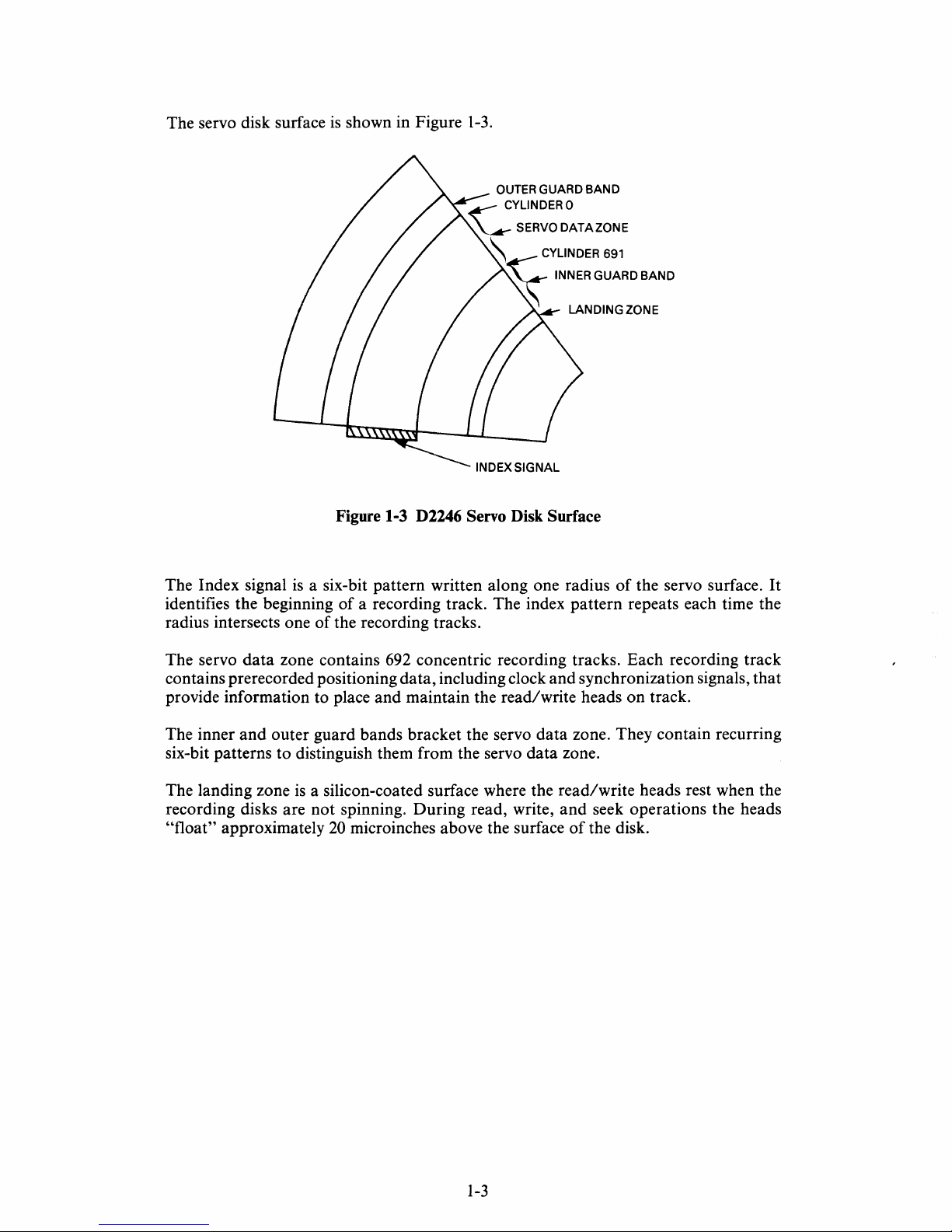
The servo disk surface
is
shown in Figure
1-3.
Figure 1-3 D2246 Servo Disk Surface
The Index signal
is
a six-bit pattern written along one radius
of
the servo surface.
It
identifies the beginning
of
a recording track. The index pattern repeats each time the
radius intersects one
of
the recording tracks.
The servo
data
zone contains 692 concentric recording tracks. Each recording track
contains prerecorded positioning data, including clock and synchronization signals, that
provide information to place and maintain the read/write heads on track.
The inner
and
outer guard bands bracket the servo data zone. They contain recurring
six-bit patterns to distinguish them from the servo data zone.
The landing zone
is
a silicon-coated surface where the read/write heads rest when the
recording disks are not spinning. During read, write,
and
seek operations the heads
"float"
approximately
20
microinches above the surface
of
the disk.
1-3
Page 14
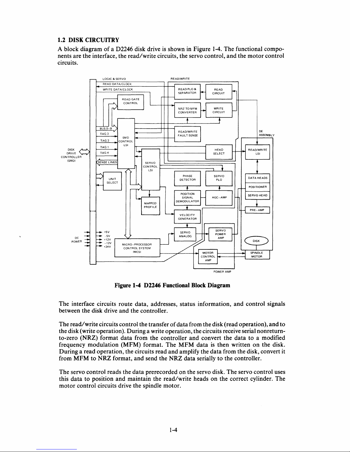
1.2 DISK
CIRCUITRY
A block diagram
of
a D2246 disk drive
is
shown
in
Figure 1-4. The functional components are the interface, the read/write circuits, the servo control, and the motor control
circuits.
~
DISK
DRIVE
CONTROLLE
(SMDI
DC
POWE
-
-
R:::::
-
r--
-
--
LOGIC & SERVO
READ/WRITE
READ
DATA/CLOCK
WRITE
DATA/CLOCK
J
READPLO&
READ
I
_
SEPARATOR
CIRCUIT
I
-a
"eA,GA"
CONTROL
I
NRZ
TO
MFM
WRITE
CONVERTER
CIRCUIT
f
j
~SO-9~
I
"eA","m
I
TAG
3
FAUL
T SENSE
SMD
I
TAG
2
CONTROL
TAG
1
LSI
!L.
I
HEAD
TAG
4
l
SELECT
-
A
SENSE
LINES
SERVO
~
CONTROL
,
l~
LSI
~
I
/I
PHASE
SERVO
UNIT
DETECTOR
PLO
t-
SELECT
It
r-
+
~
t
I
",m,o,
SIGNAL
AGC-AMP
MAPPED
DEMODULATOR
PROFILE
t
VELOCITY
j
GENERATOR
t
__
t5V
r H
SERVO
~
SERVO
POWER
__
-5V
ANALOG
AMP
f-+-
t12V
AMOTO"
I
r--
-12V
MICRO-PROCESSOR
r--
t24V
CONTROL
SYSTEM
(MCSI
/
-,
CONTROL
l
AMP
I
POWER AMP
Figure
1-4 D2246
Functional
Block
Diagram
r
~
DE
ASSEMBLY
"
r
-
H
"eA"WR'"
LSI
I
DATA
HEADS
r-
POSITIONER
I
SERVO
HEAD
lH
PRE-AMP
r
-
DISK
--,-
SPINDLE
I
MOTOR
L
The interface circuits route data, addresses, status information, and control signals
between the disk drive and the controller.
The read/write circuits control the transfer
of
data from the disk (read operation), and to
the disk (write operation). During a write operation, the circuits receive serial nonreturnto-zero
(NRZ) format data from the controller and convert the data to a modified
frequency modulation (MFM) format. The MFM data is then written
on
the disk.
During a read operation, the circuits read and amplify the data from the disk, convert it
from MFM to
NRZ format, and send the NRZ data serially to the controller.
The servo control reads the data prerecorded on the servo disk. The servo control uses
this data to position and maintain the read/write heads on the correct cylinder. The
motor control circuits drive the spindle motor.
1-4
Page 15
1.3 POWER REQUIREMENTS
D2246 disk drives operate on externally supplied dc power.
DC
power requirements are
listed in Table
1-1.
Table 1-1 DC Power Requirements
REQUIRED
DAMAGE
RIPPLE
VOLTAGE
TOLERANCE
THRESHOLD
CURRENT
(PEAK TO PEAK)
+5.0V
±0.25 V
±10%
4.0A
100mV
-5.0V
±0.25 V ±10%
0.5
A
100mV
+12.0V
±0.60 V ±10%
0.6
A
100mV
-12.0 V
±0.60 V
±10%
0.5
A
100
mV
+24.0 V
±2.40 V ±10%
2.5
A*
240mV
5.0 A**
*2.5 A - average running current
**5.0 A - peak starting current (25 seconds maximum duration)
All power line voltages must be established within
500 milliseconds (ms)
of
power on.
Voltages must be enabled in the following order: +5
V,
-5
V,
±12
V,
+24
V.
When power
is
turned off, lines must be disabled in the reverse order: +24
V,
±12
V,
-5
V,
+5
V.
1.4 FEATURES
Shorter access times, high-speed
data
transfers,
and
mechanical reliability are required
for efficient computer network operations. To meet these demands the D2246 disk drive
offers the following features.
1.4.1 Enhanced
Seek Time
Seek time
is
the time required to find requested
data
on the disk. The D2246 has
an
average seek time
of
25
milliseconds (ms), and a maximum
of
50
ms.
1.4.2 Rapid
Data
Transfer Rate
The D2246 provides a data transfer rate
of
approximately 1.2
MB
per second.
1.4.3 Compact Mounting
The compact size
of
the D2246 allows for either horizontal
or
vertical mounting in a
limited space. The drive's lock mechanism
is
easily accessible even after the drive has
been placed within a system cabinet.
The D2246 also features an integrated cooling fan
that
reduces space
and
power
requirements.
1-5
Page 16

1.4.4 Simplified Maintenance
The air-tight, sealed
disk/head
assembly
and
the D2246's simplified design produce a
disk drive
that
requires no periodic maintenance. Neither installation
nor
field service
requires special tools.
Motor
electronics are placed outside the
head/disk
assembly
and
do
not need "clean
room"
repair facilities.
An
optional diagnostic panel
is
available for test
and
maintenance purposes (see Appen-
dix C).
1.4.5 Design Reliability
Lightweight, contact-type
start/stop
heads
that
reduce damage
to
the heads
and
disks
are used within the D2246 disk drive. A simplified rotary actuator, a directly coupled,
brushless dc motor,
and
a closed-loop air circulation system are the drive's major
mechanical components. The control logic
is
microprocessor controlled
and
designed
to
minimize electronic components. This design strategy ensures high reliability
and
low
cost.
1.4.6 Standard Interfaces
The D2246 uses standard original equipment manufacturer interfaces for connection to a
disk controller and
to
a power supply.
1.4.7 Safety
The D2246 conforms to Underwriter's Laboratories Safety Regulation UL478.
1.4.8 System Configuration Flexibility
A maximum
of
four D2246 disk drives can be connected
to
a single controller in either a
daisy-chain
or
radial system (see Figures
1-5
and
1-6).
DISK DRIVE CONTROLLER
SG
AO
BO
B1
Bn
r
CABLEA
CABLE B
/
-
\
/
-
\
V
V
-
~
V
-
~
si)
A
IB~
A
IB-
A
Is~
*TERM
*TERM
*TERM
DISK DRIVE
DISK DRIVE
---
DISK DRIVE
0
1
4 (maximum)
* TERMINATING RESISTORS INSTALLED ON EACH DRIVE
Figure 1-5 Daisy-Chain System Configuration
1-6
Page 17
DISK DRIVE CONTROLLER
SG
AO
BO
SG
A1
B1
SG
An
Bn
S~
A
1;-
~~
A
1;-
S~
A
IB
....
*TERM
*TERM
*TERM
DISK DRIVE
DISK DRIVE
---
DISK DRIVE
a
1
4
(maximum)
* TERMINATING RESISTORS INSTALLED
ON
EACH DRIVE
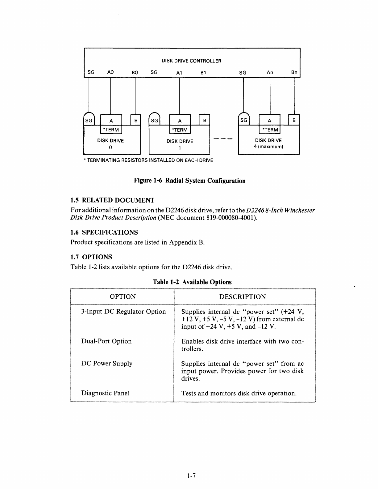
Figure 1-6 Radial System Configuration
1.5 RELATED
DOCUMENT
For
additional information on the D2246 disk drive, refer to the D2246 8-Inch Winchester
Disk
Drive Product Description (NEC document 819-000080-4001).
1.6 SPECIFICATIONS
Product
specifications are listed in Appendix
B.
1.7 OPTIONS
Table
1-2
lists available options for the D2246 disk drive.
Table 1-2 Available
Options
OPTION
DESCRIPTION
3-Input
DC
Regulator Option
Supplies internal dc
"power
set" (+24
V,
+
12
V,
+5
V,
-5
V,
-12
V)
from external dc
input
of
+24
V,
+5 V,
and
-12
V.
Dual-Port Option
!
Enables disk drive interface with two con-
I
trollers.
!
\.
DC
Power Supply
I
Supplies internal dc
"power
set"
from ac
input power. Provides power for two disk
drives.
Diagnostic Panel
I
Tests and monitors disk drive operation.
1-7
Page 18
Chapter
2
Installation
Procedures
This chapter provides procedures for installing a D2246 disk drive. When preparing the
installation site, refer to the environmental specifications listed in Appendix
B.
2.1
UNPACKINGIREPACKING
Before unpacking the disk drive, examine the shipping carton for damage.
If
damage has
occurred, notify the carrier immediately.
Do
not open the carton until the carrier's
representative
is
present.
If
there
is
no damage to the shipping carton, use these procedures to unpack the disk
drive. Failure to follow these procedures can void the product warranty.
1.
Open the top
of
the shipping carton.
2.
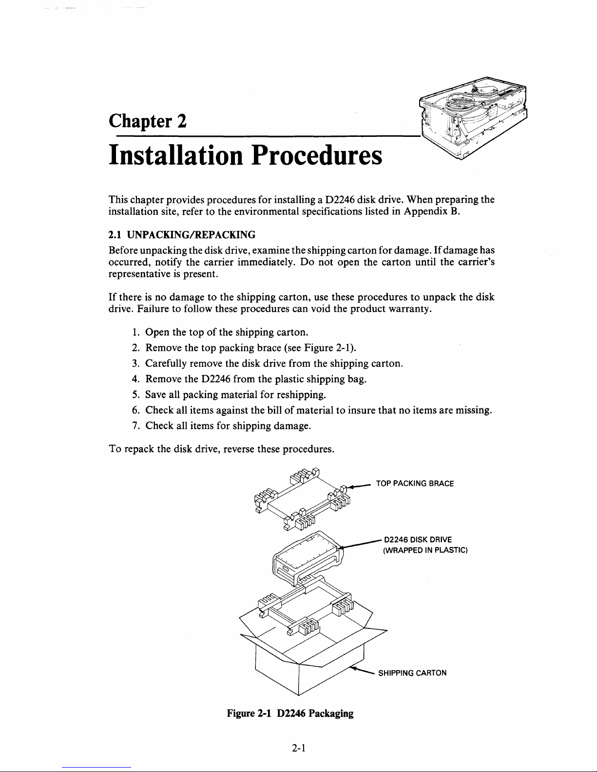
Remove the top packing brace (see Figure 2-1).
3.
Carefully remove the disk drive from the shipping carton.
4.
Remove the D2246 from the plastic shipping bag.
5.
Save all packing material for reshipping.
6.
Check all items against the bill
of
material to insure
that
no items are missing.
7.
Check all items for shipping damage.
To repack the disk drive, reverse these procedures.
TOP PACKING BRACE
02246
DISK DRIVE
SHIPPING
CARTON
Figure
2-1
D2246
Packaging
2-1
Page 19
2.2 TERMINATING RESISTORS
Terminating resistors are installed on the G9QST logic and servo printed circuit board
(PCB) as shown in Figure
2-2.
G9QST LOGIC
AND
SERVO
PCB
DCJC3
c:::::3.c]
CJD
~~
c:::::3
CJ
c:::J
c::J
CJ
0 0
c:::J
CJ~
[]
0 [JJ
0000
o 0
TERMINATING RESISTORS
Figure 2-2 G9QST Terminating Resistor and Jumper Locations
If
the D2246 drive
four terminating resistors in place as shown in Figure 2-3. Terminating resistors can be
either 150a
or
56
JUMPERS
EJ
~
lOB
is
connected to the controller in a radial configuration, install a set
JPl
CPU
RESET
JP6
FIRST
RETRY
I
JP8
FAULT (FAULT ENABLED)
lONE
STEP (JUMPER REMOVED)
ONIOFF
(RETRY
ENABLED)
n.
of
DISK DRIVE CONTROLLER
SG
~~
TERMINATING RESISTORS INSTALLED ON EACH DRIVE
*
AO
A
*TERM
DISK DRIVE
0
BO
r;-
SG
S~
A1
A
*TERM *TERM
DISK DRIVE
1
B1
r;-
Figure 2-3 Terminating Resistors
2-2
---
in
Radial System
SG
S~
An
A
DISK DRIVE
4 (maximum)
Bn
,;-
Page 20
In
a daisy-chain
configuration,
two
types
of
termination
methods
can
be
used.
To
terminate
individual drives, install a set
of
four
150n resistors in
each
drive as
shown
in
Figure 2-4.
DISK DRIVE CONTROLLER
SG
AO
BO
B1
Bn
r
CABLEA
CABLE B
- -
/
-
\ /
-
\
V
V
~
V
~
~~
A
IB~
A
I;
A
IB~
*TERM
*TERM *TERM
DISK DRIVE DISK DRIVE
---
DISK DRIVE
0
1
4
(maximum)
* TERMINATING RESISTORS INSTALLED ON EACH DRIVE
Figure 2-4 Individual Drive Termination/Daisy-Chain System
To
terminate
the last drive, install a set
of
four
56n
resistors in
the
final drive
of
the chain
as shown in Figure 2-5.
DISK DRIVE CONTROLLER
SG
AO
BO
B1
Bn
r
CABLEA
-
CABLE B
/
-
\ /
-
\
V
V
-
~
V
-
~
S~
I
A
I
ls-
I
A I
[B-
A
IB~
*TERM
DISK DRIVE
DISK DRIVE
---
DISK DRIVE
0
1
4
(maximum)
* TERMINATING RESISTORS INSTALLED ONLY ON LAST DRIVE
Figure 2-5
Last
Drive Termination/Daisy-Chain System
2-3
Page 21
2.3
JUMPER
Three
location
jumper
Figure 2-2. Insure
REQUIREMENTS
settings
of
these three
must
be verified before power is applied
jumpers
that
settings
Do not alter these
for factory adjustments only.
(JPl,
match
jumper
JP6,
and
those shown in Figure 2-2.
CAUTION
settings. They are intended
JP8)
on
the
to
the disk drive. The
G9QST
PCB
is
shown in
SWITCH
2.4
Three eight-segment, dual-inline-packaged
and
servo PCB configure
sector count.
SETTINGS
the
D2246 to communicate with the controller
DIP
switch assembly locations are shown in Figure 2-6.
INSTALLATION SWITCH
;\®i
CjJcsD
o
ornIIIIlJ
~C1
~CJ
SECTOR
SWITCH SWITCH
C1
DDO[]
C1
C]
DO
SELECT CONTROL MODE
C1C3
CJC3CJ
C]
C]
C]
C]
(DIP)
D
D
D
switch assemblies on the
0000000
o
C5
c:::::s
CJ
C3
C]
c:::J 0
C]
c::::::3
C]
~~CJ
DOD
~CJc=J
0000
o 0
G9QST
and
~
[]::J
logic
set the
Figure 2-6
DIP
Switch Assembly Locations
2-4
Page 22
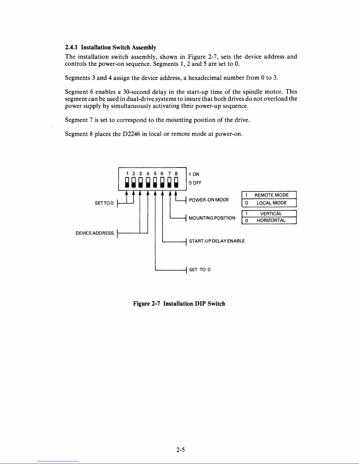
2.4.1 Installation Switch Assembly
The installation switch assembly, shown in Figure 2-7, sets the device address
and
controls the power-on sequence. Segments
1, 2 and
5 are set to
O.
Segments 3
and
4 assign the device address, a hexadecimal number from 0 to
3.
Segment 6 enables a 30-second delay in the start-up time
of
the spindle motor. This
segment can be used in dual-drive systems to insure
that
both
drives
do
not
overload the
power supply by simultaneously activating their power-up sequence.
Segment 7
is
set to correspond to the mounting position
of
the drive.
Segment 8 places the D2246 in local
or
remote mode
at
power-on.
SETTOO
DEVICEADDRESS
t----....L-...J
I'
ON
o
OFF
~---f
START -up DELAY ENABLE
~----f
SET
TO
0
Figure 2-7 Installation DIP Switch
2-5
1 REMOTE MODE
o LOCAL MODE
1 VERTICAL
o HORIZONTAL
Page 23

2.4.2 Control Mode Switch Assembly
The
control
mode
switch assembly (shown in Figure 2-8) configures the D2246
to
communicate
with the disk controller
and
enables certain
optional
drive features.
Segment 1
is
set
to
1.
Segments 2
and
3 are set
to
O.
Segment 4 enables the Address
Mark
function.
Segment 5 enables the
Read
Sector
function.
When
segments 5
and 7 of
the
control
mode
switch assembly
are
set
to
1,
Tag 4 can
be used with
bus
bits 8
and 9 to
request the
current
sector address.
The
D2246 issues the
current
sector address across the sense lines.
Segment 6 enables the
Format
Write Release
Option
used with some controllers.
Segment 7 enables the
Tag
4 line.
Segment 8 enables the controller interface.
SETTO
1
SET TO 0
1--_.1..-1
1 ON
OOFF
INTERFACE ENABLE
TAG 4 ENABLE
ON LINE
OFF LINE
L..-
__
.....
FORMAT
WRITE RELEASE ENABLE
ADDRESS
MARK
ENABLE
1-----
......
~----f
READ SECTOR ENABLE
Figure 2-8 Control Mode
DIP
Switch
2-6
Page 24

2.4.3 Sector Select Switch Assembly
The
sector select switch assembly (see Figure 2-9) sets the
number
of
sectors
per
track.
Any
number
of
sectors
up
to
128
can
be selected.
1 2 3 4 5 6 7 8 1
ON
~ ~
~
~
~
~ ~
~
0
OFF
SECTOR
COUNT
DISPOSITION SWITCH
Figure 2-9 Sector Select Switch
Segment 1
of
this assembly determines
the
disposition
of
odd
or
remainder
bytes. These
are
extra bytes
that
must
be allocated when the available bytes
per
track
are
not
evenly
divisible by the
number
of
sectors
per
track.
With
segment 1 in the 0 position,
odd
bytes
are
grouped
together
in
an
extra
sector
at
the
end
of
the
track.
With
this segment in the 1
position, the last sector
is
reduced
to
account
for
odd
bytes.
INDEX
Jl
n
If
PULSE
I
I
I
"SA"
"SA"
"SA"
"SA"
I
"SA"
I
SECTOR
0
n
1
~S
31
n
32
n(33)
I
0
rL
PULSE
F
"0"
(620
(620)
(620)
(620)
f-20~
(620)
BYTES
BYTE
I
(EXTRA
SECTOR)
I
"SA"
"SA"
"SA"
"SA"
I
"SA"
I
SECTOR
0
n
~$
31
n
32
I
0
rL
PULSE
(621)
(621 )
(621 )
608
BYTE
I
(621 )
F"1"
I
(LAST SECTOR)
Figure 2-10
Sector Allocation
Figure
2-10 illustrates the allocation
of
33
sectors with segment 1
of
the sector select
switch assembly in
both
the 0
and
1 positions.
2-7
Page 25
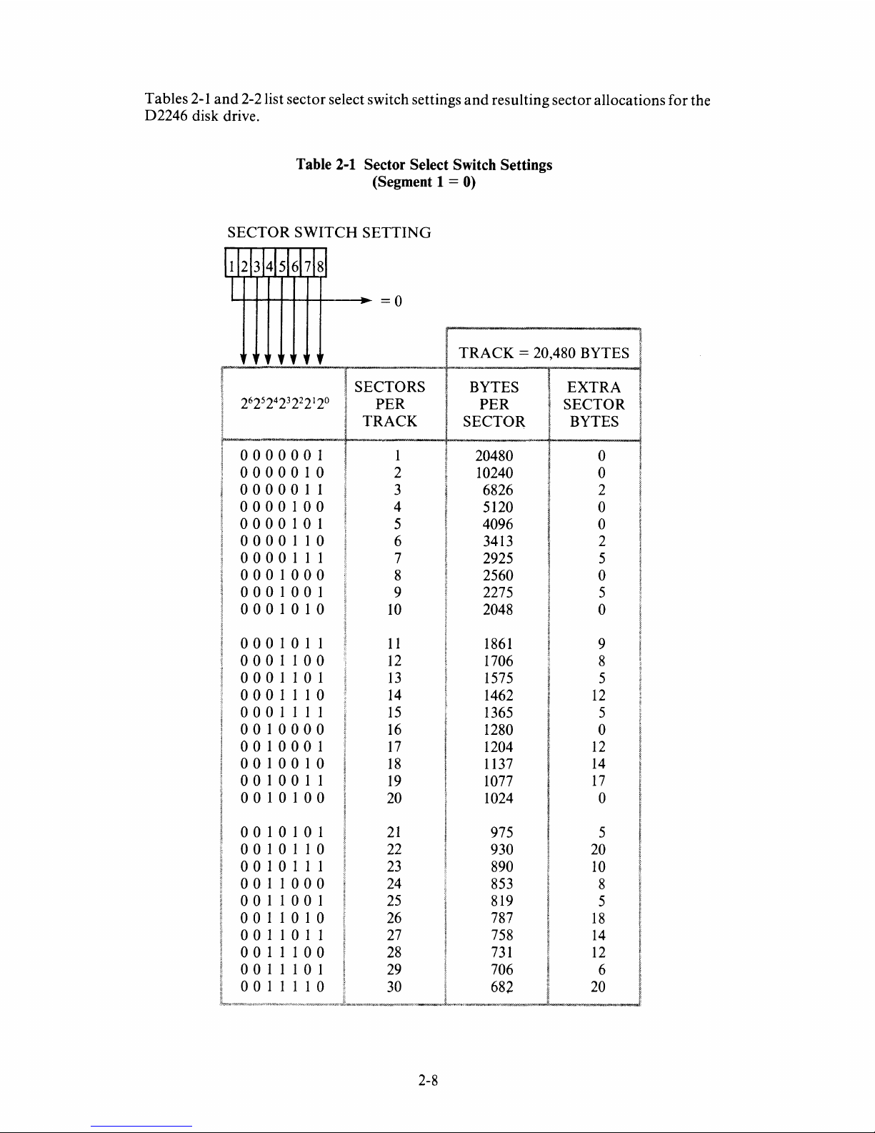
Tables
2-1
and
2-2
list sector select switch settings
and
resulting sector allocations for the
D2246
disk drive.
Table 2-1 Sector Select Switch Settings
(Segment 1
= 0)
SECTOR
SWITCH
SETTING
Id2bl41516bl81
,-+-I~~I-+-_.
= 0
, , , 1 1
If
TRACK
=
20,480
BYTES
SECTORS
2625242322212°
PER
TRACK
o 0 0 0 0 0 1 1
0000010
2
0000011
3
0000100
4
o 0 0 0
101
5
0000110
6
o 0 0 0 1 1 1 7
0001000
8
000
100
1 9
o 0 0 1 0 1 0
10
000
1 0 1 1
11
o 0 0 1 1 0 0
12
o 0 0 1 1 0 1
13
o 0 0 1 1 1 0
14
o 0 0 1 1 1 1
15
o 0 1 0 0 0 0
16
0010001
17
o 0 1 0 0 1 0
18
o 0 1 0 0 1 1
19
o 0 1 0 1 0 0
20
o 0 1 0 1 0 1
21
o 0 1 0 1 1 0
22
o 0 1 0 1 1 1
23
o 0 1 1
000
24
o 0 1 1 0 0 1
25
o 0 1 1 0 1 0
26
o 0 1 1 0 1 1
27
o 0 1 1 1 0 0
28
o 0 1 1 1 0 1
29
o 0 1 1 1 1 0
30
2-8
BYTES
PER
SECTOR
20480
10240
6826
5120
4096
3413
2925
2560
2275
2048
1861
1706
1575
1462
1365
1280
1204
1137
1077
1024
975
930
890
853
819
787
758
731
706
682
EXTRA
SECTOR
BYTES
o
o
2
o
o
2
5
o
5
o
9
8
5
12
5
o
12
14
17
o
5
20
10
8
5
18
14
12
6
20
Page 26
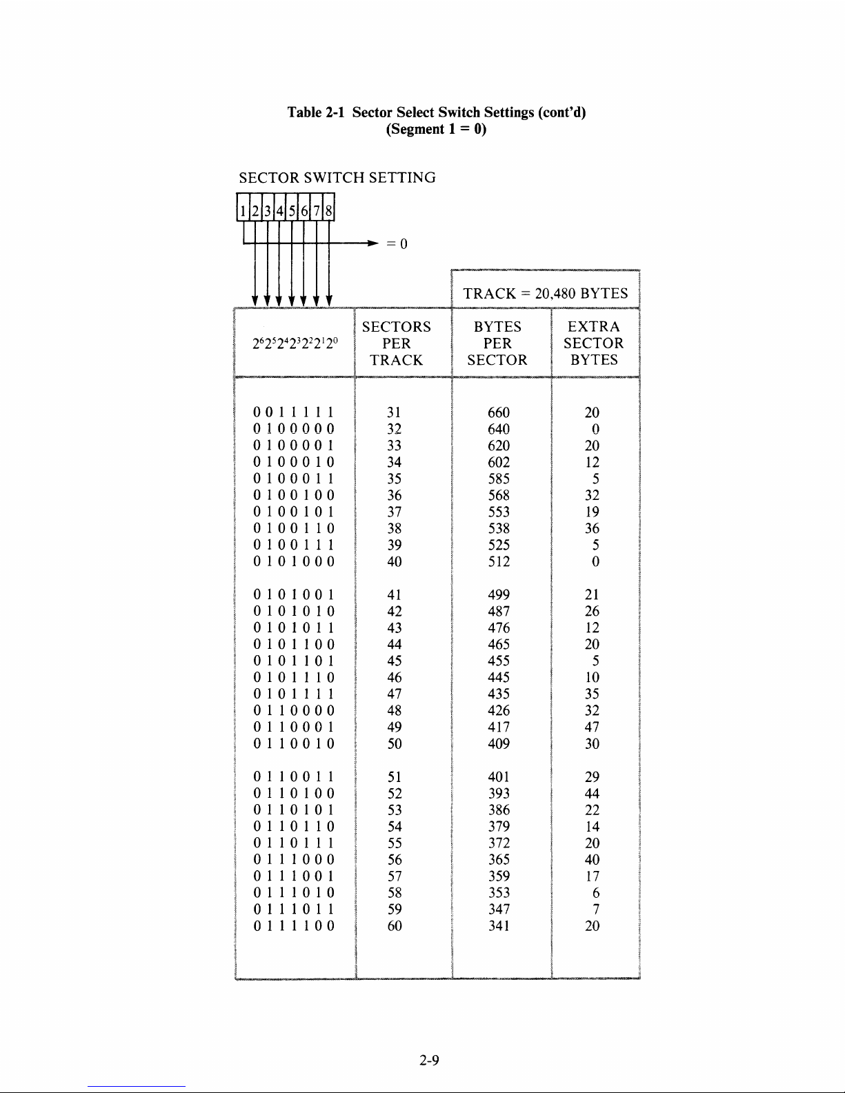
Table 2-1 Sector Select Switch Settings (cont'd)
(Segment 1
= 0)
SECTOR SWITCH
SETTING
112bI415/617/81
I-+I-+-+-+-+-+-+---
.....
~
= 0
I
!"
!
SECTORS
2625242322212°
PER
TRACK
0011111
31
o 1 0 0
000
32
o 1 0
000
1
33
o 1 0 0 0 1 0 34
o 1
000
1 1
35
o 1 0 0 1 0 0 36
o 1 0 0 1 0 1 37
o 1 0 0 1 1 0
38
o 1 0 0 1 1 1
39
o 1 0 1 0 0 0 40
o 1 0 1 0 0 1
41
o 1 0 1 0 1 0 42
o 1 0 1 0 1 1 43
0101100
44
o 1 0 1 1 0 1 45
o 1 0 1 1 1 0 46
o 1 0 1 1 1 1 47
o 1 1 0 0 0 0
48
o 1 1
000
1 49
o 1 1 0 0 1 0 50
o 1 1 0 0 1 1
51
o 1 1 0 1 0 0 52
o 1 1 0 1 0 1
53
o 1 1 0 1 1 0 54
o 1 1 0 1 1 1
55
o 1 1 1
000
56
o 1 1 1 0 0 1
57
o 1 1 1 0 1 0
58
o 1 1 1 0 1 1
59
o 1 1 1 1 0 0 60
2-9
TRACK
= 20,480 BYTES
BYTES
PER
SECTOR
660
640
620
602
585
568
553
538
525
512
499
487
476
465
455
445
435
426
417
409
401
393
386
379
372
365
359
353
347
341
EXTRA
SECTOR
BYTES
20
o
20
12
5
32
19
36
5
o
21
26
12
20
5
10
35
32
47
30
29
44
22
14
20
40
17
6
7
20
Page 27
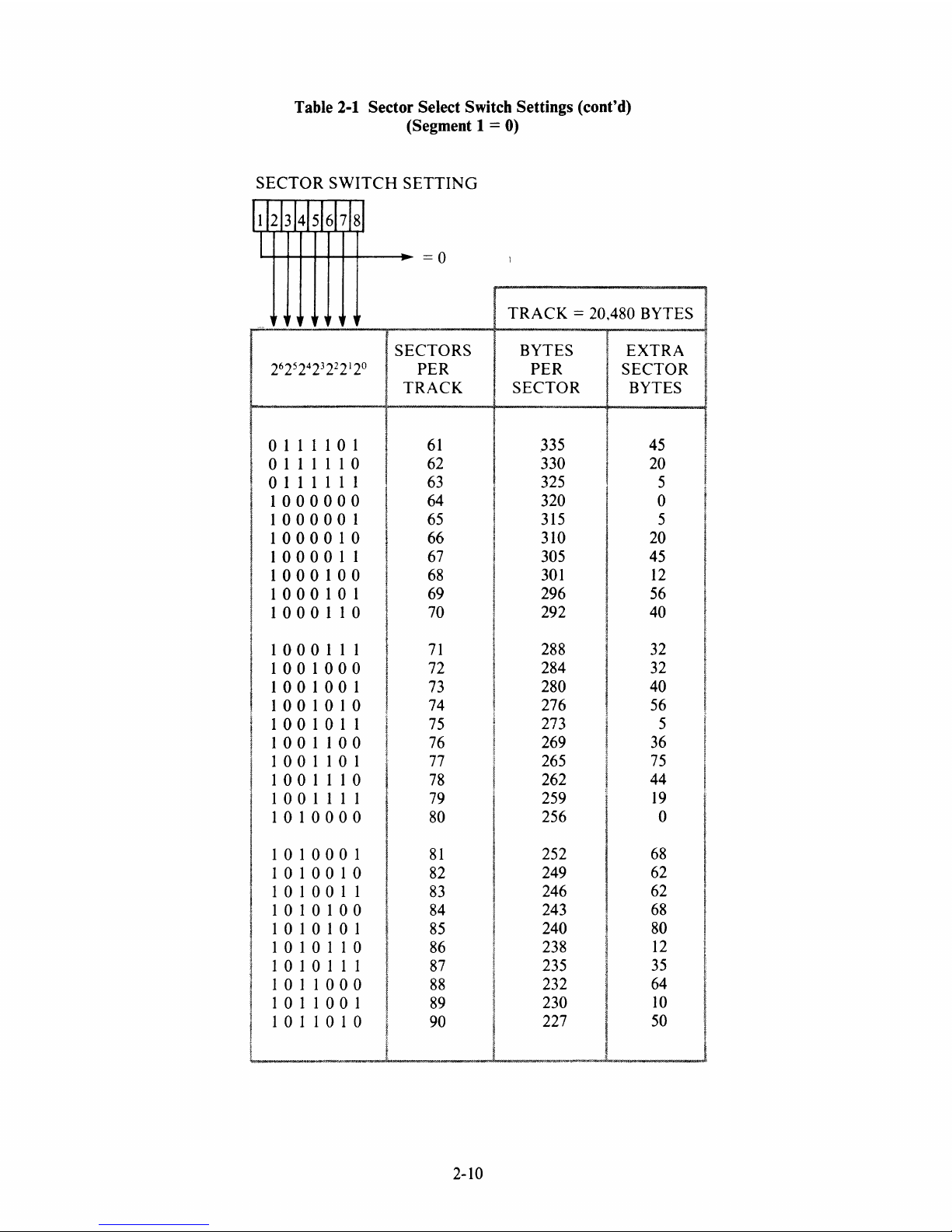
Table 2-1 Sector Select Switch Settings (cont'd)
(Segment 1
= 0)
SECTOR
SWITCH
SETTING
112b14[sf6b181
I~+-+-+--+-+----.
= 0
,
, , ,
SECTORS
2625242322212°
PER
o 1 1 1
101
0111110
0111111
1000000
1000001
1
000
0 1 0
1000011
1000100
1
000
101
1000110
1000111
1001000
100
100
1
1001010
1001011
!
1001100
I
1001101
'
1001110
1001111
1 0 1
000
0
1 0 1
000
1
1 0
100
1 0
1010011
1 0 1 0
100
1 0 1 0
101
1010110
1010111
1011000
1011001
1011010
TRACK
61
62
63
64
65
66
67
68
69
70
71
72
73
74
75
76
77
78
79
80
81
82
83
84
85
86
87
88
89
90
2-10
TRACK
= 20,480 BYTES
BYTES
PER
SECTOR
,335
330
325
320
315
310
305
301
296
292
288
284
280
276
273
269
265
262
259
256
252
249
246
243
240
238
235
232
230
227
EXTRA
SECTOR
BYTES
45
20
5
o
5
20
45
12
56
40
32
32
40
56
5
36
75
44
19
o
68
62
62
68
80
12
35
64
10
50
Page 28
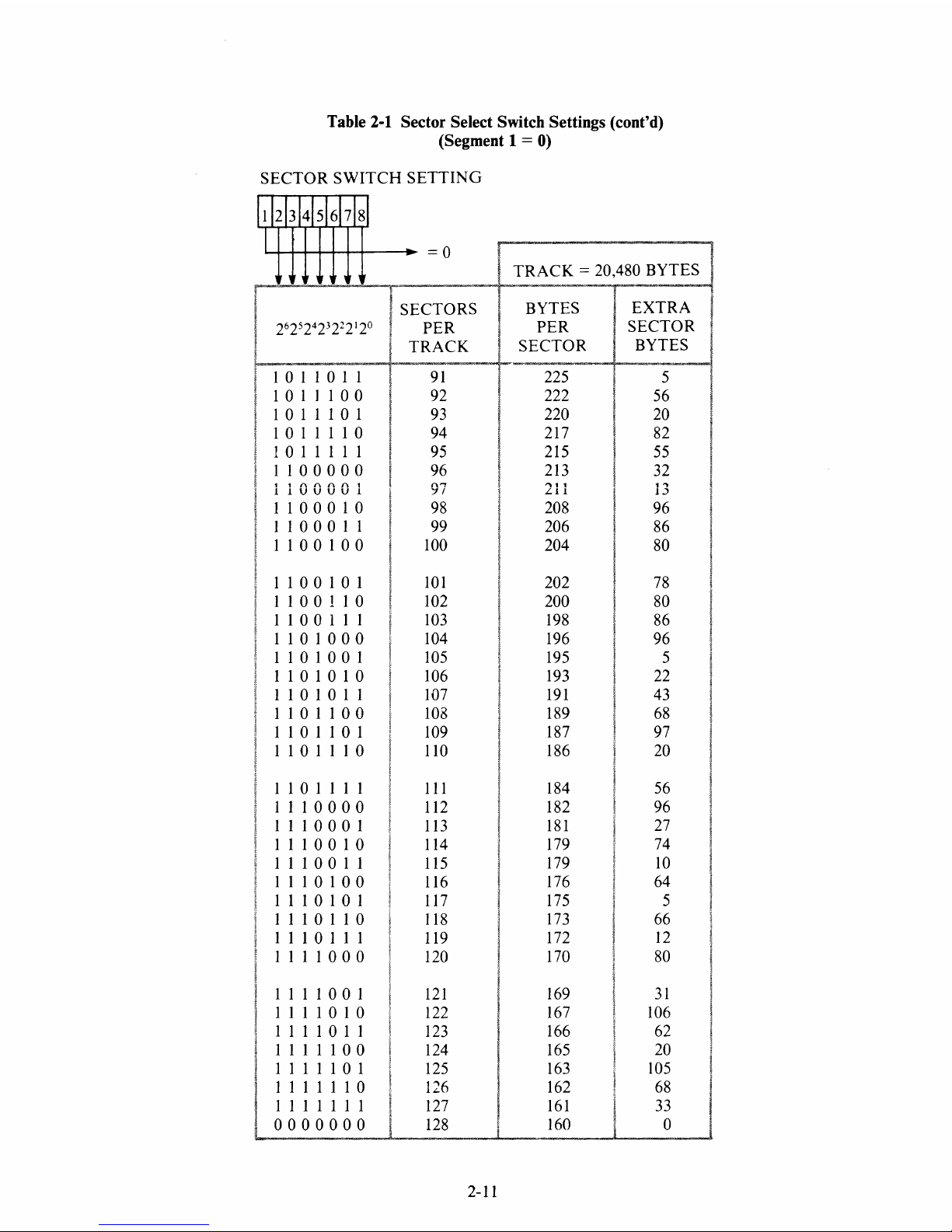
Table 2-1 Sector Select Switch Settings (cont'd)
(Segment 1
= 0)
SECTOR
SWITCH
SETTING
I d2bl41s1617181
L....+--41-+-+-+--+--+-----...
= 0
SECTORS
26252423222'2°
PER
TRACK
1 0 1 1 0 1 1
91
1 0 1 ] 1 0 0 92
1
0 1 1 1 0 1 93
1
0 1 1 1 1 0 94
1 0 1 1 1 1 1 95
1 1
0 0 0 0 0 96
1 1 0 0 0 0 1 97
1 1 0 0 0 1 0 98
1
1 0 0 0 1 1 99
1 1
0 0 1 0 0 100
1
100
101
1100110
1100111
1101000
110 1 001
1101010
1101011
1101100
1101101
1101110
1101111
1110000
1110001
1110010
1110011
1110100
1 1 1 0
101
1110110
1110111
1111000
1111001
1 1 1 1 0 1 0
1111011
1 1 1 1
100
1111101
1111110
1111111
0000000
101
102
103
104
105
106
107
108
109
110
111
112
113
114
115
116
117
118
119
120
121
122
123
124
125
126
127
128
2-11
TRACK
= 20,480
BYTES
BYTES
PER
SECTOR
225
222
220
217
215
213
"'11
L.l
1
208
206
204
202
200
198
196
195
193
191
189
187
186
184
182
181
179
179
176
175
173
172
170
169
167
166
165
163
162
161
160
EXTRA
SECTOR
BYTES
5
56
20
82
55
32
13
96
86
80
78
80
86
96
5
22
43
68
97
20
56
96
27
74
10
64
5
66
12
80
31
106
62
20
105
68
33
o
Page 29
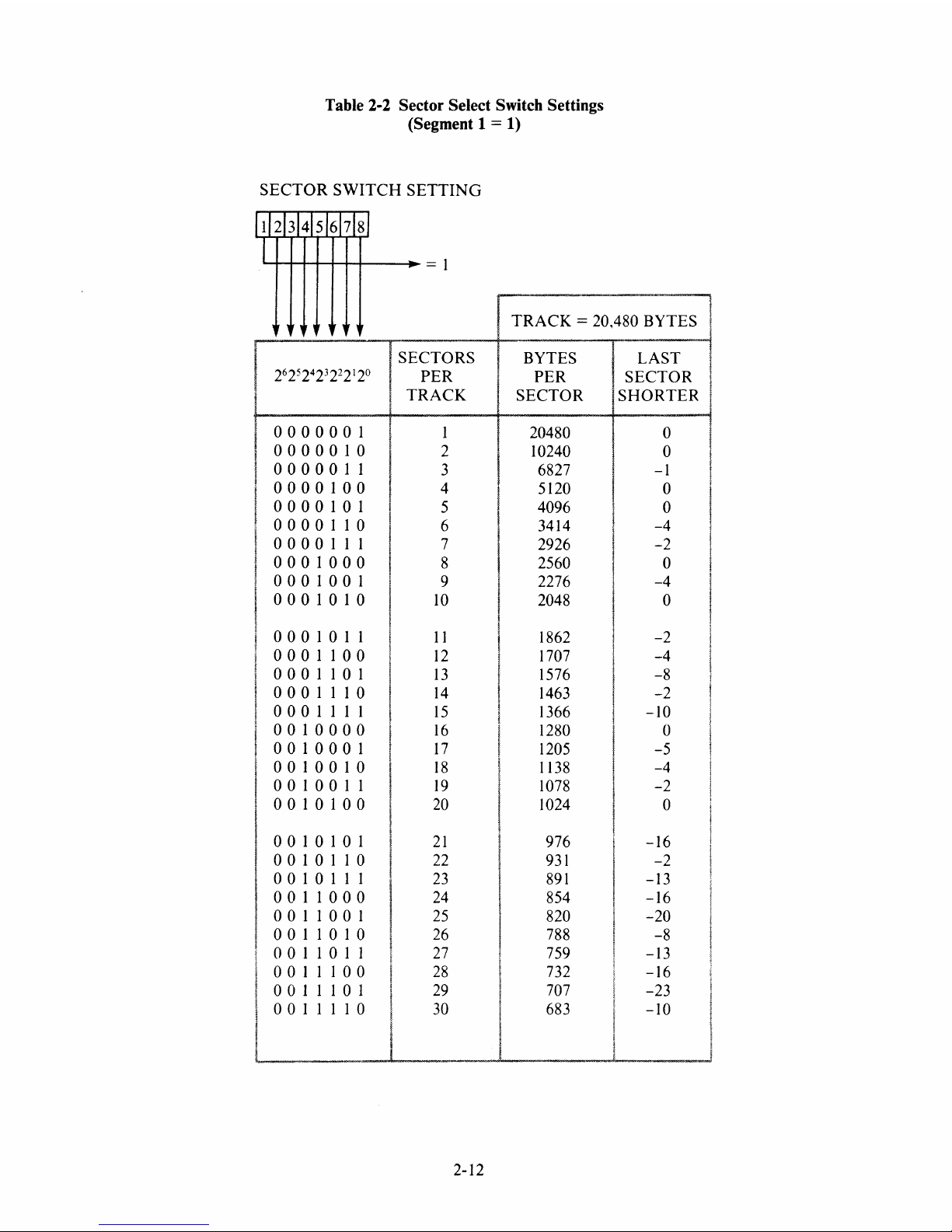
Table 2-2 Sector Select Switch Settings
(Segment 1
= 1)
SECTOR SWITCH SETTING
112/314151617181
'L+-H-+--+--4--+--
.... = 1
, , , •
1~
I TRACK =
20,480
BYTES
SECTORS
2625242322212°
PER
TRACK
o 0 0 0 0 0 1 1
0000010
2
0000011
3
0000100
4
o 0 0 0
101
5
0000110
6
0000111
7
0001000
8
0001001
9
o 0 0 1 0 1 0
10
0001011
0001100
0001101
0001110
0001111
0010000
o 0
100
0 1
o 0
100
1 0
0010011
o 0 1 0
100
o 0 1 0
101
0010110
0010111
0011000
0011001
0011010
0011011
0011100
0011101
0011110
11
12
13
14
15
16
17
18
19
20
21
22
23
24
25
26
27
28
29
30
2-12
BYTES
PER
SECTOR
20480
10240
6827
5120
4096
3414
2926
2560
2276
2048
1862
1707
1576
1463
1366
1280
1205
1138
1078
1024
976
931
891
854
820
788
759
732
707
683
LAST
SECTOR
SHORTER
o
o
-1
o
o
-4
-2
o
-4
o
-2
-4
-8
-2
-10
o
-5
-4
-2
o
-16
-2
-13
-16
-20
-8
-13
-16
-23
-10
Page 30
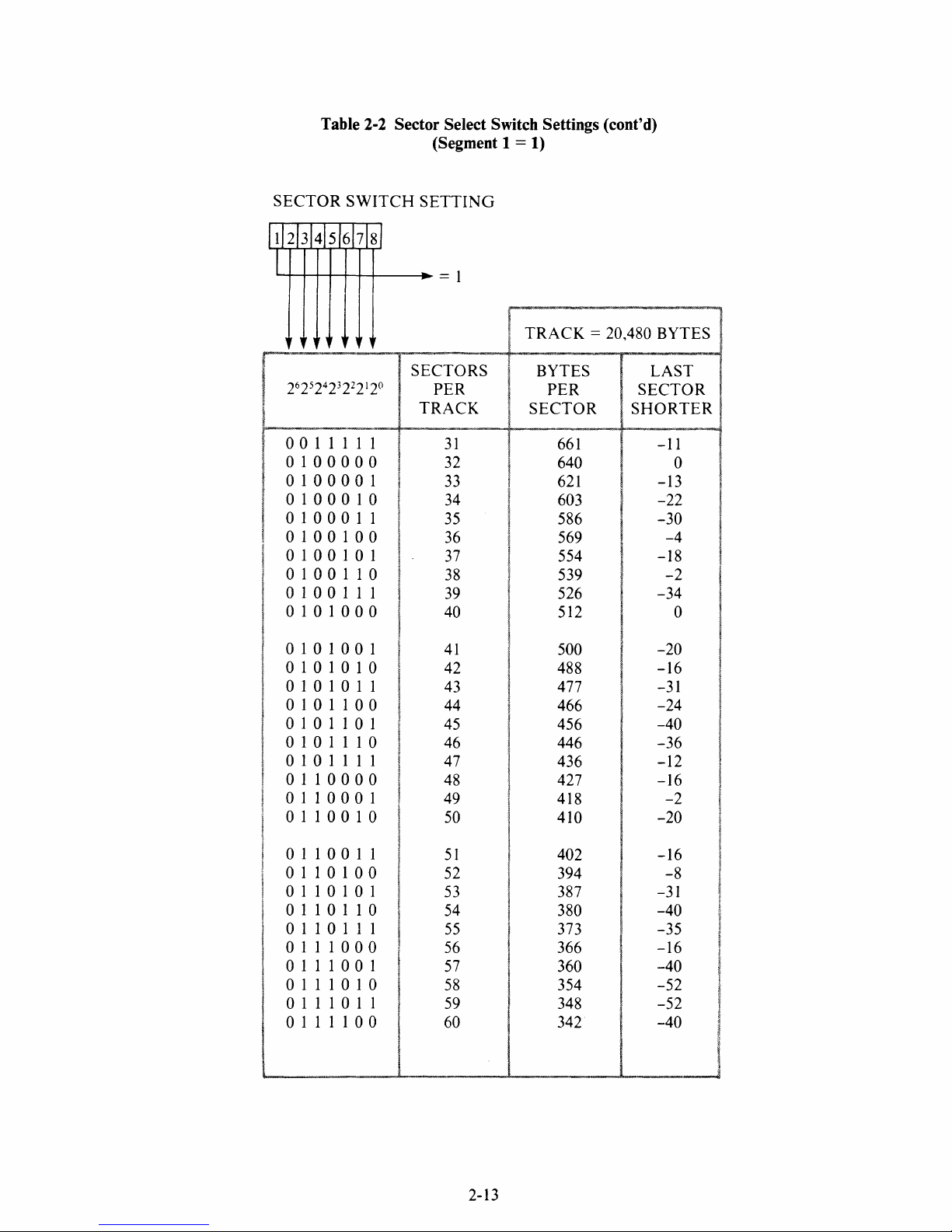
Table 2-2 Sector Select Switch Settings (cont'd)
(Segment 1
= 1)
SECTOR
SWITCH
SETTING
/1/213141516/718/
I~+-+-+-+-+-~
= 1
,
SECTORS
26252423222'2°
PER
TRACK
0011111
31
o 1 0
000
0 32
o 1 0 0 0 0 1
33
o 1
000
1 0 34
o 1 0 0 0 1 1
35
o 1 0 0 1 0 0
36
o 1 0 0 1 0 1
37
o 1 0 0 1 1 0
38
o 1 0 0 1 1 1
39
o 1 0 1
000
40
010
100
1
0101010
0101011
0101100
0101101
I"
0101110
j
010 1 111
I
0110000
II',
0110001
0110010
0110011
0110100
0110101
I
0110110
I,
0110111
0111000
0111001
0111010
0111011
0111100
41
42
43
44
45
46
47
48
49
50
51
52
53
54
55
56
57
58
59
60
2-13
TRJ-\CK = 20,480 BYTES
BYTES
PER
SECTOR
661
640
621
603
586
569
554
539
526
512
500
488
477
466
456
446
436
427
418
410
402
394
387
380
373
366
360
354
348
342
LAST
SECTOR
SHORTER
-11
o
-13
-22
-30
-4
-18
-2
-34
o
-20
-16
-31
-24
-40
-36
-12
-16
-2
-20
-16
-8
-31
-40
-35
-16
-40
-52
-52
-40
I
I
I
I
i
I
I
I
,
t
i
~
i
Page 31

Table 2-2 Sector Select Switch Settings (cont'd)
(Segment 1
= 1)
SECTOR SWITCH
SETTING
1/2/3/4/5/6/7181
l............-+-t-t---1r--t-+--
... = 1
, , , ,
SECTORS
2625242322212°
PER
0111101
0111110
0111111
1000000
100
000
1
1
0 0 0 0 1 0
1000011
1
000
100
1
000
101
1000110
1000111
100
100
0
100 1 001
100
1 0 1 0
1001011
1001100
1001101
1001110
100
1 1 1 1
1
0 1
000
0
1 0 1
000
1
1
0
100
1 0
1010011
1 0 1 0
100
1 0 1 0
101
1010110
1 0
101
1 1
1011000
1011001
1011010
TRACK
61
62
63
64
65
66
67
68
69
70
71
72
73
74
75
76
77
78
79
80
81
82
83
84
85
86
87
88
89
90
2-14
i
TR/\CK
= 20,480
BY
!
t:~
BYTES
PER
SECTOR
336
331
326
320
316
311
306
302
297
293
289
285
281
277
274
270
266
263
260
256
253
250
247
244
241
239
236
233
231
228
LAST
SECTOR
SHORTER
-16
-42
-58
o
-60
-46
-22
-56
-13
-30
-39
-40
-33
-18
-70
-40
-2
-34
-60
o
-13
-20
-21
-16
-5
-74
-52
-24
-79
-40
Page 32

I
Table 2-2 Sector Select Switch Settings (cont'd)
(Segment 1
= 1)
SECTOR SWITCH SETTING
~
= 1
TRACK
=
20,480
BYTES
11121314151617181
'HHH!
SECTORS
BYTES
LAST
2625242322212°
PER
PER
SECTOR
TRACK
SECTOR
SHORTER
1011011
91
226
-86
1011100
92
223
-36
1011101
93
221
-73
1011110
94
218
-12
1011111
95
216
-40
1100000
96
214
-64
1100001
97
212
-84
1100010
98
209
-2
1100011
99
207
-13
1100100
100
205
-20
1100101
101
203
-23
1100110
102
201
-22
1
100
1 1 1
103
199
-17
1101000
104
197
-8
1101001
105
196
-100
1101010
106
194
-84
1101011
107
192
-64
1101100
108
190
-40
1101101
109 188
-12
1101110
110
187
-90
1101111
111
185
-55
1110000
112
183
-16
1110001
113
182
-86
1 1
100
1 0
114 180
-40
1 1
100
1 1
115
179
-105
1 1 1
0
100
116 177
-52
1
110
101
117
176
-112
1110110
118
174
-52
1110111
119
173
-107
111 1 000
120
!
171
-40
1 1 1
100
1
121
170
-90
1 1 1 1 0 1 0
122
168
-16
1111011
123
167
-61
111 1 100
124
166
-104
1111101
125
164
-20
1111110
126
163
-58
1111111
127
162
-94
0000000
128
160
0
2-15
Page 33

2.5
CABINETIRACK
INSTALLATION
The mounting bracket (see Figure 2-11) shipped with the D2246 secures the disk drive
when it
is
installed in a cabinet
or
rack.
Figure
2-11
Mounting
Bracket
The drive can be installed in either a horizontal
or
vertical position as shown in Figure
2-12. Figure 2-12 also shows the required ventilation for each mounting position. An air
flow
of
1.1
cubic yards per minute
(1.1
yd3/min)
is
required on a O.4-inch surface.
NOTE
Be
certain
that
the segment 7
of
the installation
switch assembly
is
set according to the mounting
position (see Section 2.4.1).
HORIZONTAL INSTALLATION
Figure
2-12
Horizontal
and
Vertical
Installation
When installing the disk drive, first verify that the mounting holes in the rack
or
cabinet
align with the holes in the mounting bracket. Refer to Appendix B for information on
unit dimensions.
2-16
Page 34

2.6 CABLE
CONNECTIONS
This section describes the different connectors for the interface signal cables (cables A
and
B),
for
the system
ground
cable,
and
for the
power
cable.
2.6.1 Interface Cables
Interface cables
A
and
B are connected
to
the
G9QST
PCB
as
shown
in Figure 2-13.
~
PIN 1 MARK
02246
~
POWER
CABLE------.
B CABLE
-
I
-k~_®u
G9QST
PCB
P1:
] A CABLE
{
:1
r---
j
.
:~----~
L---.l:~===:E=t:~~~
Figure 2-13
Interface
Cable Connections
Cable B should
not
exceed 49.2
ft
(15 m) in length. Cable A should
not
exceed 98.4 ft (30 m)
in length.
In
a daisy-chain system, the
total
length
of
cable A
(from
the controller
to
the
last drive) should
not
exceed 98.4
ft
(see Figure· 2-14).
DISK DRIVE CONTROLLER
SG
AO
BO
B1
Bn
r
CABLEA
CABLE B
-
-
/ \ /
\
/
I
-
~
V
-
~
~~
A
fa-
A
r
B
-
A
rs-
*TERM
*TERM
*TERM
DISK DRIVE DISK DRIVE
---
DISK DRIVE
0
1
4 (maximum)
'-
98.4'
MAXIMUM
j
* TERMINATING RESISTORS INSTALLED
ON
EACH DRIVE
Figure 2-14 Cable AlDaisy-Chain System
2-17
Page 35

2.6.2 System Ground Cable
Connect
a system
ground
cable
to
the signal
ground
(SG) terminal
at
the
rear
of
the disk
drive (see Figure 2-15).
SG (SIGNAL GROUND) TERMINAL
POWER CONNECTOR
(P3)
Figure 2-15 Signal Ground and Power Connections
2.6.3 Power Cable
Connect
the
power
cable
to
connector
P3
at
the rear
of
the disk drive (see Figure 2-15).
2.7
LOCK
CONTROL
ASSEMBLY
When
the disk drive
is
shipped, the spindle
and
actuator
positioner are secured with a
lock device
to
prevent movement. This lock must be released
prior
to
operating the drive.
To
unlock the spindle
and
actuator,
slide the lock
control
lever
to
the
FREE
position (see
Figure 2-16).
I
IliD
LOCK LEVER
Figure 2-16 Lock Control Assembly
2-18
Page 36

Chapter
3
Preventive
Maintenance
and
Troubleshooting
This
chapter
outlines maintenance
and
troubleshooting
procedures
for
the D2246 disk
drive.
It
describes preventive
maintenance,
test
operations
and
test points,
and
asso-
ciated waveforms. Refer
to
Appendix C for
information
on
how
to
use the
optional
diagnostic panel.
3.1 GENERAL MAINTENANCE
RULES
Always observe the following general rules when replacing
parts
or
servicing the disk
drive.
•
Turn
off
the disk drive
and
disconnect all ac
power
to
the
drive
power
supply
before performing
any
maintenance procedure
on
the drive.
• Never remove
or
install
any
PCB,
or
disconnect
any
connector,
plug,
or
wire
while
power
is
on.
•
When
removing
any
connector,
grasp
it firmly
by
its sides
and
pull it
out.
Do
not
remove any connector by pulling
on
the wire bundle.
•
Do
not
remove
any
parts
that
are
not
specified in the replacement procedures.
• Package PCBs in
an
electrostatic-free envelope when they
are
transported.
3.2 MAINTENANCE
TOOLS
Standard
maintenance procedures require the following
common
hand
tools.
•
No.1
Phillips screwdriver
•
No.2
Phillips screwdriver
• Small straight-tip screwdriver
The following instruments are also required.
• High impedance voltmeter
• Oscilloscope (Tektronics 465
or
equivalent)
A
rotor
handler
(NEC
part
number
134-233280)
and
a diagnostic panel
(NEC
part
number
134-200267) are recommended.
3-1
Page 37

3.3 PREVENTIVE MAINTENANCE
Preventive maintenance
is
limited to periodic dusting
of
the surface
of
the drive. No
lubrication
or
further cleaning
is
required
or
recommended. D2246 disk drives contain
no parts
that
require scheduled adjustment
or
replacement.
NOTE
The air filter in the sealed
head/disk
assembly can-
not be replaced
or
cleaned.
As
part
of
a periodic preventive maintenance routine,
run
system-specific (software)
diagnostic programs
or
use the diagnostic panel to
run
offline test procedures (see
Appendix C).
3.4
TROUBLESHOOTING
If
a fault occurs, attempt
to
isolate the fault
to
the host, to the host controller,
to
the disk
drive,
or
to another connecting component.
For
faults isolated to the disk drive, use the
troubleshooting procedures outlined in the following flowcharts. These procedures
localize the fault to a specific drive component.
Figure 3-1 Troubleshooting Flowcharts
3-2
Page 38

W
I
W
-
~
READJUST
INSTALLATION
CH
ECK/REPLACF
DC
POWER
SUPPLY
UNIT
CHECK FOR
SHORT
IN CABLE
OR DRIVE
CONTINUE
T&D
REPLACE
DRIVE
CONTINUE
1 & D
HEPLACE
LOGIC
& SERVO
PCB
CONTINUE
T&D
REPLACE
FAILED
COMPONENTS
REPLACE
DRIVE
CHECK/REPLACE
CONTROLLER
PCB
CONTINUE
T&D
Figure 3-1 Troubleshooting Flowcharts (cont'd)
CONTINUE
T&D
CONTINUE
T & D
Page 39

W
I
VI
0\
9
CHECK
MOTOR
START
REPLACE
LOGIC
& SERVO
PCB
REPLACE
DRIVE
CHECK
LOCK
ASSEMBLY
REPLACE
POWER
AMP
PCB
REPLACE
DRIVE
CONTINUE
T&D
CONTINUE
T&D
REPLACE
DRIVE
CONTINUE
T&D
CONTINUE
T&D
CONTINUE
T&D
<
CONTINUE
T&D
REPLACE
POWER
AMP
PCB
REPLACE
LOGIC
& SERVO
PCB
[
REPLACE
DRIVE
-
Figure 3-1 Troubleshooting Flowcharts (cont'd)
CONTINUE
T&D
CONTINUE
T&D
Page 40

N
REPLACE
LOGIC
& SERVO
PCB
REPLACE
DRIVE
RUN DIAG-
NOSTICS
REPLACE
DRIVE
CONTINUE
T&D
REPLACE
FAILED
COMPONENTS
REPLACE
DRIVE
Figure
3-1
Troubleshooting
Flowcharts
(cont'd)
3-7
CONTINUE
T
r.
D
Page 41

N
REPLACE
LOGIC
& SERVO
PCB
CHECK
SE~UENCE
HOLD
REPLACE
DRIVE
RUN
DIAG-
NOSTICS
REPLACE
DRIVE
CONTINUE
T&D
CONTINUE
T & D
REPLACE
FAILED
COMPONENTS
N
REPLACE
DRIVE
Figure
3-1
Troubleshooting
Flowcharts
(cont'd)
3-8
CONTINUE
T&D
Page 42

REPLACE
FAILED
COMPONENTS
REPLACE
LOGIC
PCB
CHECK
SOFTWARE
& SERVO
REPLACE
DRIVE
CONTINUE
1&D
REPLACE
DRIVE
CONTINUE
T&D
REPLACE
DRIVE
Figure
CONTINUE
T&D
3-1
Troubleshooting Flowcharts (cont'd)
3-9
Page 43

9
CHECK
STATUS
TAG 1
CHECK CYLINDER
ADDRESS(ES)
CAUSING
ERROR
REPLACE
DRIVE
CHECK/REPLACE
INTERFACE
CABLES
N
REPLACE
& SERVO
LOGIC
PCB
CONTINUE
T&D
CONTINUE
T & 0
CONTINUE
T&D
Figure
3-1
Troubleshooting
REPLACE
CONTROLLER
PCB
REPLACE
DRIVE
3-10
Flowcharts
CONTINUE
T&D
(cont'd)
Page 44

Figure 3-1 Troubleshooting Flowcharts (cont'd)
3-11
Page 45

CHECK
HEAD
ADDRESSIESI
CAUSING ERROR
CHECK
SERVO
CLOCK
REPLACE
LOGIC
& SERVO
PCB
REPLACE
DRIVE
CONTINUE
T&D
REPLACE
CONTROLLER
PCB
REPLACE
DRIVE
REPLACE
LOGIC
& SERVO
PCB
REPLACE
READ/WRITE
PCB
REPLACE
DRIVE
CONTINUE
T&D
Figure
3-1
Troubleshooting
Flowcharts
(cont'd)
3-12
CONTINUE
T&D
CONTINUE
T&D
Page 46

3.5 SERVO SYSTEM SIGNALS
on
Test point locations
3-1
lists the signal
the G9QST logic
output
and
TP1
signal level from each test point.
!M
C5
C]
c=J~
[:=J
C5
and
servo PCB are shown in Figure 3-2. Table
TP9
THROUGH
~
TP15
~C5
~c:=3
~Q
c::::J
c::::=3
CJ
C5 C5
DDDu
C5
DOD
c::::J
[:=J
c::::=3
D~c=o
I
c::::J
D D
~DDU~
Figure 3-2 G9QST Test Point Locations
jDD
o\<
TP2
c::J
0
TP7
TP3
TP4
TP5
3-13
Page 47

Table 3-1 Test Point Signal Outputs
TEST
POINT
SIGNAL
LEVEL
TP2-2
Tripulse input (positive polarity) 20-75 mVpp
TP2-3
Tripulse input (negative polarity) 20-75 mVpp
TP3
Automatic gain control (AGC)
1.1
V (approx)
standard voltage
(regulated by
RV1)
TP4
AGC
control voltage
6.0 V (appro
x)
TP5
Tripulse
output
(AGC
output)
4.0 Vpp (appro x)
TP6
Q position signal
o to
±5.6
V
TP7
N position signal o to
±5.6
V
TP8
Not
used
I
TP9
Connected to
GND
during
2.0 V (approx)
offset adjustment
I
(see Section 5.2)
I
TP10 S peed set signal
I
o to +6.0 V
!
TPll
Speed signal (reverse
!
o to
-6.0
V
!
!
polarity to TP10)
I
TP12 Noise injunction terminal
I
o to 2.0 Vpp
I
TP13
I
Position loop phase
compensation filter input
TP14
Position loop secondary
I
filter
output
TP15 Servo current
o to 3.0 Vpp
(1.0 V corresponds to 1.0A)
Normal
servo system signals match the specifications
and
waveforms listed in Table 3-2.
3-14
Page 48

Table 3-2 G9QST Servo Signals
FUNCTIO~';
TEST
ponN·~'T'J.1
Tripulse input TP2-2, TP2-3
amplitude
AGC
output
TP5
amplitude
!
40mVpp~pp~150mVpp
and
Cylinder
COMMENTS
691
at
Cylinder 000
AGC
standard
voltage
TP3
VO, VE =
DC
about
About
1.0V
1.0 VO-p
3-15
Page 49

Table 3-2 G9QST Servo Signals (cont'd)
FUNCTION
Position signal
amplitude
I
!
I
I
I
I
I
Seek time
I
TEST
TP6, TP7
TPI-4
G9QST
the trigger.
POI~
of
is
1
000
~
TP7
COMMENTS
691
Cylinder Repeat Seek
E
I TP6 - If
I
E
i
000
~
:~====~~3~.8V
6gr
Cylinder Repeat Seek
+5.6
-------.
_~
----HH+---+----
'-
--3.8V
3.8V
-5.6
+5.6
3.8V
----
1/
-5.6
t
I
!
!
I
TP7
TPI-5
3-16
~
I-
*The settling time
41-43
is
ms
not
L
------l
included.
Page 50

Table 3-2 G9QST Servo Signals (cont'd)
FUNCTIOi-I\...~'
j'
TEST
POINT
Current waveform TP15
S peed profile
follows
Position
transient
response
The trigger
is
TPI-4
and
TPI-3
of
G9QST.
TPIO,
TPll
The trigger
is
TPI-4
and
TPI-3
of
G9QST.
TP7
The trigger
is
TPI-5
of
G9QST.
3-17
COMMENTS
000
~
691
Cylinder Repeat Seek
VI + 1.0 -
1.3
V
V2
< 1.3 V
(The polarity changes according to
the seek direction.)
000
~
691
Cylinder Repeat Seek
The speed set signal
(TPIO)
is
inverted
and
made to overlap
the speed signal
(TPII).
av
Optional seek
Va
va
~,
6,
t / f
c::>
If
there
is
an overshoot
VO<I VO-p
I
';/7-c-~
V 3 ms The amplitude 3ms
I after the position
mode
is
set shall
be less then
0.5VOP·
Page 51

3.6 SEEK OPERATIONS TESTING
A repeat seek
or
a one-cylinder seek operation can be initiated by connecting strapping
wire
to
TPI.
3.6.1 Repeat Seek Operation
A repeat seek
operation
seeks from the low cylinder (cylinder 000)
to
the high cylinder
(cylinder 691),
and
then from the high cylinder back
to
the low cylinder.
To
perform a
repeat seek operation, connect wires to
TPI
as shown in Figure 3-3.
5 0
10
?
TP1
TESTPOINT
o
o
o
o
IF
PINS 6
AND
7 ARE CONNECTED, THE SEEK
INTERVAL TIME
IS
100
MILLISECONDS.
Figure 3-3 Repeat Seek Using
TPI
3.6.2 One-Cylinder Seek Operation
A one-cylinder seek operation seeks from cylinder
000,
to
cylinder 001,
to
cylinder 002,
and
continues
to
the high cylinder.
From
the high cylinder, the unit seeks
to
cylinder 690,
to
cylinder 689,
and
continues back to the low cylinder.
To
perform a one-cylinder seek
operation, connect wires
to
TPI
as shown in Figure 3-4.
5 0
10
0
TP1
TESTPOINT
o
?
o
o
IF
PINS 6 AND 7 ARE CONNECTED, THE SEEK
INTERVAL TIME
IS
1.5 SECONDS.
Figure 3-4 One-Cylinder Seek Using
TPI
3-18
Page 52

Chapter
4
Removal
and
Procedures
This
chapter
assemblies. Field-replaceable items are listed in Table 4-1.
4.1 G9QST
Follow these steps
provides procedures for removing
Table 4-1 D2246 Field Replaceable Components
CO~v1PONENT/
G9QST Logic
G9QSQ
G9QSN
Earth
Motor
(LOGIC
Power Amplifier PCB 134-832951
Read/Write
Pad
Stator
AND SERVO) PCB REMOVAL
to
remove the G9QST logic
ASSEMBLY
and
Servo PCB 134-832954
PCB 134-832949
Assembly 134-232861-0
Assembly 806-942281-003-0
and
replacing D2246 components
NEC
PART
and
servo PCB.
and
NUMBER
1.
Turn
off the D2246.
2.
Disconnect the dc power supply.
3. Loosen the two screws
4-1).
4. Lift the
5.
Disconnect cable connectors J55, J54, J53,
6. Remove the two screws
7.
Lift the G9QST PCB straight
When installing a new G9QST
ing resistor configurations
board
that
cover straight
that
PCB, be sure
on
the replacement
secure the
up
to remove it.
fasten the
up
to
remove it.
that
4-1
board
and
G9QST
the
DIP
board
cover
to
the drive unit (see Figure
J41 (see Figure 4-2).
to
the drive
switch, jumper,
match those
unit
on
(see Figure 4-2).
and
terminat-
the old
board.
Page 53

tJ
:
~
':;
JJ_UJJJJJJJJJJJJJJJJJJJJJJJJJJJJJJJJJJJJJJJllJJJJ
JJJJJJJJJJJJJJJJjJJJJJJJJJJJlJJJJJJJJJJJJJJJJJ
J
jJ
JJ
JJJJJJJJ
JJJJ J JJJJJJJJJJJ
JJ
JJJJ
JJJJJJJJJJJJJJJJJ
J J
JJJ
JJ
JJJJJ J JJJJ
JJ
J J
JJJJ
JJJJJ
JJ
JJJJJJJJJJ
JJ
JJ
JJJ
I
a:
w
~
U
0
a:
«
0
CO
..
~
...
e
U
"E
~
e
=:I
\C
...,.
N
N
Q
~
I
...,.
~
..
::s
OIl
~
U'J
a:
0
t
w
Z
Z
0
U
w
...J
co
«
U
('I)
It)
""")
.q-
I.C)
""")
I.C)
It)
""")
::
':
I
I,
:
:
::
~
w
a:
u
U'J
(!)
z
a:
::::>
u
w
U'J
:
.,'
:,
; .
'.
.!:
;::
,I"
.:::
• • • • I
....
: ;
~ ~
;'.:
';:
.::
....
~
w
a:
u
U'J
(!)
z
a:
::::>
u
w
U'J
w
o
en
a:
w
o
...J
o
~
co
U
a..
I-
U'J
a
en
(!)
til
..
e
......
u
~
I:
I:
e
U
~
.c
~
U
~
N
00
0
I
-.:::t
~
e,:,
N
I
...,.
~
..
::s
OIl
.-
~
Page 54

4.2 G9QSN (READ/WRITE) PCB REMOVAL
Follow these steps to remove the G9QSN read/write PCB.
1.
Turn
off
the D2246.
2.
Disconnect the dc power supply.
3.
Remove the G9QST PCB (see Section 4.1).
4.
Remove the four screws
that
secure the larger air
separator
(air
separator
A)
to
the drive unit (see Figure 4-3).
5.
Lift air separator A straight
up
to
remove it.
6.
Disconnect cable connectors J31
and
J32 (see Figure 4-4).
7.
Lift the G9QSN PCB slightly
and
slide it away from the
earth
pad
assembly
to
remove it (see Figure 4-4).
4.3 EARTH PAD
ASSEMBLY REMOVAL
Follow these steps to remove the
earth
pad
assembly.
10
Turn
off
the D2246,
2.
Disconnect the dc power supply.
3.
Remove the G9QST PCB (see Section 4.1).
4.
Remove the screw
that
attaches the earth
pad
assembly
to
the smaller air
separator (air separator
B - see Figure 4-3).
5.
Lift the earth
pad
assembly straight
up
to remove it.
AIR SEPARATOR B
AIR SEPARATOR A
Figure 4-3 D2246 Air Separators
4-3
Page 55

-0-
-0-
-0-
0
::
-=
0
000
0
8
o
~
AIR SEPARATOR B
J31
CABLE CONNECTORS
G9QSN
PCB
(COMPONENT SIDE)
Figure 4-4
G9QSN
Cable Connectors
4.4
G9QSQ
(POWER
AMPLIFIER)
PCB
REMOVAL
Follow these steps
to
remove the
G9QSQ
power amplifier PCB.
1.
Turn
off
the D2246.
2.
Disconnect the dc
power
supply.
3.
Remove the
G9QST
PCB (see Section 4.1).
4.
Remove the
earth
pad
assembly (see Section 4.3).
5.
Remove the three screws
that
secure
air
separator B to
the
drive
unit
(see Figure
4-4).
6. Lift
air
separator B and
slide it
to
the side
to
remove it.
7.
Disconnect cable connectors J22, J23, J24,
and
J44
(see Figure 4-5).
8.
Remove
the
three
screws
that
attach
the
G9QSQ
PCB
to
the drive
unit
(see
Figure 4-5).
9. Lift the
G9QSQ
PCB slightly
and
slide it
to
the side
to
remove it.
4-4
Page 56

CABLE CONNECTORS
CONNECTOR
J22
(ON SOLDER SIDE OF
G9QSQ
PCB)
G9QSQ
PCB
(COMPONENT SIDE)
__
_
Figure 4-5 G9QSQ Cable Connectors
Figure 4-6 D2246 Fan
4-5
CONNECTOR
J44
FAN
SECURING SCREWS
Page 57

4.5
MOTOR
STATOR
ASSEMBLY
REMOVAL
Follow these steps to remove the
motor
stator
assembly.
1.
Turn
off the D2246.
2.
Disconnect the dc power supply.
3.
Remove the G9QST PCB (see Section 4.1).
4.
Remove the earth
pad
assembly (see Section 4.3).
5.
Remove the G9QSQ PCB (see Section 4.4).
6.
Loosen the four screws
that
secure the fan (see Figure 4-6)
and
remove the fan by
lifting it straight up.
7.
Remove the
rotor
using the special
rotor
handling tool (see Figure 4-7).
8.
Loosen the three screws
that
secure the claw
stopper
(see Figure 4-7)
and
remove
the claw stopper.
9. Loosen the three screws
that
secure the
motor
shield
and
remove it.
10. Slide the
motor
stator
assembly carefully along the spindle
to
remove it.
Figure
4-7 D2246 Stator
Assembly
4-6
Page 58

Chapter
5
Adjustments
This chapter describes how to adjust the servo offset
adjustments
logic
and
preventive maintenance routine.
5.1 REQUIRED
Use the following tools to perform the adjustments described in this chapter.
• small straight-tip screwdriver
• oscilloscope
• strapping wire
• voltmeter
A diagnostic panel
5.2
SERVO
Adjust the servo offset circuit whenever a new sealed
logic
and
circuit.
1.
2.
3.
4.
5.
6.
7.
8.
should
servo PCB has been installed. Adjustments can also be performed as
OFFSET
servo PCB has been installed. Follow these steps
Place the D2246 in the vertical position (see Section 2.5).
Insure
2.5).
Turn
(LED) lights.
Connect TP9 to ground (see Figure 5-1).
Trigger the oscilloscope
Perform a repeat seek operation between cylinder 000
either the diagnostic panel (see Appendix C)
Section 3.6.1.
Observe the waveform
Adjust potentiometer RV4 (see Figure 5-1) to achieve the signal levels shown in
Figure 5-2.
always be performed when a new sealed
TOOLS
is
recommended.
ADJUSTMENT
that
segment 7
on
power to the drive
of
the installation switch assembly is set
and
wait until the Ready (RDY) light emitting diode
at
TPI-5.
at
TP7.
and
the seek speed circuits. These
head/disk
head/disk
or
the procedure described in
module
to
and
module
or
a new G9QST
adjust the servo offset
to
1 (see Section
cylinder 691, using
or
a new
part
of
a
5-1
Page 59

TP1
RV4
TP9
GO
D
DD
DO
D
CJ
c:s
CJ
~
D
c]
c::::J
0
c::::J
0:
r=:::3
0
TP7
C]
CJ
c::::J
C]
CJ
DOD
c:s
c=:J
c::==3
r---
............ _
RV1
0
...
CJ
o D
Figure
5-1
Servo Offset and Seek Speed Adjustment Test Points
.,/
SIGNAL LEVEL (TP7)
1
--
GRD
(OV)
---+--
- -
.
TP3
'"
I
AT CYLINDER 0 AT CYLINDER 691
ADJUST
RV4S0THATVO=V
691
~O.25V
___
...l
Figure 5-2 Servo Offset Waveform
TP1-5
+V
I
OV--~
.... 1
..
1----
T
~I
41
ms
~ T ~
43
ms
Figure 5-3 Seek Speed Waveform
5-2
Page 60

5.3 SEEK SPEED ADJUSTMENT
Follow these steps to adjust the seek speed circuit.
1.
Turn on power to the drive
2. Trigger the oscilloscope
3.
Perform a repeat seek operation between cylinder 000
either the diagnostic panel (see Appendix C)
Section 3.6.
4.
Observe the waveform
5.
Adjust potentiometer RVI to achieve a seek
milliseconds (see Figure 5-3).
6.
Check
7.
Check
Figure 5-4.
that
the voltage
that
the transient response waveform matches the waveform shown in
and
wait until the RDY
at
TPI-5.
at
TP7.
at
TP3 measures approximately
3ms-1
LED
and
or
the procedure described in
start
to on-cylinder time
1.0
GND
(OV)
lights.
cylinder 691, using
of
41
to
volts.
43
3msi
GND (OV)
Figure 5-4 Transient Response Waveform
The following adjustment procedures require a diagnostic panel.
8.
Perform
9.
Check that the oscilloscope waveform matches the waveform in Figure 5-5.
10.
Repeat the increment seek for two
no seek errors.
an
increment seek (see Table C-5) from cylinder 000 to cylinder 691.
or
more sequences,
and
verify
that
there are
5-3
Page 61

+S.6V
------------------
+ 3.8 V
(
"
-
)
)
7\
-
------
GND(OV
~
U
-
3.8V
..............
_------
-S.6V
-----------------_
Figure
5-5
Increment
Seek
(Cylinder
000
to
Cylinder
691)
Waveform
5-4
Page 62

Chapter
6
Illustrated
Parts
Breakdown
Figure
6-1
shows the D2246
standard
assembly. Figure 6-2 shows the sealed
head/disk
enclosure with its external parts. Items are described in the accompanying tables.
Table
6-1
D2246
Standard
Assembly
T"T'T:"
•
DESCRIPTION
~£A&~T
NUMBEP QUANTITY J. J. J..:,.lYJ.
1 042
Head/Disk
Enclosure 134-200313-402
1
2
G9QSQ PCB
134-832951
1
3
G9QSN PCB 134-832949
1
4
G9QST PCB
134-832954
1
5
Air Separator (A)
134-247626-0
1
6 Air Separator (B)
134-248945-0
1
7
Earth
Pad
Assembly 134-232861-0
1
8
Spring Clamp
134-247779-0
1
9 Board Cover
134-248491-0
I
1
10
Collar
134-2484 7
6-001-0
I
2
11
Screw 134-248477-0
I
2
12
Cushion (Rubber) 806-937115-0
4
13
Bracket
Frame
134-248488-0
I
2
14
Bracket Plate 134-247929-0
1
15
150n
Terminating Resistor
806-921900-521-0
I
4
I
16
Head/Disk
Enclosure
Cable Assembly
134-232842-0
I
1
17
G9QSN PCB Cable
Assembly
134-233133-0
1
18
G9QSQ PCB Cable
I
Assembly 134-233134-0
1
19
Grounding Cable
134-232933-0
1
6-1
Page 63

0\
I
N
>
Figure
6-1
D2246 Standard Assembly
Page 64

Table 6-2
Head/Disk
Enclosure External
Parts
ITEM
1
2
3
4
5
6
7
8
9
10
11
12
13
14
15
16
17
18
DESCRIPTION
042
Head/Disk
Stator
Assembly 806-942281-003-0
Enclosure 134-200313-402
Claw Stopper
Rotor
Motor
Shield 134-247782-0
Fan
Pivot Spacer
Stopper Link Assembly
PCB
PCB
Support
Support
A
B 134-247620-0
i
PART
NUM!!!:~
134-247662-0
806-942281-002-0
134-247663-0
134-247674-0
134-233039-0
134-247619-0 3
ATTANTITY
"<.~
PCB Guide 134-248516-0
Stud
134-247621-0
Cable Clamp 134-248222-0
Nylon Clip HK-2N 803-070031-002-A 3
Nylon Clip HK-3N 803-070031-003-A
Washer
805-:-604205-0
Washer 806-931079-004-0
E-Ring 803-0 1000 1-030-A
1
1
I
I
1
1
1
1
1
1
4
1
2
4
4
1
6-3
Page 65

I
I
I
~
'",
/'
/'
Figure 6-2 Head/Disk Enclosure External Parts
6-4
10
Page 66

Chapter
7
DKUOOO-H3PM
3-Input
DC
Regulator
Option
This chapter assumes familiarity with the operation
of
the 3-Input
DC
Regulator option.
It
describes only the regulator's electrical input requirements
and
its physical dimen-
sions.
7.1 GENERAL DESCRIPTION
The 3-Input
DC
Regulator requires
an
input set
of
three dc voltages: +24V, +5V, and
-12V.
From
this input set, the regulator supplies the power set
of
dc voltages required by
the D2246 disk drive:
+24V, +12V, +5V, -5V, and -12V.
The regulator contains an input connector, a signal ground terminal, voltage converters,
and
an
output
cable that connects to the D2240 disk drive. The 3-Input
DC
Regulator
is
mounted within the D2246 and does not affect its exterior dimensions.
Figure
7-1
diagrams the 3-Input
DC
Regulator and Figure 7-2 shows its physical
dimensions.
+5 V
+24
V
-12
V
24 V RETURN
12 V
RETURN
5 V
RETURN
SG
OUTPUT
INPUT
J3
EEl
I 8
4
DC-DC
CONVERTOR
7
DC-DC
CONVERTOR
3
2
5
9
&..---..J
Figure
7-1
3-Input
DC
Regulator Block Diagram
7-1
+5 V
+5 V
+24
V
+12 V
-5
V
-12
V
5G
12 G
24 G
Page 67

E
E
00
oooo~o
E
E
000
0)
to
!:::
~
~
~
0
0)
....
~
M
N
4.52
IN
(115
mm)
5.29
IN
(134.6
mm)
5.70
IN
(145
mm)
3!I~=======~~~-==)
Figure
7-2
3-Input
DC
Regulator
Dimensions
7.2
INTERFACE
REQUIREMENTS
The following three sections describe specific interface requirements.
7.2.1
DC
Power
Connector
(P4)
E
E
o
M
::
....
Ltl
A six-pin
AMP
connector (No. 1-380999-0)
is
used for power input. Figure
7-3
shows this
connector,
and
Table
7-1
lists its pin functions.
Figure
7-3
P4
Connector
7-2
Page 68

Table
7-1
P4 Pin Assignments
PIN
NUMDDR
FUNCTIO~
I
1 +24 V dc
\
I
2
24
V return
3
12
V return
I
4
-12
V dc
I
5
+5 V dc
!
I
!
6
5 V return
The recommended mating connector for
P4
is
described below.
• Cable side
housing-
AMP
PIN
1-480270-0
• Receptacle
contact-
AMP
PIN
60617-4
AMP
PIN
60619-4
• Cable wire
- No.
18
AWG
standard wire
7.2.2 Signal Ground Terminal
The signal grounding wire
is
connected
to
the
SG
terminal. The recommended mating
connector for the
SG
terminal
is
described below.
• Cable side
housing-
AMP Plasti-Grip Terminal
• Receptacle contact -
AMP
PIN
170782-1
• Cable wire
- No.
18 A WG
standard wire
7.2.3 DC Power Input Requirement
Table 7-2 lists dc input requirements.
Table
7-2
DC Power Requirements
VOLTAGE
TOLERANCE
CURRENT
(VOLTS-DC) (+VOLTS-DC)
(AMPERES-DC)
+5.0
0.25
4.0
-12.0
0.60
1.0
+24.0 2.40
3.0 average
5.5 peak
7-3
RIPPLE
(MILLIVOLTS P-P)
100
100
240
Page 69

7.3 INSTALLING
THE
Figure 7-4 shows how
3-INPUT
to
install the regulator.
DC
POWER
REGULATOR
FRAME
BRACKET
Figure 7-4 Installing the 3-Input
7-4
DC
Regulator
Page 70

Chapter
8
DKUOOO-HDPI
Dual-Port
Interface Option
This chapter assumes familiarity with the operation
of
the Dual-Port Interface,
and
describes only certain
of
its features.
8.1 GENERAL DESCRIPTION
The Dual-Port Interface allows access
to
one drive by two controllers. In allowing dual
access, the interface functions as a switch
that
routes the necessary control
and
data
signals to
and
from the correct controller.
The electrical specifications
of
the Dual-Port Interface (including line receivers
and
transmitters, cables
and
cable connectors, signal definitions,
and
pin assignments) are
the same as those
of a standard
D2246. The only difference
is
that
D2246 disk drives
equipped with this option have two identical interfaces providing communications
channels with two controllers.
These two identical interfaces are designated
port A and
port
B.
Communication links
into
and
from
port
A are designated route
0;
communication links into
and
from port B
are designated route
1.
Each
port
is
physically connected to its controller by
an A and
a B
cable.
Figure
8-1
shows a dual-port cabling diagram.
8-1
Page 71

ROUTE 0
(CHANNEL 1)
DUAL
PORT
OPTION
ROUTE 1
(CHANNEL 11)
A
80
P1
P2
PORTA
DRIVEO
A
80
CONTROL UNIT A
81
P1
P2
PORTA
DRIVE 1
81
82
P1
P2
PORTA
DRIVE 2
82
CONTROL UNIT 8 (DUAL PORT ONLY)
83
P1
P2
PORTA
DRIVE 3
83
Figure
8-1
Dual-Port System Cabling
8.2
SWITCHES
AND
INDICATORS
Three switches
and
four
LED
indicators located on the interface G9QSW PCB
control
its functions
and
provide status information. These switches
and
indicators are shown in
Figure 8-2.
RELEASE TIMER
OFF-ON
ROUTE 1
(PORT 8)
SWITCH LED
D-E
RSVSEL
ROUTE 0
(PORT A)
SWITCH
LED
D-E
RSVSEL
II
@IIOO
II
@
1100
Figure 8-2 Dual-Port Control Switches and Indicators
8-2
(
Page 72

8.2.1 Port A (Route 0) Switches and Indicators
• Toggle Switch
• RSV (LED)
• SEL (LED)
In the
communications channel (route
and
In the
nel
controller.
When lit, indicates
the route
When lit, indicates
"E"
(Enable) position, this switch establishes a
a drive controller.
"D"
(Disable) position,
is
established between the disk drive
0 controller.
o controller.
8.2.2 Port B (Route 1) Switches and Indicators
In
the
"E"
• Toggle Switch
• RSV (LED)
communications channel (route
and
a drive controller.
In
the
is
nel
controller.
When lit, indicates
the route 1 controller.
(Enable) position, this switch establishes a
"D"
(Disable) position,
established between the disk drive
that
that
that
0) between the disk drive
no
the D2246
the D2246
1)
no
the D2246
com,munications chan-
and
the drive
is
priority-selected by
is
selected by the route
between the disk drive
communications chan-
and
the drive
is
priority-selected by
• SEL (LED)
8.2.3 Release Timer:
This switch controls the release timer, a device
the drive. With this switch in the
released by the controller (see Section 8.5.l).
With this switch in the
access. Each controller
period, the communications channel
controller.
8.3
DRIVE
Drive selection
controller has the drive reserved, the drive
either controller. The interface recognizes
complete a drive selection. The drive
reserved until a Release signal, a release timer function,
If
the drive
controller attempting the select. This Busy signal
attempt
SELECTION
is
and
remains until the drive
ON/OFF
ON
is
is
controlled by the G9QSW PCB
already reserved
When lit, indicates
1 controller.
Switch
OFF
position, a drive remains selected until specifically
position, the release timer automatically manages controller
allowed approximately 500 milliseconds
is
disabled
is
is
reserved by the selecting controller,
or
selected, a Busy signal
is
no longer reserved
that
the D2246
that
allows alternate controller access
and
drive access
on
the
available
and
and
engages with the first controller
is
issued within 600 ns
is
selected by the route
of
disk time. After
is
granted to the
Dual-Port
can be selected
or
a dc power-down occurs.
is
or
selected.
Interface. When no
or
issued
on
cable A
of
reserved by
and
the selection
to
that
other
to
remains
of
the
8-3
Page 73

8.4 INTERFACE
The
dual-port
read/write
cable (cable
B)
is
identical
to
the
standard
D2246 cable
B.
The
dual-port
control cable (cable A), however, provides one additional status line. This line,
Busy, issues a status reponse to a controller attempting
to
select a reserved
or
selected
drive.
8.5 STATUS COMMANDS
The
Dual-Port
Interface provides two additional status commands.
8.5.1 Release Command
This
command
(bus bit 9
and
Tag
3)
is
transmitted
to
the drive from the controller.
It
releases controller reserve
and
priority select, freeing the drive for use by the
other
controller.
8.5.2 Priority Select
The Priority Select signal (bus bit 9, Unit Select lines,
and
Unit Select Tag)
is
issued by a
controller. This signal forces the drive to become unconditionally selected
and
absolutely
reserved by the controller issuing the Priority Select signal. While this signal
is
active, the
second controller
is
denied access to the drive. A Priority Select signal
is
not
disabled by
the release timer function.
8-4
Page 74

(Minimum)
200
ns
(Minimum)
200
ns
r
..
------....,.~I
"A"
UNIT
SELECT
BITS
_
~""0'"%77'~;"",;;,";;7"'";
,"";;'"<'??:<0'"-;;;'"<https://manualmachine.com/"""
-------------~
"A"
UNIT
SELECT
TAG
"A"
UNIT
SELECTED
"A"
RESERVED
F/F
(INTERNAL
STATE)
"A"
RESERVED
(INTERNAL
STATE)
~
:~x~~um)
I
....
~·~I>---
~:x~~"m)
_______ I __
~
r_I
-----------------~I
___________________
_
~600"'
(Maximum)
I
I
100
ns
t-1
-
(Maximum)
"A"
RELEASE
COMMAND
___________
....JnL.
___________________
_
"S"
SEEK
END
"B"
UNIT
SELECT
TAG
"B"
UNIT
SELECTED
"B"
RESERVED
F/F
(INTERNAL
STATE)
"B"
RESERVED
(INTERNAL
STATE)
I
30",s
~(NOminall
---------------------,
U
I
l
I
I
I
"B"
RELEASE
COMMAND
_________
-+
________
~
_______
....J
"B"
BUSY
Figure 8-3 Unit Select Timing for Dual-Port Option
8-5
L
l
Page 75

"A"
BUS
OUT
BIT
9
"A"
UNIT
SELECT
BITS
"A"
UNIT
SELECT
TAG
"A"
UNIT
SELECTED
"A"
RELEASE
COMMAND
"A"
BUSY
"A"
RESERVE
F/F
(INTERNAL
STATE!
"A"
RESERVED
(INTERNAL
STATE!
"A"
PRIORITY
SELECTED
IINTERNAL
STATE!
"A'
liF
DISABLE
"S"
BUS
OUT
BIT
9
"S"
UNIT
SELECT
SITS
'S'
UNIT
SELECT
TAG
"S"
UNIT
SELECTED
"S"
BUSY
"S ' RESERVE
F F
(INTERNAL
STATEI
'S
RESERVED
(INTERNAL
STATEI
'S
PRIORITY
SELECT
I!NTERN,l\L
STATE!
'B'
I F
DISABLE
\~----------------------------------------
~----------------------------------
______________________
~r1~
__________________
___
________ ~ ______________ ~ ______
_JI
,""'""----
----------------------------~~---------
I I
~----UNDEFiNfD----1---.,
Figure 8-4 Sample Priority Select Timing
8-6
Page 76

8.6 INSTALLING THE DUAL-PORT INTERFACE
Figure
02246
8-5
shows how to install the interface.
DISK DRIVE
~
~
AIR SEPARATOR A
/'OSN
READIWRITE
G9QSWPCB
BOARD COVER
PCB
Figure 8-5 Installing the Dual-Port Interface
8-7
Page 77

Appendix
A
Schematic Diagrams
This Appendix includes the logic diagrams and schematics for each PCB in the D2246
disk drive.
It
also includes drawings illustrating the interface
and
cable connections
between PCBs
and
the signal pin assignments for each connector.
A.I SIGNAL TRACING
SCHEME
The signal tracing scheme provides the ability
to
easily trace a signal from source
to
destination within the D2246 logic. Each individual drawing contains, in its lower
right-hand corner, a page number,
an
identifier,
and
a drawing
number
as shown in
Figure
A-I.
Figure
A-I
also shows the horizontal/vertical coordinates
that
are used to locate
and
identify a signal upon a specific page.
A.2
DRAWINGS
Table
A-I
lists the drawings contained in this Appendix along with their drawing
numbers.
Table A-I Schematic Drawings
DIAGRAM
1/0
Connectors
Interface
and
Power Connectors
HeadlDisk
Assembly Internal
Cabling Diagram
Internal Cabling Diagram
Route
0 (Port A) Interface
Route 1 (Port
B)
Interface
G9QSW PCB Schematic
G9QST PCB Schematic
G9QSN PCB Schematic
G9QSQ PCB Schematic
HeadlDisk
Assembly
and
Motor Circuit Diagram
G9MRY PCB Schematic
A-I
DRA
WING
NUMBER
134-296076-021
134-296076-022
134-296076-011
134-29607 6-012
134-
296077
-051
134-296077-052
134-296077-101/111
134-296077-201/226
134-296077-301/309
134-296077-401/403
134-
296077 -
501
134-
296077
-601
Page 78

VERTICAL/-
COORDINATES
0---'
Figure A-I Schematic Format
A-2
PAGE NUMBER
IDENTIFIER
DRAWING NUMBER
Page 79

I
o
B
c
0
>
I
W
E
F
G
H
I
~ ~ ~
CONTROLLER
INTERFACE
ROUTE 0
(PORT
AI
CONTROLLER
INTERFACE
ROU1E
I
(PORT
B I
(-----~,-----.-~
) A
CABLE
r--------,
I
3-DC
INPUTS I
:
OPTION
o_,~
Ip4
g.1..~;::'=":
J-r'
01'
DC
POWER
f=:::-j
111.' 0 I
INPUT
J=::-:'{
-r,"J
g
t?--=-~~
:
gr
L
_________
..J
bl,i:'!,
-'~-I-n-,--
4-10-1
--I
:3
r----------
-,
i
TaD
PANEL:
I
OPTION
I
: r
20p
l :
L
____ ~ __ :-__
.J
~--~
: I
I I
I I
,-1--
L,
I I
20P~
~:
,~
, ,
I
1-----
I
G9QSM
on
G90SN·
P~5~.:J53
(3)
J
4
31i:3
1
-------'
P41 J41
11.,
LOGIC
a
SERVO
Q
G90SS
OR
G90ST"
P54
J54
OPERATOR
PANEL
INTERFACE
4 5
MOTOR
a
VCM
AMP
G9QSQ
R
q
o
1982.3.31
A
B
c
o
E
PKOA
III~iI
-
...
-----------
-.'~~
Ift~_~
_
~:.~~
~~~-~-
----
- F
011
It
Ii
~TI-Tl~E~~---L--~---G
DKUOXX-HSTD
INTERNAL
CASl!
NG
DIAGRAM
bO-W~O~N~O~-----------~H
134-296076-011-0
-r_"'~//I
~.'.::::..":.
'-----------
Page 80

>
I
~
I.J.I
-t>
I
N
A
\0
Ol
0
-...j
Ol
I
0
N
0
B
c
D
1217
-
6F
I
1217-6GI
1217--
6GI
1207-
8EI
1217 -6GI
1217-
6111
1217-801
1217-
801
1211-
801
1217 -aOI
1202
- 7F I
1202-7[1
1202-
7E I
I
1202-
IE I
1202-
7CI
1202-
7C
I
1202-
7CI
1202-7CI
1205-8111
1205-8111
1205-
8111
1205-
SGI
1205 -86
I
1205-8GI
1205-
861
1205-8GI
G9QST
PWA
090SW
PWA
1111-
2F
I
1111-
2F
I
1111-
2F
I
1110-2111
1111-2111
1111-
2111
1111-
2F
I
1111-2G
I
11I1-2G
I
1111-
2G
I
1102-8GI
1
102-8F
I
1102
-8F
I
1102-81'
I
1102
-80
I
1102-80
I
1102-801
1102-8C
I
1104-2E
I
1104-2E
I
(104-20
I
(
104-201
1104-2C
I
1104-2C
I
1104-28
I
1104-2AI
G9QST
PWA 0
G9QSW
PWA
PISO
(-PISA
1207-8AI
~_
2fQ~US
OUT
61T
9 (
1207-2AI
~J!i
...!m!L9.l!L~-~-I6:;'
1101-2FI
1207-8AI
~l
t_fQ~LAJ!~OUT8IT
8 -
27
IIOI-SFI
1207-241
~_---±!1I!~.9..l!~_T_8_--
-'5""
1107-2FI
1207-861
~...1
tfQ!!!.A.£.Q!!1PAREO~~-
-3""
1107-0F)
1207-
2BI
.:o--Li
i~g!l.l~LECTEO
~
1107-2AI
1207-8CI
.:0--..1
_!gQ!~O
---~~-
-~7
1107-8GI
1207-2el
«:.ll.-±.EQ!ll..!_.§il!LQ!tL-..
i~
1109-2AI
1207-
8BI
~2
_iPOR_L~~!!!!E
DATA ---
-~7
1109-8AI
1207-2BI
~
W!lJTE
DATA
-~--127
1107-2F1
1207-8CI
~
G!!Q':!.':'.~_
6""
1107-0FI
1201-2CI
.;-11
...J:1!~,!_
-117 11I1-2GI
1207-BBI ~ tppnTAwRIIf..CLOCK
--7
7
1I08-BIII
1207-2BI
~_
+wnlTE
CLOCI(
~
1107-2GI
1204-8F1
<E-~
-ponT
AlB
PISABLE
--ij7
1107-0rl
1204-2GI
~~~ORTA
DISABLE 97 1109-2111
(ISP)
7
1106-8W
(ISP)
F I
G9QSW
PWA
G
H
E9~If
1203 -6BI
1203-6BI
1203-
6CI
1203-
6CI
1204-8GI
1203-2FI
1204-801
1207-
801
1204-8CI
1207-
BEl
1204-
8CI
1207-
801
1204-8CI
1207-
801
1204-
801
1201-
801
_~Q_l!.I\L
PORT OPTION
2
3
G9QSS I G9QST
PWA 0
---:l">53 I
GROUND
090S~OSN
PWA
:~:;~:::
>l§..J:~
~<
1309-2HI
1217-0AI
>---:JJ-Q.!!Q!J~
;<
13011-2GI
1217-6FI
~
t5V
~~--~-
i4<
1309-2GI
1217-8AI ~ ..i!!Q!LIi0
4ii~
1309-2GI
1217-6GI
~§~____
23"
1309-ull
1217-eAl
~...Q!I.Q\!NO
___
~--~I~
1309-2111
1217-601
~_.:1~
____
_
--111':
Il09-2FI
1217-881 ~ GROUND
--~
4\i<
130S-2FI
1217-601
~t--.:.!~y-~-------
21<
1309-2F1
1217-881
~_J!I:l.Q!!~_
--~
1309-2FI
1217-6CI ~ _
tl2V
---
~-
20'-
1309-2E1
1211-8BI
>-::--!
~_____
44<
1309-201
1217-6CI ~ _
tl2V
----<
1309-2EI
1217-8BI
~
.J!!!Q!!~
~<
1309-201
1213-80
I
~
_~~Q.l~H;~!I-:---~
ii<
1309-
2E I
1213-801
8.i!!~Uf;U;~UL-::'~--
42<
1309-261
1217-8CI
>~
GRQ~IlL
--1<
1309-2BI
1213-8CI
>.J.!,!r--!f!!I.f._~b1t;;LL_
-
47<
1309-201
1213-8CI
~..J:.f!!.!f.2ll~£!"0
--,&<
1309-2CI
1217-861
~
!1.ROU~-=--
-40<
1309-2CI
I
212-BE
I
>2~
.i:!'~!l
PROTECT
---.
1";j'S
1309-
20
I
1212-801
>---!~
-WRITE
GATF----
39'
1308-201
1212-801
>E
_Q!!..OUNO
l4'S
1301-2CI
1208-201
~
_.!~~FE-
ii'
1308-201
120B-2EI
~ll
itMARS
UNSAFE I
.1~<
1308-901
1217-BCI ~ _.Q!!QUNO
7<
130B-9FI
1213-2AI
>~_+SE~~
N-<
1308-9GI
1213-2AI ~ _.JH!QUIIO
~
130!l-2HI
1213-281
>.i2
+REAO
CLOCK
II;
1305-2111
1213-201
>-!§
GROUND
~
IJOll-9£1
1212-281
~L~Q~~..1!!lQflE
EARLL _ 10<
1301l-9EI
1212-2AI
~
_~~2.!!!Q!!LLATE--
~<
1305-2E1
1217-8C
I
>--iZ
...Q!!Q~
__
-::'--:--==--
9<
1301l-
2E I
1212-B81
>.l!!
-±1!~~
-
3"3<
1304-201
1212-2CI
~
...:!kQQ!...B~~J<
1303-2FI
I
217-BC
I
~
-.2.!!!lli!i!L--
32
< 1301l--
2A
I
1212-SF)
~_.:!J!IT
CLOCK--~~-
-7<
1304-20)
1212-BFI
>-,-O.J!!!OUNO
31<
1304-HI
1212-8EI
~~
-.:~CLOCK
2F -::§.<
1304-2F)
1212-8FI
~
GROUNO----~--30<
1301-201
1212-8C)
~
tWRITE
PArA
-;<
1301-201
1212-801
~!
GROUND
J:ll<
1301-201
1212-BOI
~
~!!Lfk!CK
4<
1301-201
1212-BOI
rl3_!i!!~
--~--
z=-<
1301-201
1212-881
~
tAMENADLE
~<
1301-2EI
1208-2EI
~~M.!OUNO
2K
1301-20)
1212-
8C
I
>-~
GROUND
~--~
2'
1303
- 9C )
1212-BE)
~~lii"»liG"r.~~~
-u<
1301-2f1)
I
212-8C
I
>-~
~.w:
IlilL:-iS
1301-
2F)
5
----..-.
1301-
2G I
150PI
'---
..
6
DE
ASSY
(G9LOR
PWOI
JJI
G90SS
IG9QST
PWA
J41
1218-901
1218-901
I
218-9E)
121
B-901
1218-IC)
1218-
IBI
1218
- 181
1218-
18)
1601-2G
I
1601-2HI
1601
-211)
1601
-2G)
1601-2GI
1601-2G
I
1601
-2G
I
1601
-2F
I
1601
-2F
I
1601
-2F)
_-"-"'-_-.!.::~
___
I-...J..';j:
~::=:~:
1601
-2F
I
1601
-2C
I
1601-2EI
1601
-20)
1601 -2C
I
1601
-20)
1601-28
I
1601-20)
1601
-2C
I
1601
-201
1601
-2C
I
1601-201
1601
-2E
I
1601
-201
1601
-20
I
1601-2f1
1601
2AI
1601-2E)
1601
-28)
IGOI
-2F)
I
GOI
-26
I
1601
-28
I
1601-261
1601-291
G90SS
IG90ST
PWA
,---,
J5!1
(lOP)
1309-
90
I
1309-9CI
1309-9CI
1309-9EI
1309-
981
1309-9EI
1309-981
1309-
9F
I
1308-
9tll
I
J09-9F!
1308-9EI
1309-9FI
1308-
9GI
1309-9FI
1308-90)
1309-9FI
1308-9CI
1309-9GI
1309-9EI
1309-9GI
1307-
281
1307-281
1307-
2CI
1307-281
G90S0
PWA
rm
1223-9£1
>--i
GROUND
1223-9EI
> 9 _ -OUT DRivE
1:<
1403-2GI
I
226-9E I :>---II_GROUND
15""-
1403-2FI
:
~~:~:~:
~~_
~~N-O------
~ : :~~=
:~:
1226-901
>-11
__
~__
..Ji<
1402-IGI
1226-901
~iQ!lQQ~Q--~--
----<
1402-IGI
1226-901
~l.
..±12V
__
--
-----..!k
1402-IGI
1226-6GI
>-~
-.:SPE~!L~!!!-g
-
-~<
1402-IFI
1226-GFI
~~_i~r;.r;.QPULSE~--4<
1401-9UI
122G-9FI
>
__
J1
-.:~..MQ.TOR__
11""-
1401-961
1226-9FI
>-li
__
!ill!L!!!QQ£.
---
-<
1401-2f11
1221-IF
I
>-_I
_GROU~Q
--~-~
I~<
1403-2CI
I
221
_ I F I
>_~
-.:.£Il!!!!ENT
__
§Q!.SE 2 < I
403 -9Ci
I
1221-IFI0-!illQ.L!./ill.
;<
1403-9HI
1221-IFI
>-!2 +CURRENT SENSE
~
1403-9GI
I (16
P)]
-'-<
1403-
9G I
-
~
9
x
y
"EV
em
DESCRIPTION
Isq
APP
,~-!!!~
A
B
c
D
OWG
ADBR
PKGLOCATtON
---------
PKG
NAME
--------
--.-~.--
-----~--
-~
F
012
INTERNAL
CABLING
DIAGRAM
134-
296076-
012-
0
NEe /
Ni"'"
',"'·1'''''
H
Page 81

)-
J
VI
()J
.t>
I
N
A
lD
B
en
o
--J
-..j
I
o
U1
I
o
c
o
G
[~~;
CADLE
~~-~y~~~~~~:_']
~~----'--~----------------,--~----
~I~_
FUNCTION
JUMP
LOCAl
ION
NAME
---
-----
----------------I~-----
I
,!:~~~~I~_
32
VSOTG2v
___
.~
__
~_~.
__ ~ __ _
3
~~~.I~~~
_
TAG
3
33
VSOTG3V
---------.-
-
---
4 VSOBTOZ
34
VS0010V
BUS
OUT
BIT
0
--._----._-----
---
~
~~()~!!L_.
BuS
OUl
BIT
I
35
VSOOTIV
----- - --
---
------
-.--
------
--
6
2'~~Q!~~
_.
BUS OUT
BIT
2
203-
2A
203-2A
_3...0~~~!!_
20)-
2B
~Q~~?~
-~<?~=-~~
202-211
202-
2H
202-
211
~O~~~
-~Q~~~~
.-~!..
-,!:~Q~~~--
BUS OUT
BIT
3
19~~!,
-
_~~_.:~~~~:':
_____
~_~_.
____
~_~
202-2F
B
VS0l1T4Z
DUS OUT
BIT
4
_~<??=~~
__
36
VSODH,(
-~
!~g~!~-.
39
YSODT5Y
BUS OUT
BIT
5
202-2E
-.~~:~~
202-
2E
--
-----
..
---
~Q.
YSOOT6Z
IlUS
OUT
BIT
6
40
YSOIJT6Y
---------------.----
.!
1-.
'!:~g!l!?~
_
BuS
OUT
BIT
7
41
YSOB17Y
-----
..
----
-----------~
--'?.
2:~QQ!~~_
BUS
OUT BIT 8
42
YSOBTIlY
-----------------
13
~~()[j!~~
_
BuS
OUT
BIT
9
45
'1501112'(
BUS
IN
BIT
2
(
FAULT
)
--~Q~=-~Q..
202--20
-
~g~~Q.
202-
2C
_
~9~:~!:_
-~~-~!:
-~~=~!:
L---''---
______
--'
__
-~q~:~~-
205-8~_
G9QSS / G9QST
PWA
1111
.111
lit,
.~
t"1l
•
~!I
if
3
PIN
NO.
FUNCTION
.lQ.
:!~Q~~.!.
__
60
,(SOTG<lY
NAME
TAG
4
•
JUMP
LOCATION
203"20
~
.~
B
(Iil
9
L!!J
~
I
[3
-~---~-~-
-----------.--
---I
"8"
CA8LE
INfERFACE
-.-
------------
--
..
-----.--------~------.
PIN
NO.
FUNCTION
NAME
~-
~qSECZ_
SECTOR
26
'(SOSEC,(
PIN
NO.
+2<1V
VOLTAGE
RETURN
JUMP
LOCATION
JUMP
LOCATION
217-
2E
'-
----
·_----------11-
t2<1V
217-
2E
- OV
217-2B
+
5V
217-2A
GNO
217-2C
t
12V
217-2C
-12V
217-
2D
GNO
217-
20
+
5V
217-
2A
~-fI
I
9
I
I
y
"IV
cow,
O'SCnlPTION
ISC)
APP
I 0
1982.3.
II
A
B
c
o
_
___________
~_
f--
OWG
ABBRi
-----
---------
PKG
LOCATION
------
-------~--
PKG
NAME
-----
------
051
-NEXT~'-------------
~'!'",~
t'~l ~-~-
ROUTE 0
(PORT
A)
INTERFACE
G
I--------------------~H
134-296077-051-0
NEe
,SI"
I;;
Page 82

:>
I
0\
(jJ
-t>
I
A
I\)
ID
<1l
0
--..j
--..j
I
0
(JI
I\)
I
0
B
c
D
G
II
I
EQUIP
----~--.--------
.........
----
1
-;;A;;-CA8~LE--INrERFACE---
1_
~----
- -
-~------------~"-----
_.'1._
Y~I!!T!!L_
BUS OUT BIT 9
-!~~:~£
_'!~
!.~I!!~~!.____
_______________
102-20
~.
!.~I<::>~~---
OPEN
C/llJlE
DETECT
-!Q~::~~--
44
YSIOCDY
_______ ~ _______
101-2G
_
!~_
.:!:~!~!.?~_
OUS IN
BIT
2
104-BE
45
YSIBI2Y
(FAULT)
104-BE
r
IrE
Cl
..
170
[:=J
TERMINATOR
,_---,
l
l7C
L--J
17B
[:=J
G90SW
PWA
~~--------.----
PIN
JUMP
NO.
FUNClION
NAME
LOCAl
ION
J.!..
...
::;
I~I~~_
OUS
IN
BIT
3
__
~9.'!::~9._
~~_
.'!:~I~!~.:!:_
~~~~~_~~~<:l~
____
104-00
_.!..!..
~~L~_!~~_
BUS
IN
BIT
4
104-80
47_
~~!.'-'!~_
.!.~_~~~~~~
_____
J~~~E-
-'--I!..
:!~!~!9.!'
___
BUS IN
BIT
0
~9.,!::~
_~!..
~1~~9.!
__
.!.~NDEX_~
_________
!~::~
~
'!'~!~~_
BUS
IN
OIT 5
104-8C
-~~
.:!:~~~-
_~~I_!_~~~~~~--
_____
~~-:!£
~~
~~~!~~
__
BUS IN
BIT.6
104-80
50
YSIBI6Y
(ADDRESS MARK
FOUfW)
104-80
~"C_
!!'~~~~~_
~:;~----
---
------
--T05=80-
51
YS
IBSYY
105-8A
~
---------
----
--
---------
101-2f
-~-
-~~!~~~--
UNIT SELECT
TAG
52
YSIUSTY
101-2E
___ . ___
~_
------
___
.0_-
____ ~ _________
_
23
YSIUSOl
~------.-
UNIT
SELECT
20
53
YSIUSOY
101-20
--
-----
--
---
-.-----~----
------
-!..'!-
~!~-
UNIT SELECT 21
_~01-20_
54
YSIUSIY
101-2C
_~~_
...
~~]"Ii!-
-BUS
--;;a;~-I
---
~'iO~::!!~_
55
YS
I B
II Y (SECTOR)
104-BE
1t
i~I~~E
~~~~~~
2 2
~~-=-
_-~~~;~~
:~m;~*~~
(UNIT
SEL~Cr
23)
:~:~~~
---
------
------------/------
~_
'!.~!!!!~~_
BUS
IN
BIT
7
104-BO
58
YSIBI7Y
(WRITE
PROTECT)
IO;j:SA-
-2g:::
~!~~~KoI-
'POW~j~~ENCE
piC~
=!"Q3:2C
59
YKSIILDO
"EWER
SE!:l~~NCE_!~OLD
_~Q~:::.~~_
_~.2.!~!'!Q~
__
TAG 4
60
YS I
TG4Y
~~"B"CII8LE
I]
~(.
"'"
103-20
103-20
I
I
[
--.------------------------J
"s" CASLE
INTERFACE
--_._-------_._------
--
--- ---
-------
AIVem
DESCRIPTlON(Sq
API'
1 0
1982.3.31
p~~.
FUNCTION
N
liME
LO~UA~~ON
A
_!_
X002
_____
~OU~Q
_____________
J<::>~~~_
B
17
YSIRCI(Y
~~~-
_!~~~~-_-
__
:=~D
__
~~~~
______
_
18
XOOO
~
________
105-BG
-
c
D
_____
.--
____ ~ _______
t-
DWG
ABB~
1------
_:KKGGl;:T:~t==-==
052
NEXT
srEc/---------
~"'''~Il-'''-
G
RO
UTE
I (PORT
B)
INTERFACE
r-------------------~H
134 -296077 -052-
0
R
9
I
Page 83

:>
I
-.....)
£I
[QUIP
_____
._.t
_!:!!'l.!L§S'=.J!IT
3
__
._
.-i~~~~
O~-2-£;>
I1S31
(06
2A)
-------£;>
U521
(06
2A)
lIS11
(06
2M
+UNIT
!;EL
TAG
£;>
USOI
(06
2A)
+OPEN
CABLE·-
£;>
UST 1 (06
2C)
__
DETECT
E>
OPNO(062E)
8
A
B
c
Page 84

{jo.I
~
A
IV
UJ
en
0
--I
--I
.
0
IV
I
0
B
c
o
>
1
00
G
H
ROUlE
1
(PORT
BI
f_OCC
-B-CABLE
RC.uTE •
'PROT
8'
FROM
O-C
'a-CABt!
.:I
Y5'B T:lZ
PI
_ 9
r--..;O::.::l,-,-T-,:I~Z~
__
--===::::'-L~====-.J
YSIBT4Y
~~"=O;:.:IT:......:.4-'Y--lr--:;-===-------c;;:-----,J-----
4 5
6
1:Ie
8
9
tPORT
0
t~.!f~
OAT~~
WOT!)1072FI
WRITE
CLOCK
+PORT 0
t>
WCL!)
(07
2F)
TI
13
t~!TO~T
OIT
9~
009!)
(07
2EI
T3
"
BUS
our
BIT
0
I?
0005
(07
2EI
1
_______
-.!.+~Bl!..!T~7
__
_IP60-:I
swo1T711202-7CI
r-
________
~+.!!BI!JT!..!.6
___
~
SWOIT61 I 202-7CI
T3
"
Ti 13
____
----'-+-"B~IT~:I
__
~~
SWOIT51«
202-7C
I
__
-,tc.::B:.:I-,-r4~SWOIT411202_7CI
,
.......
-------tOl!2.......-@ffiSWOfT31(202-7EI
T31"-"'----
TI
13
___
~+OIT_£~
SWOIT21
(202-7E
I
__
--'-+-"'B=-IT~'
___
~
SWOI T I I I
202-7E
1
i·O!.!...~
SWOfTOI
(202-7f
1
106
OG)
B530
t>
-PORT 0 SELECTEO
J
... 6
R
X Y
R(V tOlif
DESCRIPTION
(sq
APP
1
0
1902,3.31
A
B
c
o
DWG
AOOR
PKG
LOCATION
PKG
NAME
102
G9QSW
PWA
(2111)
H
134
-296077-102-0
NEe
/
Page 85

>
I
\0
()J
t>
I
N
I[)
<1l
o
---J
-.,J
I
o
()J
o
c
()
G
"
Eouip
nou, E I
(PORT
B)
fROM
OKC
"A"
CABLE
YSITG2Z
YS
I TG2Y
YSI TG3Z
I..f:.I::D
-
TAO
3 Z
YSI
fG3Y
[E[ID
+TAG
3 Y
YSITG4Z
I1:EID
_-TAG
4
~
YSI TG4Y
(06
OG)
8530
""" --PORr
8 UELECTED 3
YKSPC
KO)
[EI~>---,-P-""O.:.:W.!:.E
R:.:....::5:!:E~Q-'P..:I=.;CK"-----7',
NU
':'IE
-
______________
-~G_I
_____
~
SWTAGIO
(203-6131
_________
-....;T:.::A~G..:2'___~
SW1A020(
203-681
E
-
TAG
3
----QillfD
SWTAG30
(203-6C
I
--------1r-
-TAG
_4_~
SWTAG40(
203-6C
I
----~()
T030
(07
2CI
'----------€>()
T040(072CI
YKSHLDO
tErm
POW~R
SEQ HOLD
____________________________________
~
SWPHLDO
(203-2r1
I
~~31-6---
MC2
[;]
MC2
MC2
J~~
~
~
_______
l~JL1~1
'NO"
ON"
'"
,.
, •
}i----
-
=~_-±~UNIT
AD~
__
~
-'3- - -
______
tPORT 8 UNIT
J~~~
'_2_
+ PORT 8
UNIT
AD
SW
0
.Il>
'--________
---rN'[];:..s~~~C1ED~
1M
6
UA31
(06
2BI
UA21
(06
28)
UAII
(06
2CI
UAQI
(o6.2C)
8SWI
(06
2CI
RIV
COMP
DESCnrf'TION
(SCI
API'
, Q
19112,3.31
A
B
c
o
103
t----'---'---'---'------IG
G9QSW
PWA
(3111
I
t-----------------~H
134-296077-103
- 0
N~_SI"
_/---1
Nilll1fll'
~I
.. ~ ..
,·
.. ~ ..
1,."
Page 86

>
1
-
o
B
o
.t>
o
c
o
G
H
I
~OUIP
4
5 6
8
120'-BGI
STB5171
[§ffi
t BUS IN
BIT
7 I
WR
ITE_PROTE,,-CT~
__
_
1~
_____
-r:~==::::---'i\,====;---=-1·:::BU::;5=--=.:IN.:...-::.B=-IT,---,-T_Y-_lfEID
YSI B
ITY
120'-BGIS1BSI61
Ip60-14)
tBUS
IN
BIT
61
ADDRESS MARK
fOUND
___
--=B"'u=-5
...::Ic..:N--,B"-,,I,-,-T_T~Z
__
(ff:ID
Y
SIB
I
7Z
L-._c-:-
___
--;-;-====:--~+-!::B::::U~5-!I:!.:N---'B:..:I..:..T-6~Y-1f:QQ)
Y
SIB
16 Y
1205 -BG
I S
TB
S" I P60-
2~tUBllU1.§S~INU!B.!.!IT~5.!../.JUl!N!.!I.LT~R~E~A~O~Y-----_rI61
1205
-
BG
1ST
B 5
I'll
P60-
,,~tt..'B~U~5L!.!INUB!.L1
T~
..
__l./~O!!N~CY!JL:!I!!N.!t.D~ER~
____
t1t=l1
L~===__L_===-_~-:_:B~U:5~I~N~BI~T:_:_'~Z-~
PI_ I
YS
IB
"Z
L-._c-:-
___
~==:---=-+-=B:::.U=--=.5JN:..:....::B=-IT-'---
..
'-Y'---(fEID
Y 5 I B I .. Y
120'-BGISTBSI31
~~t~B~U~5~I~N~B~I~T~3~/~S~E~EK~E~R~R~0:~R
______
~r-Jil
L
__
:::::=~..L-====-
__
-=aU:o:S:-::I,-,-N-:a~I:-T-:4~Z_-jp
1-
IT
YS
lal
.. Z
t:-
__ ~ _
_._;;__===::::---~===;---=-+:::aU:::.:s::.....:.IN'-'-=B-=-IT-'--"3'--'-Y-_tPI-46
YS
I B 13Y
L~===__1_-===~
__
--..:B:::.:U:..:S=-=.IN;.:.....::Bc=.IT~3:-Z":--_rE!J:D
y
51
B I 3Z
L--.--=-
___
--,;;==:-_.-!.+-=a""U:<.S...::1::...:N-'B:..:I'-'T
__
2~Y
_
_j
P
1-
45
Y
SIB
I 2Y
1205-BIIISTBSIII(P60-4)
taUS
IN
91!.!.T_'~/~S;:EC,,-,T'-"'-CR,--
_____
~
L
__
:::::=~..L--====--_-:--~B:::.:US:-:I:-:-N-:B:I~T~2~Z_-t
PI-
15
YS I BI2Z
.fiAru;iVm~
____
r-::====--_-;-;::=:=;-_---,tc,-'B,-"U:.=:S--,I:.:..;N,_=BI,-,T_'
-Y
__
~
Y S
191
I Y
1205-BIiISTBSI01
Ip60-IT)
tBUS
IN
.!!.!L..Q:.!/~I:!!N~O!:-,EX~
_______
11
106
BGIBSII
+ PORT B SElECTED ,
106 BHIBS21
~
tPORT B SELECTED
2
R
:"U5
IN
BIT
I Z
BUS
IN
BIT
0 Y
~YSIBIIZ
~YSIBIOY
"
_____
--=B""U=-S...::I"-'N-'El=I~T_O_Z
__
~
YS I BI OZ
R
9
ROUTE I
IPORT
B)
TO
OKC
'A"
CABLE
x y
~IV
COlO,
DESCRIP"IIONISCI
APP
A
B
c
o
1-----,-------
DWG ABBR
--------------"1
PKG
LOCATION
1---------1
PKG
NAME
_______
._
F
104
I--.L-_"'-_.L-_'-----j
G
G9QSW
PWA
(4/11)
r----------~H
134-296077-104-0
,.."fX
1
5
>1'
/
Page 87

)0-
1
-
-
B
o
(Jl
I
o
c
D
G
9
1.:::J
_-----::---::-=-~Y§.~~
__
~
YSIBSYY}
ROUTE I
(oe
BE)
BBY
I
"'-
tPORT
B BUSY -
(5
IA
DRV
TI
tl.
------CE
(PORT
B)
pr---
IB
7~110
FI
~-----[
RK
TO
DKC
~
)
-BUSYZ
-~YSIBSYI
(09
OE)SVCI
~RVOJ:~______
~IQ~~
I'lL
tSERVO
CL~YSISCKY
(06
BD) BCP I
~ORT
B
Ql~AREQ
_________
-r_=-.:::
---~3?1
°O!~B
TFO
O
-
:~-=-t
'::=:=~~=-J_=:"
____
=="'-'=-
'A"
CABLE
(207-BO)
STRDDlO
[JI@:iO)
-.READ
DA,T~A,,--
____
_
--(5
IA DRV
TI
0
,
___________
-~S~EBVO
CI~
YSISCKI
_________
--'-R=E_AO~OATA
Z
----{J5[:})
YS I ROTZ
(207-BO)STRDCKO
~EAD
CLOCK
IB75110
f'I~'----'1
---.1 IE
---.--
..
_-.1--+-+---.£--0-1
1
g:
~g
I~
II
tREAD
DATA
Y
!IBD
YSIRDTY
3
0E
1::>11
L------------R-"-E-AD-CL-~YSIRCKZ
L
_____
~
_____
t_R_E_A_D_C_L~
YS
I RCKY
~r.IAArD"'RiVV"T"Til-1
!L
_______________
~IIT
SELECTED Y
Ip2-
9)
YSllJSDY
~IB
7(5110FI~---.,
(09
BU)
SEDI
1;.~.....!!tP~O~R~T...!B~SE~E:.':K~EN~D~~--------11
~~
:g[l
I'
~~;
141i
________
-_S~E~E_K_EN~~
YSISKDZ
___ ~ _____
-_U"_'_N"""I_T_S_ELECTED z (P2-22)
YSIUSDI
.
__________
+~S~E_EK_END
y
{P2-P>
YSISKDY
(207-80)STI
"lOX
I
~~NDE~
_______________
ll1
(207-8
)5TSECTI
QI&iE>
tSECTOR
(06
oF)
BE
II
~LJL~EN~A~B~L~E~I------_----.
(06
OF)
BE2
I
~..±!:'OIlT-B-H-IA-Il-L-E-,.::2'------
(204-8B)STXG048
~-----D
1~
________________
+~INDEX~~YSIINXY
-INDEX
Z-----l§J?)
YSIINXI
L
__________
-'-"'tSECTOR y
Ip2-26)
YSISECY
.
_____
-SEGTOR Z
~
YSISECI
D
ND
-'----------y----j
P2
- I
XOOO
[f:ED
XOOO
--~~XOOO
---~XOOO
-------lEBD
XOOO
----~XOOO
~XOOO
lffl.0
)<000
L-----.--~--..---:1----r-----r-----::--~-fl
--i--7---r
A-,
ROUTE I
(PORT
B)
TO DKC
'B'
CABLE
x y
"!V
CON'
DESCRIPTION (SC) APP
1 0
~~~
~~.
______ . ___
_
A
B
c
D
105
G9QSW
PWA
(
~/II)
~------------------'H
134 -296077-105-
0
NIX
/
Page 88

VI
-l>
.
A
N
lO
en
0
--..J
-..J
0
en
I
0
B
c
o
»
I
-
tv
G
H
I~g-Ulf
4
(01
!lA I US!I
~lL~..JIlLL
___ . ____
_
(01
8AIIJ521
~SEl
BI"C.L
(01
IlCIUSII
~T
SEl.J!!L.L
__
_
(01
8CtUSOI
~!.!~
lilT
0
(a04-flclsTUA031
~
tUNIT
AD
SW-:-3:---------------
2
011
SEL
TO
......
-----
tZ-04-8CI
STUA021
(JI!)B-6)
tUNIT
AD
S~.----->lIQ8LSI:)7
IA
TI,-----.J---'
(204-0CISTIJAOII
~!L~~
_r-=---=---=---=--=--I-"'~I~~
I>'H'
"'".,,,
i,m'.')
'UN"
..
,.
~
"1"1
It
" + PORT B ------;0 3A
(03
8Gl
UII31
~lLl!Q..Jiw...
~Jr
3B
(03
8GlUA21
~7f_
HI)
5 I
~g
13B
(03
8HluAII
~~~Lbw
(03
8HIUII01
~rl
fo
SW
0
+PORT
B
(03
8HIBSWI
E:>--.J!.~!.!_AD
SW
SELECTED
D
(01
8DIUSTI
+UNIT
El
AG
(01
80
I OPNO
t'~~-"'-'''-'-'--=.!~...!8c.!S!><L
___
.-ZJ
(08
8F I BSL
I
l>
+PORT B SELECTED
6 f
6
1f6:l
~~2
______________
___
8
+ PORT B COMPARED
"'.,.. BCPI
(O~
2AI
- PORT
.s
SELECT
INH
~
(07
2BI
(08
2B)
BSIO
(07
28)
(OB 2H)
(09
2E)
+ PORT 8 ENABLE I
~
BEll
(O~
2F)
t PORT B ENA
BlE
2
8EZI
(O~
2F)
~
8
8530
Ig~
~~l
l
-PORT
B
5ELEC~
(204-0alsTASINI
IJI~B-3>
'IPORT
A SELcEcr INH,
____
..!.I
04
E::L
6
s04
IIC 4 tPORT
B SELECTED I
~
[j
8SI1
(0<1
2F)
liB
2 _ - 6
0
<1
9
(07
8B)8PSO
l>
-PORT B PH!Q'lITY
SE~~_
..2
6 b
IIC
~.:!:.EQ!!.!..B
SELECTED 2
10
______
-
-------~
8S21
(0<1
2F)
(II
8B)
11050
~~T A DI~QtJ;.
SW
LS08
[
II
-POIH A DISABLE
GJ
~SWADISO(204-2GI
IIA
12
____________
....::-PORT
A SELECT
INH
LS08
.
---
-~
ASIO
(07
ZAI
IIA
19~
~~:
~n.~.~"u.----------~-------------
r---!i--
APP
A
B
c
o
_OWG
ABBR
PKG
LOCATION
PKG
NAME
i
--------
1
106
ISSUE
G
G9QSW
PWA
(
6111)
134-296077-106-0
H
/
Page 89

o
"'!
o
c
o
G
H
eQuip
(207-0B)STACOMI
~Rr
A
COMP'~~'L-..
___
••
__
•..
_
(06
BH)
ASIO
(;>.
-POfi~~
SELES~~
••.
_._
••
___
,
(06
80)
BePI
[) +PORT B
COMPIIREQ
___
_
(06
8E)
BSIO
r;.--=:EQRL!!..illf;fL1N.tL
_____
_
(03
8a)
TG30
~~----,--.-,-.
(02
BII)
a09:1
()
-tPORT B
!ill~
OUT
B!-'-T-'9=--_-+-
__
4
(02
BII)
BOO:l
()
+ PORT
.!L!!.~J1"_UT'___"Bo=I-'-T_'B'___+-__.
(02
BII)
WOT~
~ORr
0
WRITE
DATA
(02
BII)
WCL:I
~>()RT
B
WRITE
CLOCK
(207-
811)
STIIBS91
IJI~A-I)
+PORT
-A
. .l!US
OUT-.!!!I.J.
___
_
(207-811)STABS81l.'@&i)
tPORT
A,BUS
OUT
BIT
B
(207-BB)
SlI\WOT'IJIM.:I:r-2!.'Q!!~WRITE
OATil
____
I-
____
~
(207-BB)
STAWCKI
~~WRIlE
CI.oC~
________
---l
tI
AOSO
(06
2E)
(062H)
(I
I
BB)
-PORT B PRIORITY
SEL
-------~
apso
(06
2ft)
}j'----J
______
~-~R!:!EL~E~A,S~E=----~
RLSO
(09
2E)
_________
--.!+:..!!B~U~S~O!!:U~T...E:B~
SWBS091
(207-211)
t-L.
__
.J-
__________
...:+tJB~U~S~OQ!U:!.JTL!!B~
SWBS081
(207-211)
p:-
______________
...1:.+
WRITE
OI\T.~
SWWTOT'
(207-2B)
T3
9
+WRITE
CLO~
SWWTCKI'(
207-2B)
(00
OO)IISLI
~PORT
II,~ELECT~._________,
1411
(OOOG)PSLI
[)
-tPORT SELECTEO
____
'_,
E~:J-
IJIM.14)
SWASEL I (207-2B)
LS04
'--
______________________
..!+2:P~O~RT~A~C~O~~~~
ACPI
(00211)
1311
10
-r-
..
6
x
y
"tV
COM'
DESCRIPTION (SCI APP
1 0
1982,3,31
-----------
A
B
c
o
DWG
ABBR
PKG
LOCATION
PKG
NAME
--'-------1
107
G9QSW
PWA
(7111
,
H
134
-296077-107-0
Page 90

:>
I
-
~
x y
r-
__
T-
____ ~ ______ ~ ____
~~
____
_L
______ ~ ____
_3
______ ~ ______
L_
____ ~ ______ ~ _______
u
_____
~~I
______
~----~-------~------L------=------~-----TR~(VI(-.~I.~O~ES~C~n~IP~T~IO~N~(S~C~IIrA~P~P~
0J
J'>
I\)
A
\D
(J)
0
---J
---J
0
CD
,
0
B
c
o
G
(07
BG)
IICPI
(00
BtI)IIBYI
(09
BE)
CI<
II
(06
00)
BCP'
100
OE)
BBY I
109
BF ) CI<21
~_
.~
POR'-~COMI'~~O
___ ~ ____
~_
:~:~::,';,~~~Lfml
DSMD
--jgl
__
j
JP2
(09
BF)
CK31 f) t CLOCK 3
106
8H)
ASIO
109
8G)
SLPO
109
8E)
RLlO
(06
BE)ElSro
-paR
r A
SELEe
r
)tift
~-----------~
..
---
NSMQ
BSMO
[@~;~
i
I~J
__
i
.1f'3
~gLEC!.
f'_l!.~~
__
_
I:>_-::~!:.~~~ILIM.--------
______
_
-PORT
B
(:>._~~!l!t!ElIT
______
_
-PORT A
tF--
__
---'T-'-'R!§.~__{:;>
ATRO
109
2B)
-PORT
8
1,:------'T~__17
BTAO
(09
28)
t PORT A
________
--'S"-=E,L"-E=e~T_=E.:.D
__
~[)
ASLI
(07
2F)
(II
28)
-t
PORT A
HESERVED
I:>_
ARVI
(II
2e)
=f~-I--~
w
-
---------~t~=--=--===========
-
-------
"PORT
B
1\
BUSY
~
BBY I
(05
2A!
-~J
I:>_
88YO
!g~
~~!
+POIH
B
___________
-"'5E=.:l=-E~e~TE=D_t;.
BSL I (06
2F)
(II
2[J)
+PORT
11--------
SELEeriQ
____
1:>_
PSLI
(07
2G1
(09
2G)
+PORT
B
-------------~'{~I:>_
ORVI
(II
2E)
NSM()
[rm:m~-=,=======================
I
'Oiii:'
'--
_________
r _____
cr
MO
i
,,~".j
ABYO
(09
2A)
I 0
1982,3.31
---------------
A
B
c
o
-f;----
--
DWG
ABBR
~:GlO~;T~~
___
~~_
108
DRAFT
I--.l.-.-.l.-.-'---'-----i
G
G9QSW
PWA
(Bill)
1----------------1
H
134-296077-108-0
/
9
Page 91

»
I
-
VI
o
to
I
o
II
----
c
o
G
II
4
(00
Oil)
IIRYO ~ -PORT
II
.!<Ol~JS<.!Y
__
_
(00
Of)
ORYO
~l.l!.~~~
_______
.
(00
00)
IITRO
(10
OE I 115EO
( I I
00 I ilL
TO
E>
-
ilLS
T
IMru.-9P~!Qf'!_
.
(06
0111
11510
r;.-=-PQf!L~~_E.hECT
_EitL~_l------
(06
OEI051O
"'-=PORLU~!o~~..!_!~H-----_
(07
001
RLSO
E>
-RELE~~
_______
_
(207-801
STSVCKIIF~JlERVO
CLOGK
cr
6
B
9
--:r,;,;,]
I
14E
.\';.:.----:-t:..:.PO~R-'-T-.C.:A.
SEEK END
~!D
SWASKE I
(207-2CI
_
10
9
-tPOAT
0 SEEK
END
E>
SEOI
(00
20)
tPORT
A RUN
SE~.K
END ™
E>
ARSI
(10
2f)
"'PORT
0 RUN
SEEI<
END
™
[)
ORSI
(10
2GI
,1-'L
_______
----------t:..;R~U"'-N.:-..::HE:::LEA5E
™
_~
flRL I (10
2E
I
0__
-RELEASE
8 TM
[)
RLTO
(06
2GI
.
_________
--:~!_!k~E.:cRC!.V!L:O
C!hQ9<~
SVCI
(00
20)
+CLO~:
____
~E>
CK"
(08
201
~~~~£QI';::.-~.-------
____
--'--tCLOCK
3'--
___
-t[)?
CK31
(08
201
F-~-------------'~'-'·C:=L:.::OC::::K-'-",!:----~
CK21
(00
2C)
t~~~~£m~-~-------------~+~CLOCK
4.~
___ ~ CK41(Oe
2FI
(08
BGI
PSLI
~+PO!!L2~~EfQ
__ ----------t-f---1*f
.
_______
-=-S=ELECT
PULSE
{;.
SLPO(OS
2G)(10
2EI
I
E9
uir
'--
___
_
-poln
IIIR
(204-0f I SlPOISO
Qi~V--OISAT~·~I·~..
§
L-.1
1.500
I'IC
-r
r
-.--
3
___ . ______
-'
_____________________
--..::t--'-P~0::.!..:RT~.!!~~1!.!:4
AOOO
(06
2E)
6
9
x
y
HIV
tOMP
DESCRIPTION
(SC)
APP
I
O~~~~~:.":~
______
_
A
II
c
.0
----~E
-
OWG
AIlIlR
.-----
_._-----
PKG
LOCAliON
------
-------.-
PKG
NAME
~----
-------
109
G9QSW
PWA
(
9/11)
1-----------1
H
134-296077-109
-0
NEe
/
~I;,,~
..
-.-".'.
'.
1.·1
Page 92

4
5
VI
~
I
N
A W
0)
0
---J
---J
I
(5
I
0
0
rr--
CT
NO
-CNT
CT
1~
9 LSI93
B8
r--
-
--LQ0II
TO
___
I
~~
~~
___
15
311
13
-~CU
4
CO
--'~
MS
c
o
>
I
-
0\
(09
BGISLPO
~~~~::.J,!b~-2.j
t-PORT II
(09
BS)IIRSI
~
nUN SEEK
END
TM
G
+PORT
B
(09
8tllBRSI
~~ITILENO
TM----I-jI---'----'''tIti~~...fl1P
(
207 -BE
I 5 TT
5001
Q§QJD .
.......:-t-....:T""O
___
---!.I
gO
LSO'!
[
EOUiP.-L
______
"-T_
1311
.~
.
,---J----r--4
-'-,
It
5
6
6
1b'1~3'__
_____
-....:R""E:o;LE""A"_'S:::E___'_T~\!!_~
TRlO
(09
2C I
12J
9
Lc;l~3~!
1~1
-----
II
TO
-!Q
III
Tt
-
__
1211 T2
-~311
T3
5 - -
.,
CU
--.!JCO
-
-~MS
12K
MR
-r-;-6----r-----7
III
T3
12L
-PORT
A
SEEI<
END
™
OUT
E»
IISEO
(09
291
BSEO
(09
2C)
9
x
y
"rv
co~r
OESCRIPTlON(sq
APr
1 0
1982,3.31
.-.
--.
---
---------
----.
A
B
c
o
- E
-§--
OWO
ABBR
------
---
PKG
lOCATION
-----.
---------
PKG
NAME
---~--
------
•...
I
10
1---L---L---L---L--4G
G9QSW
PWA
(10111 )
r---------------~H
134-296077
-I
10-0
NEe
/
Page 93

>
I
-
-.l
A
B
(;.I
.t>.
I
N
lO
m
0
-..j
-..j
.
~
0
c
D
(DO
00)
ASLI
b
PORT A
SELECTED
Efi
(00
OE)
ARV I
~ORT
A RESERVED
_____
".!..!.[6~l~_-]
OS
021-
PORT A
_~
10
@ RESEHVED
(OB
OF)BSLI
PORT B
SELECTED
(OB
00)
BRVI
[;>----+
P0f!L!L!!~_
'1;]:::,~:3
06
D4~
PORT B
liE
L----
t-4
RESEnVED
(217--
sF!
STXP051
(217--S0)
STXP053
:::
:~:::
:::::::
IP:::~-
---~r::-l:l--~--------:l-------Fl
01
C35
C4
C23
<:29
-01
F U
(217--80)
STXOl7S
~
--1
S_U).F
--161f
P
F
TOIIlF
--
I
.)1
(217-80)
STXG05S
~
--
---
--1---1---1--
I
--------
-I=-rJNO
G
(217--8D)STXaIB6
P60-9
+1
+
C24
C32
.:
C34
C26
~~~
01
JF
(207--0C)STXG06B
!;liM--6
-Is.BPF
[6B)JF
Io.IPF
1=-0
/217--6a)
SfXN053
~-J------
----
------
-5V
/217-
61t)
Sf
XN055
1P§2:.IT>-----
H
u
IE~UIP
'-----------r-
1----2
--I
-r"
y 6
3
I
I
I
II
[EJ
MC;)
__ 3 --l--=-EQ!TI--tl.-.!2ISAllh.!;._-t>
C3T OI).F
SWI
[E::l
2
MC.3
~--r
-=EQ!!L!LQ!~~!M
____
~
C2
O.lpf
SW
C~J
:3
MC3
I
--RELEASE
TIMER
OPTION&>
-1-
~O_IPF
SW
1
fJ
I
x
I
y
"IV
COWl
DESCI\IPTION
(SCI
APP
,
0
_I!!~!.!--_-----
--
_
..
-
A
AOSO
(06
2E)
-
(06
211)
Fl
-
BDSO
(06
2E)
C
c-------
[)
RLTO
(09
20)
•
E
__________
-
I"-
OWG
"'~l
----
---
----~-
PKG
LOCATION
-
--
-------
-
PKG
NAME
-----
---
---
F
1
1
1
NfXT
SI'IC
----:,-----------------
,.","
"~t'''''-
t-"""
ISSUE
G
G9QSW
PWA
c----
(
11/(1)
II
134-296077-111-0
NI!£"_J:~
__
~
Page 94

:>
I
-
00
c
EUUIP
"1!I4l11-
It'j
A}
jllll
"'4.
c:r
6
8
~US31
(04
2C)
+
UNIT
SEL TAO
~
usa I
(04
20)
_
OPEN~BLE
OETECT~
USTI
(04
2E)
~
OPNO
(04
10)
G9
Q S S
G90ST
PWA
PWA
..
1
Page 95

>
I
-
\0
1
I\)
\D
(J)
o
-.,J
.>oj
I
I\)
o
I\)
I
o
c
o
G
H
EQlIi;;
ROUTE
a
(pall]
A)
FllOM
DKC
"B"
CABLE
ROIJlE
a
(PORT
A)
fROM DKC
"A"
CAOLE
[~I~[lJ3~
YSOB17Z~~-~
~J
YSOBT6Y®~!!.!.!"..2.-'
[jg---
151
VSOBr6z~-8IT6Z
17J
YSOB r 5v
[P8E>-~~-
YSOBT5Z~_-_O_'T~O~Z~
___
====J
YSOBT4V~.tBIT_4_Y--Dl~~'-~~;=~
__ ~ ______
~~------~--~
YSOBT3Z!fT".:1) -BIT
3 Z
YSOBr2Y~'.!..3.~.
YSOBT2Z~~_IT_2~Z
____
-
1:1
___
......
L.
J\ I
·r.I~'~v~to:.r~~~----~\~---
DESCRIPTlON(SC)
TAI'l'
1
1'2
__
!l
____
_
~
8 T 71
(0 B 2A)(
I 2
2A)
~8T61(OB2A)
~
BT5 I (OB
2A)
(12
20)
~
BT4 I (OB
28)
t
BIT
1
i.
BIT
0 ~ BTl 1 (OB
2B) ( 12
2B)
•
-"-'-''--'''---~
BTOI
(OB
2B)
(04
BII)
1\
53
0
[)
-
PORT A SELECT!J
1. ~ 1982.3.31
~
--~-.-------
A
-
8
f---
C
I
-
0
...
·E
DWG
A~BR=
--.
-
~I'~T~~~
---
.. --•
PKu
NAME
-
-
----
'-
- F
202
~r
----
-_
..
-.
on
..
.nl_
ENG
,~-J--
'-~-r"I-
- G
G 9 Q S S
G9QST
PWA
PWA
Page 96

>
I
IV
o
UJ
.t>
I
A
~
A
m
o
-..j
-..j
I
N
o
UJ
I
o
c
o
G
YSOTG
IZ
@.I:D
- TAG I Z
YSOTGIY~~r-+-T~A~G~I~Y----~.---C~
YSOTG2Z
~TAG
2 Z
YSOTG3Z~Z
ROUTE 0
(PORT
A I
FROM DKC YSOTG3Y
rEEID
+ TAG 3 Y
"A"
CABl.E
---,r--;-;::===----'~I
r
YSOTG4Y
~L:.§g>
t
TAG
4 Y
{04
BHJ
AS
30
II
- PORT A
SELECTED
3
(13
BII)
T41
0
~~G
4
INHIBIT
(YKSPCKOJ(fJ:::il!)
POWER SEQ
PICK
~NU
YKSIILDOlii::ID~!!S[O
HOLD
D~2
U
~
_C!J+!lV
J SWPtlLDO
1J15Cj4)
- POWER
SEQ
HOLDD5~
R!l09
( 103 -ElF
15955
--t<l~--J
470
15955
IJ
- TAG I
~
TG
1 0
(08
211)
- TAG 2
~
TG20
(08
2C)
rr---
- TAG 3
_____________
1
--~TG30(OS
2C)(12
28)
(103-IlAISWTAGI0
~A_G-,-I
___
JlII
(103-SAls
WT
AG20
1J15C-IG)~G
_2_.._
(
103 -SA I SWT
AG30
~_-_T;.:..A:.::G~3~
___
.lI~~==~
1103-
SA I SWTAG40
~A-G-4----'-
'Ir::-':";
:l:j
L500
13F 6
__
---'-'TA=G~4~
~
II
TG40
(OB
2C)
-
HOLD
II
HLDI
(IO
2A)
----r---2----r---1"----r-----
--
<1
r-5---'--
... 6
II
B
c
E
riG
IOCATNIII
---
-
D~BBR~·---
PKG
NA~E
-
_..
---
-
--
F
203
G9QSS
G9QST
PWA
PWA
(31'Z6J
134-296077-203-0
H
NEe
/
Page 97

:>
I
N
c
D
G
H
IT[
Lr~
2
"3
:=.1
~;t---
l~~
~311.---
~C16
:::J-~
u
I
~llL--
~6
o--~y
STXG04e
(100-201
oo~,J,~~:t-+-t-_-I________
__
_
~
_______ :
~~:~'~_R_IZ_O_NT_A_L_I
:
:~:~
:~:
:::
~~_______
_
~
PULL
U_P
_____ ~ X
II
I
(14
2cI
;~_=---=--
-t-t-I=============;1
_____
~!J~LAY
SW
I
1'>
SOl I (I I 20)
14/\
t~
---
I
____
:j~________
:
~~~;:~E~;Y3SWO~~~
~IT~::3)1
(106-28)
Y
OA
CMP
Til
____
t'---"U-'-'N'-'-lrA!~
SW_2
___
IJI5C_6)
srUA021
(106-281
(01
B/I)
US31
~-
~9,JHL1
______
---
I~
08
LSBOTO 6 .
_________
t'----=UN~IT
/\0
SW I {JI5C-7)
STUAOII
(106-281
(01
BA)
US21
~~
SEL!!!.!..~
___________
1_4
::
Te
---
.
___
--'--t...=U.:..:N:..:.IT
/\D~-!JIOC-B)
STUAOOI
(106-281
---1£211
(0
I
8C)
US
I I
~~
~h.!11~1
:~
2B
(01
8cluSOI
()-"!'J!NIT
~EL~:'O
-='---~===----=1i~
IT
ov
--------~---1---;
51
138
------.
S2
lot
PORTACOMPAREQ.._~
ACPI
(07
28)
(01
aO)USTI
~.!.!..3~~~-l-------~·-----------'"
I
.fl[~~
='--'---'--"-'
_6_
---'~J~'_AA"
~"P'
10'
'"
I~~~~
12
a
--
[ "
~::o
"
t
____________
~.-----------PORT
AlB
DISABLE
\JIOO-B)
STPO I sol
109-2H)
9
(01
eO)OPNO~~~!~
:~
~SII
(106
-Bit I SWAOISO
(Ji5ifD
- POAT A
OISAOLt_'l:R:J-~
303
Mel6
-------4fs:l
~,.!.:IO~
___
.J
(07
ecl
ASLI
~~~--~-~!:~-~------_.---lEJ
04
140
.L----
______ . ___
J
1>!'-_...:.t....;PO'-=R:..:.T..:;A:~E::.N:::.:A.:::BL==Eo-,-l
_~
A E I I
(06
2 F )
10
t
PORTA
ENA8LE 2 ~ AE21
(06
2F)
____
....:t'-'PORTASELECT
INti
Qi~
STASINI(106
201
12
3~
Ld>
4
__
t_POR_!.~
:~~_EC_T_E~~_!)
AS
2 I
(00
2
Fl
.
____
-..:...P..::.OR:..:..T:.....:..:./\
SEL~~~~~
/\530
(02
6G)
(03
2f)
I
,~Ui,
L
______
---.
___
_
2--r
1;------r--1--1
5
x
y
"IV
COlI'
OESCllIrTlON(SC)
APP
I 0 I
II
8
Ii
.
3.
31
_.
-~-----
- -
.•
--
204
G9QSS
G9QST
PWA
PWA
A
B
c
D
~
______________
~(4~/~2~6~~)~1t
134-296077-204-0
/
Page 98

>
I
N
W
VJ
t>
I
N
A \D
<n
o
--J
--J
I
N
o
<n
I
o
c
o
G
-~----L------~U-----L-----~U~--~l-----T.X~;r~;;,~~;;YCt1~~
___ ~ ___ 1-__
-:::'
___
..L
__
""':~
__
-L
___
:::..-.
__
.....L
____
u
--1___
IIlV
CONr
_D_E_SC_f1_'~_'D_NI_SC_1
APr
MCI3
t
BUS\(
Y
®:::]D
YSOOSYY}
ROUTE 0
PORT
A BUSY
-----------
21_OOA9D7~V'IOFTOO-H----
14
!-~EJ"
(PORT
A I
(07
eci
IlSY
I
~J:________
u "
~RT A COMPII~~_______
:3
OE
101
TO
DKC
(04IlE)IICPI
-----
1------=-1::
;~1:
11J
11J
-BUS'L~VSOBSYZ
"A" CABLE
t SERVO CLOCK
____________
.--
__
J
---,~
IE 17C -
_______
+
SEB.~g,~-.rp.:;-:2_14'
VSOSCKY
112
8F)
SVC
I
~-----
---e:E.!O.0
__
-,
-\!:£J.:!/
(13
811) ROOO
~_=_J!~-'\jLQ~:r:~
___________ _
-
REI'O
CLOCK
___
_
(1:1
88)
ROCO
~--------
_______
---=-.g.!!vo
CLO~-®:::D
YSOSCKZ
--{
LE
_ 13
~-IADRV
TI--1--------------~SAQ~~J---lfl_=_D
VSORDTZ
~
IB75110FI
--L
-
-,~o3-~-OEo:E
16C
;~-1'2
__
-------t-R-E-A~-A-Y---ffT6)
YSOROTV
- REIIO CLOCK Z
~
YSORCKZ
t
REA.Q.
CLOCK
Y_-(ffID
YSORCKY
II
--J--.'0L
____________
+
UNIT
SELECTED
Y
~
YSOUSOY
-
IA
DRV TI 9
_
-
!"
""0
"
~:-l
(07
SC)SEDI
i'>---!:..fQ-rH-A~~~~..ff'!Q-------------Ir-t=_----;,-~o'~irE:oE
170
;~11
_______
-
UNI~LECTEO_~YSOUSOZ
_______
t_S_E_E
!i.5.~2'---.IP2
-23) Y 50S
KOV
(09
so)
I
OXO ~ -
INDEX
__
.0
fl
1.504
130
~!Ls~
YSOSKOZ
-SECTO~R
3
(09
8B)
SECO
~---
~S04
130
4
-~-I----tH
(04
sF)
II
E I I
~~-~~"!'~-~~!&LL
__________
--t_+
__
-'
(04
SG)
liE
21
~_~NABLL£.
_______
~-t
__
~
13
tlNDEXY
~VSOINXV
12
L
__________
---'--'
N~(~X
Z
KID
YSO I
NXZ
L-
__________
t~S~E(~ORY
----IP2-26)VSOSECY
L
_____________
-_EfS:TOR
Z
I.EE1D
YSOSECZ
rJ'-----------
----~
XOOO
----~XOOO
--~XOOO
'------;-IP2-11
XOOO
~---;E~
xooo
(pE@)<ooo
--
-(i>2??i>
)<000
-1E~xooo
ROUTE 0
(PORT
A)
TO
OKC
"B"
CABLE
L
______________________
~-t_::.:'NOE-CX-----
~
lOX
I
10,
20)(
I 6
2G)
t
SEPOR
£>
SEC I (07
2E)
3
4
---.--------:(l=-,
--r---------,-----::---r---'l
--1
I °
~_~~_~~_~
...
__
_
A
B
c
o
206
L-_..L_-L
__ ~ __
~____
G
G9QSS
G9QST
PWA
PWA
(6/26)
L--------.:---fH
134-296077-206-0
NEe
/
Page 99

>-
I
tv
~
---
~
I
...
I I
...
oJ
-
1 NOTE
2,
31
(NOTE
2,31
VI
I NOTE
II
t
PORT
A
.b
102
BAI
B091
~
?
BUS OUT
BIT
9
-~
STA8091
(107-2fJ
I
1107-2F I SWBS091
~
t BUS
OUT
BI
T9
A
f\)
6
~
9T9·1
(OB
2AI
lO
+
PORT
A
(J)
(02
BAI
90S1
fI
t
BIT8
9
-----'l!l~2!lL~
STABOSI
(107-2F
I
a
(
107-;!F I SWBSOSI
IJI5D-15)-!
BUS OUT
BIT
B
---J
-~
~8TBI
(08
2AI(12
2111
--;J
t PORT A
-
(02
8AI
WOTI
fI
t
WRITE
DATA
9"-
-
WRITE
DATA
~JI50-5)
STAWOTI
(107-2F
I
f\)
a
1107-2F I SWWTOTI
Q~.!:-~DATA._
.;
~
WOOl
(12
2cI
---J
t
PORT
A
I
(02
sAl
WCLI
~ITE
CLOCK
~
WRITE
f~-QiruEt>
STAWCKI
(107-2GI
a
B
'---
(107-2F
ISWWTCKI
U-~
t
WRITE
CLOCK
6
('loWCCI
(12
2C)
(04
8El
ACP
I
I>-
t PORT A COMPARED
Q
t PORT A COMPARED
fJiMi?3)
STACOMI'
107-
2A I
(107-2GISWIlSElI
~
t
PORT A SELECTED
~
l>'
ASL I (04
2H)
-
(Os
eo)
SEOO
~K
END
'ElJ
t SEEK END
~
srSKEOI
(109-2AI
LS04
L=
~
SED I (06
20)
130
(NOfE
II
C
(109-BAISWASKEI
IJI50-13) t PORT
A SEEK ENO
________
IT!~
","0'''"'-',,
(IOB-BHISWABSYI
~
t BUSY
t9USY';
()9SYI(062A)
-
(13
88)REOO~
- READ
DATA
~
STRDOTO(10!5-2CI
D
(13
ec)
RECO~-
- READ CLOCK
fJT5@
STROCKO(IO!5-2CI
(
12
eF)
SCL
I ~
t SERVO
CLOCK
tJI5C-II)
STSVCK I
(109-2E)
(06
eHI
10XI
~
t
INDEX
PiKi3)
SflNOXI
(IO!5-2EI
-
(06
elll
SEC
I
~
t SECTOR
~
STSECTI(IO!5-2EI
(10
eo)
TOOl
I'l
t TO
Ip50-1~
STTSOOI
(IIO-2HI
E
-
F
-
NOTE I
G90SS
PWA
NOTE
2
G90ST
PWA
NOTE 3
G90ST
PWA
WITH
DUAL
PORT OPTION
16
I~ I~
13 12
II
10
9
16
I~ I~
13 12
II
10
9
r ..
----
----
-,
~IIIIlil:"
~:c---~
G
IJI50)~)!iIIIII:
I
'JI!50)
[00000001
(J1501
\ I
L~~_~c:~~_~_;
L
__________
-'
=-r
I
23~~61a
I
Z3~~618
-
~
II
10
G9QSW
rWIl
EC1UIP
1;;;-~1
'I
"<;
"I
f~
I"
•
!PI'j
1---
2
I
-]---l--:;------r--
r,----
----1-~---(;-_____r--7---T---A
-,
'1
I
x
I
y
nlv
COWP
DESCIlIPTlON(SC)
APP
1
0
19B2.~.~1
--
-
--
----
A
f"-
B
~
C
-
D
..
E
-
-.---1------
OWG
"DBR
----
---------
PKG
lOC~"ON
--
----
--------
rKG
NAME
--
-------
-
F
207
~E;i
srECr---------
-
--
DRAFT
'"'r~~I.'''
.
"'"'
G
G9QSS
PWA
-
G9QST
PWA
(
7/261
H
134 -296077-207-
0
NEe
_151IT
/
I
rlil"HII~
r.I'l(",L:·
'1ft
Page 100

>
I
tv
VI
VI
~
I
A
1\)
lJ)
B
())
0
"
"
I
N
0
OJ
I
0
c
D
G
"
EGUIP
(07
BAlIH91 ~ ....
L!!.LU-
________
..
___ -..
----~li-~·-D---
..
-
(07
611l
Il
T B I
~_-t
III
T 6
_______
..... _ .....
_____ . ____
2~L
IH 8 CON T
ROL
(02
Bcl
Br71
~.!"
....
!!!l1
_______________
11l.
BT7
uPD64304B
1117
_.~
...
____________
::_1L!1
..
L~J1!lLP.BQIffH1L
..
__
",
8170
(06
2AI
(02
BoIB1SI
~..±-!!!.!~---
....
------------------.llBTS
IlIO-l
-BISI
ADORES MARK FOUND
~BISO(05
2A)
(02
60)
BT
51
~.:t_!!.!.!..5
______________________
5_1
aHI
BI
O~-
-
815/
UNIT
HEADY
£>
8160
(0628)
(0260)
8T41 ~ -t
81T
4
----
__ g BT4
BI4
--1
__________
-_~CYLIND~L
___ ~ 8140
(05
2cl
(02
oFl
8T
31
B>...L!!!l~
_____________
4_9
OT3
BI3
63
-
013/
SEEK
....
ERROR
----£>
B
130
(06
2C)
(026F)OT21e>-t8IT2
4BOT2
BI2~L-....
-BI2/FAULT
£>8120(0520)
(02
oFl
B f I I
Ii>
t
BIT
I
47
BT I 9 I I 6 I - B
II/SECTOR
!> 81 I 0
(05
2E)
(o2BG)BTOI~
46
BTD
1lI0
60
-OIO/INDEX
~BI00(052E)
(030A)TGIO!;o-TAGI
44~1
tIA3.31L-
tilEADAD81T3
£>IIA31(IS2BI
(03
OA)
TG20
~~-----
....
---------~
TG2 t-lA2
l.9
___
t
1~AOJ!U..
__ 2 __ ~ HA21
(09
2M
(16
2C)
(03BA)TG30J;>-TAG3
45
TG3
t~AI!lQ....
-IIEADAOBIT
I
!>HAI0(092M(132C)
(03
BE)
TG40
£>-=-.!~~---
....
---
..
---
56
TG4 HAO 4 I
....
HEAD
AD
BIT
0 ~ IIAOO
(09
2A)
(13
20)
(09
BC)
CYPI
~~!,Ib§.~
__
....
_____
....
_~1.;'P
(16
BB)
HAVO
e>-=-HEAOJlOVAN£L
________
i£~v
(OB
BII) F IHO
J;> -FAULT
INHIBIT
23
~H
14H
(24
BO) I
8CI
r.
t CLOCK 8
59
CLB
(14
BC)
Plnl
Ii>
t
WRITE
PROTECT
20
WPS
(307-9G)SNMAUFIIf!~
t
MARS
UNSAFE
_____________
2
.L
MAS
(09
BO)
ClF
I
B>t
CLOCK
FAULT
22
ClF
(09
BO)
QlNI
~Q
L
IN
9
0lN
(09
BB) I OXO
~QE-X---
....
------------5Jt
10K
(09
68)
SECO
~---
SECTOR
67
SEC
(303-9C)SNAMFDII",53-~t
AM FOUND
19
AMF
(30B-9f
ISNMSUNII~~---ONU
(10
BB)
P23
I
~.~P-=-2.::3------
(10
68)
P2
2 I
e>-.:t..~~
..
-------
(10
B8)P2111:>-t
P21
34
P<!3
-----
"-----
---~~
P22
(10
BB)
P20
I
~-'-P-=-20"-------------
(10
BO)
P241
e---
t
P24
(09
BE)
C450 ~ -
CHIP
SELECT
(10
6cI
PRGO
'"
- PRoe;
(15
BEl
PMCO
~WER
ON
MC
(09
ec)
IITRI
~-GAlEQ-.!:!..A..1£.....rRAC!L--
36
P21
37
P20
3 I
P24
(09
BC)
OTRI
!>.!~I.!;.Q...Q!,!~~~!!...!~~~!L----_--_------
....
WRITE
GATE
WGf
27
OR
PAD
GAfE
-l>-
WPDO
(12
20)
PAOI·2'-"B:..........---.-----------....!P..::A""D'----'-"IN!....P'-,R=0~
PADO
(12
2E)
WPTI---'5<--..
_____________
t.:......:W'-'-f?o,-IT.:cf::....:....p:.:.rW;::.T'-!E"-'C:..:.T
__ ~ PRO I (I 2 2E)
U"YI~7L-------------------~U:.:.N~I~T~R~E~j,\~DY~--_!>URYO(1420)
OCY
6 t
ON
CYLlND~
NU
SED
.26
-
SEEK
END
~
SEOO(07
2C)
FLT~~~----------------~-
FAULT
·j)FLTO(1420)
SE
R ,.2"'5'---
__
_
tSEEK
=:ERc::f.::;lOc::R'---
__ ~ SKEI
(14
2G)
T
6
T---"
B
AlV,UP
DESCRIPTION(SC) APP
I 0
19B2"~"31
---.---.-
-_._--
208
G9QSS
G9QST
PWA
PWA
(8/26)
A
B
c
D
,-------------1
"
134-296077
....
208-0
NHC
'~ltl
/
 Loading...