


NCE RFORM P4C116-20L28M, P4C116-20LM, P4C116-20L28MB, P4C116-20LMB, P4C116-20SC Datasheet
...
P4C116
P4C116
ULTRA HIGH SPEED 2K x 8 STATIC CMOS RAMS
FEATURES
Full CMOS, 6T Cell
High Speed (Equal Access and Cycle Times)
–10/12/15/20/25/35 ns (Commercial)
–15/20/25/35 ns (Military)
Low Power Operation
–633/715 mW Active — 15, 20
–550/633 mW Active — 25, 35
–193/220 mW Standby (TTL Input)
Output Enable Control Function
Single 5V±10% Power Supply
Common Data I/O
Fully TTL Compatible Inputs and Outputs
Produced with PACE II TechnologyTM
Standard Pinout (JEDEC Approved)
–24-Pin 300 mil DIP, SOIC, SOJ
–24-Pin Rectangular LCC (300 x 400 mils)
–28-Pin Square LCC (450 x 450 mils)
DESCRIPTION
The P4C116 is a 16,384-bit ultra high-speed static RAMs organized as 2K x 8. The CMOS memories require no clocks or refreshing and have equal access and cycle times. Inputs are fully TTL-compatible. The RAMs operate from a single 5V±10% tolerance power supply. Current drain is typically 10 μA from a 2.0V supply.
Access times as fast as 10 nanoseconds are available,
permitting greatly enhanced system operating speeds. CMOS is used to reduce power consumption to a low 633 mW active, 193 mW standby.
The P4C116 is available in 24-pin 300 mil DIP, SOJ and SOIC packages providing excellent board level densities.
The P4C116 is also available in 24-pin rectangular and 28-pin square LCC packages.
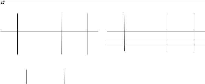
FUNCTIONAL BLOCK DIAGRAM |
PIN CONFIGURATIONS |
A |
|
|
A0 |
1 |
24 |
VCC |
|
|
|
|
|||||
(6) |
ROW |
16,384-BIT |
A1 |
2 |
23 |
A10 |
|
MEMORY |
|||||||
SELECT |
A2 |
|
|
|
|||
|
ARRAY |
3 |
22 |
A9 |
|||
|
|
||||||
|
|
|
|||||
A |
|
|
A3 |
4 |
21 |
WE |
|
I/O1 |
|
|
A4 |
5 |
20 |
OE |
|
|
|
A5 |
6 |
19 |
A8 |
||
|
INPUT |
|
|||||
|
COLUMN I/O |
A6 |
7 |
18 |
CE |
||
|
DATA |
||||||
|
CONTROL |
|
A7 |
8 |
17 |
I/O8 |
|
I/O8 |
|
|
|||||
|
|
I/O1 |
9 |
16 |
I/O7 |
||
|
|
|
|||||
|
|
COLUMN |
I/O2 |
10 |
15 |
I/O6 |
|
|
|
SELECT |
I/O3 |
11 |
14 |
I/O5 |
|
|
|
|
|||||
|
|
|
GND |
12 |
13 |
I/O4 |
WE
CE |
|
|
|
DIP (P4, D4), SOJ (J4), SOIC (S4) |
A |
(5) |
A |
DIP (P4, D4), SOJ (J3), SOIC (S4) |
|
|
TOP VIEW |
|||
|
|
|
|
TOP VIEW |
OE
See Selection Guide Page for LCC
Means Quality, Service and Speed
1Q97
47
P4C116
MAXIMUM RATINGS(1)
Symbol |
Parameter |
Value |
Unit |
|
|
|
|
VCC |
Power Supply Pin with |
–0.5 to +7 |
V |
|
Respect to GND |
|
|
|
Terminal Voltage with |
–0.5 to |
|
VTERM |
Respect to GND |
VCC +0.5 |
V |
|
(up to 7.0V) |
|
|
|
|
|
|
TA |
Operating Temperature |
–55 to +125 |
°C |
Symbol |
Parameter |
Value |
Unit |
|
|
|
|
TBIAS |
Temperature Under |
–55 to +125 |
°C |
|
Bias |
|
|
TSTG |
Storage Temperature |
–65 to +150 |
°C |
PT |
Power Dissipation |
1.0 |
W |
IOUT |
DC Output Current |
50 |
mA |
RECOMMENDED OPERATING CONDITIONS
Grade(2) |
Ambient Temp |
Gnd |
Vcc |
Commercial |
0°C to 70°C |
0V |
5.0V ±10% |
|
|
|
|
CAPACITANCES(4)
(VCC = 5.0V, TA = 25°C, f = 1.0MHz)
Symbol |
Parameter |
Conditions |
Typ. |
Unit |
|
|
|
|
|
CIN |
Input Capacitance |
VIN = 0V |
5 |
pF |
COUT |
Output Capacitance |
VOUT= 0V |
7 |
pF |
DC ELECTRICAL CHARACTERISTICS
Over recommended operating temperature and supply voltage(2)
Symbol |
Parameter |
Test Conditions |
P4C116 |
Unit |
|
|
|
|
|
||||
Min |
Max |
|
||||
|
|
|
|
|
||
|
|
|
|
|
|
|
VIH |
Input High Voltage |
|
2.2 |
VCC +0.5 |
V |
|
VIL |
Input Low Voltage |
|
–0.5(3) |
0.8 |
V |
|
VHC |
CMOS Input High Voltage |
|
VCC–0.2 |
VCC+0.5 |
V |
|
V |
CMOS Input Low Voltage |
|
–0.5(3) |
0.2 |
V |
|
LC |
|
|
|
|
|
|
VCD |
Input Clamp Diode Voltage |
VCC = Min., IIN = –18 mA |
|
–1.2 |
V |
|
VOL |
Output Low Voltage |
IOL = +8 mA, VCC = Min. |
|
0.4 |
V |
|
|
(TTL Load) |
|
|
|
|
|
|
|
|
|
|
|
|
VOH |
Output High Voltage |
IOH = –4 mA, VCC = Min. |
2.4 |
|
V |
|
|
(TTL Load) |
|
|
|
|
|
|
|
|
|
|
|
|
ILI |
Input Leakage Current |
VCC = Max., VIN = GND to VCC |
–5 |
+5 |
mA |
|
ILO |
Output Leakage Current |
VCC = Max., CS = VIH, VOUT = GND to VCC |
–5 |
+5 |
mA |
|
ICC |
Dynamic Operating |
VCC = Max., f = Max., Outputs Open |
|
130 |
mA |
|
|
Current – 10, 12 |
|
|
|
|
|
|
|
|
|
|
|
|
ICC |
Dynamic Operating |
VCC = Max., f = Max., Outputs Open |
___ |
115 |
mA |
|
|
|
|||||
|
Current – 15, 20 |
|
|
|
|
|
|
|
|
|
|
|
|
ICC |
Dynamic Operating |
VCC = Max., f = Max., Outputs Open |
___ |
100 |
mA |
|
|
|
|||||
|
Current – 25, 35 |
|
|
|
|
|
|
|
|
|
|
|
|
ISB |
Standby Power Supply |
CE ³VIH, VCC = Max., f = Max., Outputs Open |
___ |
35 |
mA |
|
|
|
|||||
|
Current (TTL Input Levels) |
|
|
|
|
|
|
|
|
|
|
|
|
ISBI |
Standby Power Supply |
CE ³VHC, VCC = Max., f = 0, Outputs Open |
___ |
17 |
mA |
|
|
|
|||||
|
Current (CMOS Input Levels) |
VIN £VLC or VIN ³ VHC |
|
|
|
|
|
|
|
|
|
|
|
48
P4C116
POWER DISSIPATION CHARACTERISTICS VS. SPEED
Symbol |
Parameter |
Temperature |
|
|
|
|
|
|
Unit |
|
Range |
–10 |
–12 |
–15 |
–20 |
–25 |
–35 |
||||
|
|
|
|
|
|
|
|
|
|
|
ICC |
Dynamic Operating Current* |
Commercial |
180 |
170 |
160 |
155 |
150 |
140 |
mA |
|
|
|
|
|
|
|
|
|
|||
Military |
N/A |
N/A |
170 |
160 |
155 |
150 |
mA |
|||
|
|
|||||||||
|
|
|
|
|
|
|
|
|
|
*VCC = 5.5V. Tested with outputs open. f = Max. Switching inputs are 0V and 3V. CE = VIL, OE = VIH.
AC ELECTRICAL CHARACTERISTICS—READ CYCLE
(VCC = 5V ± 10%, All Temperature Ranges)(2)
Sym. |
Parameter |
–10 |
–12 |
–15 |
–20 |
–25 |
–35 |
Unit |
||||
|
|
|
|
|
|
|
|
|
|
|||
|
|
Min Max |
Min |
Max |
Min |
Max |
Min |
Max |
Min |
Max |
Min Max |
|
tRC |
Read Cycle Time |
10 |
12 |
|
15 |
|
20 |
|
25 |
|
35 |
ns |
tAA |
Address Access Time |
10 |
|
12 |
|
15 |
|
20 |
|
25 |
35 |
ns |
tAC |
Chip Enable Access Time |
10 |
|
12 |
|
15 |
|
20 |
|
25 |
35 |
ns |
tOH |
Output Hold from Address Change |
2 |
2 |
|
2 |
|
2 |
|
2 |
|
2 |
ns |
tLZ |
Chip Enable to Output in Low Z |
2 |
2 |
|
2 |
|
2 |
|
3 |
|
3 |
ns |
tHZ |
Chip Disable to Output in High Z |
5 |
|
6 |
|
7 |
|
8 |
|
10 |
15 |
ns |
tOE |
Output Enable Low to Data Valid |
6 |
|
8 |
|
10 |
|
10 |
|
15 |
20 |
ns |
tOLZ |
Output Enable Low to Low Z |
0 |
0 |
|
0 |
|
0 |
|
0 |
|
0 |
ns |
tOHZ |
Output Enable High to High Z |
6 |
|
7 |
|
8 |
|
9 |
|
12 |
15 |
ns |
tPU |
Chip Enable to Power Up Time |
0 |
0 |
|
0 |
|
0 |
|
0 |
|
0 |
ns |
tPD |
Chip Disable to Power Down |
10 |
|
12 |
|
15 |
|
20 |
|
20 |
25 |
ns |
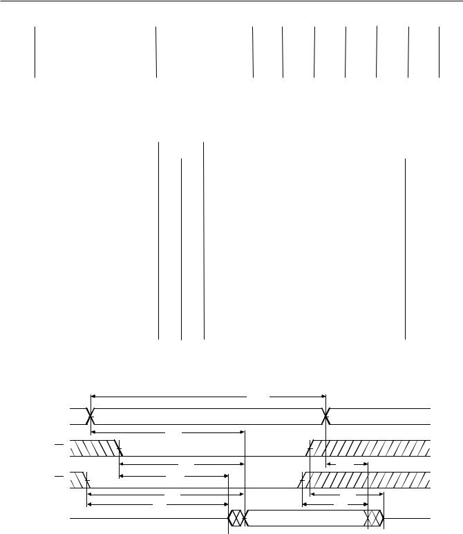
TIMING WAVEFORM OF READ CYCLE NO. 1 (OE CONTROLLED)(5)
|
(9) |
|
|
t RC |
|
ADDRESS |
|
|
t AA |
|
|
OE |
|
|
tOE |
tOH |
|
(8) |
|
|
tOLZ |
|
|
CE |
|
|
tAC |
t |
(8) |
OHZ |
||
(8) |
|
(8) |
tLZ |
t HZ |
|
DATA OUT |
|
|
Notes:
1.Stresses greater than those listed under MAXIMUM RATINGS may cause permanent damage to the device. This is a stress rating only and functional operation of the device at these or any other conditions above those indicated in the operational sections of this specification is not implied. Exposure to MAXIMUM rating conditions for extended periods may affect reliability.
2.Extended temperature operation guaranteed with 400 linear feet per minute of air flow.
3.Transient inputs with VIL and IIL not more negative than –3.0V and –100mA, respectively, are permissible for pulse widths up to 20ns.
4.This parameter is sampled and not 100% tested.
5.WE is HIGH for READ cycle.
6.CE is LOW and OE is LOW for READ cycle.
7.ADDRESS must be valid prior to, or coincident with CE transition LOW.
8.Transition is measured ± 200 mV from steady state voltage prior to change, with loading as specified in Figure 1. This parameter is sampled and not 100% tested.
9.Read Cycle Time is measured from the last valid address to the first transitioning address.
49
 Loading...