

Page 1
MM54HC182/MM74HC182
Look-Ahead Carry Generator
General Description
The MM54HC182/MM74HC182 is a high speed LOOKAHEAD CARRY GENERATOR utilize advanced silicon-gate
CMOS technology. It has the low power consumption and
high noise immunity of standard CMOS integrated circuits,
along with the ability to drive 10 LS-TTL loads.
These circuits are capable of anticipating a carry across four
binary adders or groups of adders. They are cascadable to
perform full look-ahead across n-bit adders. Carry, generate-carry, and propagate-carry functions are provided as
shown in the pin designation table.
When used in conjunction with the HC181 arithmetic logic
unit, these generators provide high-speed carry look-ahead
capability for any word length. Each HC182 generates the
look-ahead (anticipated carry) across a group of four ALU’s
and, in addition, other carry look-ahead circuits may be employed to anticipate carry across sections of four lookahead packages up to n-bits. The method of cascading circuits to perform multi-level look-ahead is illustrated under
typical application data.
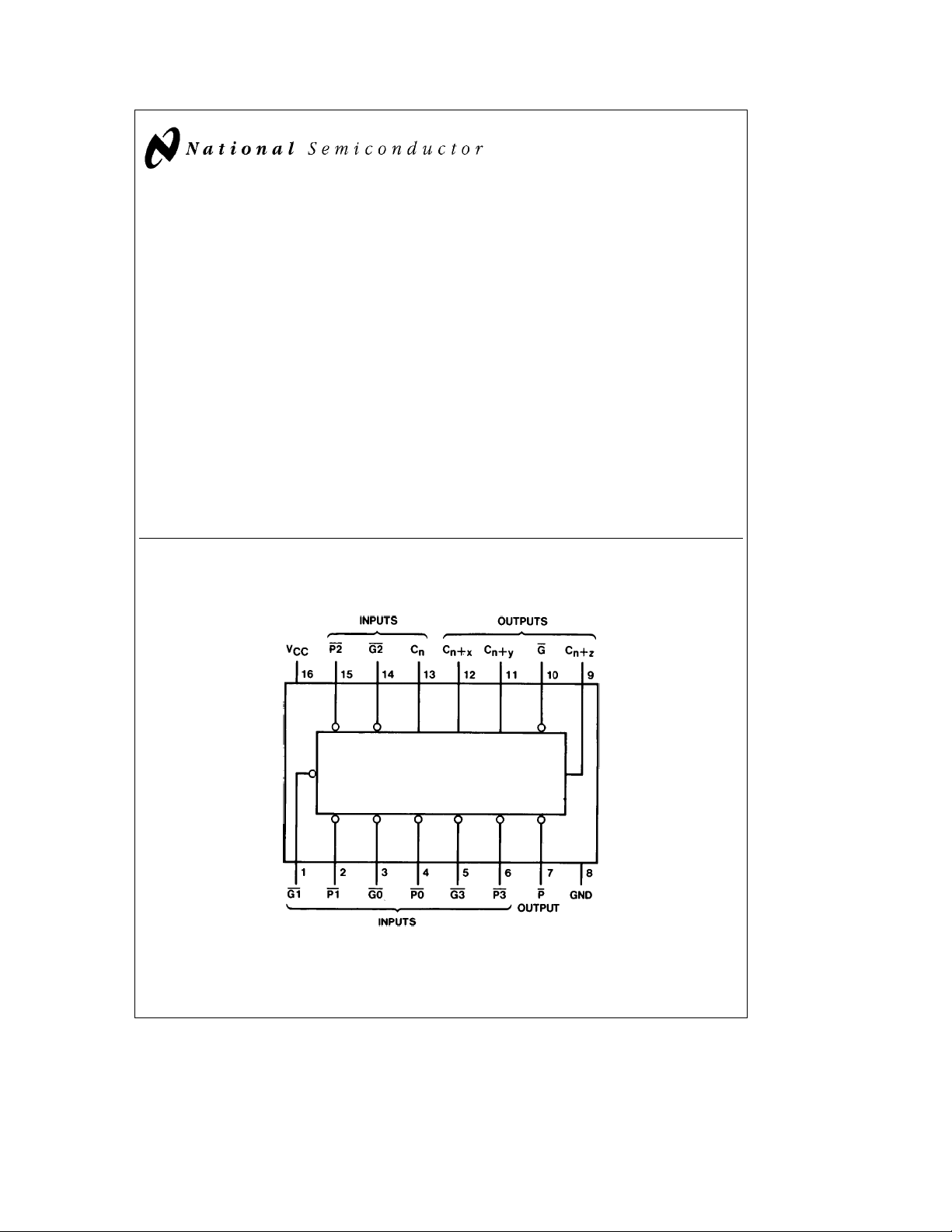
Connection Diagram
March 1988
Carry input and output of the ALU’s are in their true form,
and the carry propagate (P) and carry generate (G) are in
negated form; therefore, the carry functions (inputs, outputs,
generate, and propagate) of the look-ahead generators are
implemented in the compatible forms for direct connection
to the ALU. Reinterpretations of carry functions as explained on the HC181 data sheet are also applicable to and
compatible with the look-ahead generator.
Features
Y
TTL pinout compatible
Y
Typical propagation delay: 18 ns (clock to Q)
Y
Wide operating supply voltage range: 2– 6V
Y
Low input current: 1 mA maximum
Y
Low quiescent supply current: 80 mA maximum (74HC
Series)
Y
Fanout of 10 LS-TTL loads
MM54HC182/MM74HC182 Look-Ahead Carry Generator
Dual-In-Line Package
Top View
Order Number MM54HC182 or MM74HC182
C
1995 National Semiconductor Corporation RRD-B30M105/Printed in U. S. A.
TL/F/5321
TL/F/5321– 1
Page 2
Absolute Maximum Ratings (Notes1&2)
If Military/Aerospace specified devices are required,
please contact the National Semiconductor Sales
Office/Distributors for availability and specifications.
Supply Voltage (V
DC Input Voltage (V
DC Output Voltage (V
Clamp Diode Current (I
DC Output Current, per pin (I
DC V
or GND Current, per pin (ICC)
CC
Storage Temperature Range (T
Power Dissipation (P
(Note 3) 600 mW
CC
IN
)
)
OUT
D
)
IK,IOK
)
)
OUT
)
STG
b
b
)
b
0.5 toa7.0V
1.5 to V
CC
0.5 to V
CC
g
g
b
g
65§Ctoa150§C
a
1.5V
a
0.5V
20 mA
25 mA
50 mA
Operating Conditions
Supply Voltage (V
)26V
CC
DC Input or Output Voltage 0 V
(V
IN,VOUT
)
Operating Temp. Range (TA)
MM74HC
MM54HC
Input Rise or Fall Times
e
V
2.0V(tr,tf) 1000 ns
CC
e
V
4.5V 500 ns
CC
e
V
6.0V 400 ns
CC
Min Max Units
b
40
b
55
CC
a
85
a
125
S.O. Package only 500 mW
Lead Temperature
(T
) (Soldering 10 seconds) 260§C
L
DC Electrical Characteristics (Note 4)
Symbol Parameter Conditions V
CC
A
e
T
25§C
Typ Guaranteed Limits
V
IH
Minimum High Level 2.0V 1.5 1.5 1.5 V
Input Voltage 4.5V 3.15 3.15 3.15 V
6.0V 4.2 4.2 4.2 V
V
IL
Maximum Low Level 2.0V 0.5 0.5 0.5 V
Input Voltage** 4.5V 1.35 1.35 1.35 V
6.0V 1.8 1.8 1.8 V
V
OH
Minimum High Level V
Output Voltage
e
VIHor V
l
I
IN
OUT
IL
s
20 mA 2.0V 2.0 1.9 1.9 1.9 V
l
4.5V 4.5 4.4 4.4 4.4 V
6.0V 6.0 5.9 5.9 5.9 V
e
V
VIHor V
IN
I
l
OUT
I
l
OUT
V
OL
Maximum Low Level V
Output Voltage
l
I
IN
OUT
e
IL
s
4.0 mA 4.5V 4.2 3.98 3.84 3.7 V
l
s
5.2 mA 6.0V 5.7 5.48 5.34 5.2 V
l
VIHor V
IL
s
20 mA 2.0V 0 0.1 0.1 0.1 V
l
4.5V 0 0.1 0.1 0.1 V
6.0V 0 0.1 0.1 0.1 V
e
V
VIHor V
IN
I
l
OUT
I
l
OUT
I
IN
I
CC
Note 1: Absolute Maximum Ratings are those values beyond which damage to the device may occur.
Note 2: Unless otherwise specified all voltages are referenced to ground.
Note 3: Power Dissipation temperature derating Ð plastic ‘‘N’’ package:
Note 4: For a power supply of 5V
designing with this supply. Worst case V
I
** V
Maximum Input V
Current
Maximum Quiescent V
Supply Current I
, and IOZ) occur for CMOS at the higher voltage and so the 6.0V values should be used.
CC
limits are currently tested at 20% of VCC. The above VILspecification (30% of VCC) will be implemented no later than Q1, CY’89.
IL
e
IN
e
IN
OUT
g
10% the worst case output voltages (VOH, and VOL) occur for HC at 4.5V. Thus the 4.5V values should be used when
and VILoccur at V
IH
AC Electrical Characteristics V
IL
s
4.0 mA 4.5V 0.2 0.26 0.33 0.4 V
l
s
5.2 mA 6.0V 0.2 0.26 0.33 0.4 V
l
e
25§C, C
g
0.1
e
L
15 pF, t
VCCor GND 6.0V
VCCor GND 6.0V 8.0 80 160 mA
e
0 mA
b
12 mW/§C from 65§Cto85§C; ceramic ‘‘J’’ package:b12 mW/§C from 100§Cto125§C.
e
5.5V and 4.5V respectively. (The VIHvalue at 5.5V is 3.85V.) The worst case leakage current (IIN,
CC
e
5V, T
CC
A
Symbol Parameter Conditions Typ Guaranteed Limit Units
t
PHL,tPLH
t
PHL,tPLH
t
PHL,tPLH
Maximum Propagation Delay - Pn to P 16 24 ns
Maximum Propagation Delay - Cn to any output 18 27 ns
Maximum Propagation
Delay - Pn or Gn to any output
74HC 54HC
eb
T
40 to 85§CT
A
g
1.0
e
e
t
r
f
6ns
eb
A
23 35 ns
55 to 125§C
g
1.0 mA
V
C
§
C
§
Units
2
Page 3

AC Electrical Characteristics V
e
2.0V to 6.0V, C
CC
Symbol Parameter Conditions V
t
PHL,tPLH
t
PHL,tPLH
t
PHL,tPLH
t
TLH,tTHL
C
PD
C
IN
Note 5: CPDdetermines the no load dynamic power consumption, P
Maximum Propagation 2.0V 45 112 140 162 ns
Delay 4.5V 18 28 35 40 ns
Pn to P 6.0V 15 22 27 32 ns
Maximum Propagation 2.0V 50 125 156 182 ns
Delay 4.5V 20 30 37 44 ns
Cn to any output 6.0V 16 24 30 35 ns
Maximum Propagation 2.0V 62 155 194 225 ns
Delay 4.5V 25 37 46 54 ns
Pn or Gn to any output 6.0V 22 33 42 48 ns
Maximum Output Rise 2.0V 25 75 95 110 ns
and Fall Time 4.5V 7 15 19 22 ns
Power Dissipation Capacitance 150 pF
Maximum Input Capacitance 5 10 10 10 pF
e
CPDV
D
Logic Equations
eG0a
C
nax
C
nay
C
naz
P0 C
eG1a
eG2a
eG3a
G
n
P1 G0aP1 P0 C
P2 G1aP2 P1 P0 C
P3 G2aP3 P2 G1aP3 P2 P1 G0
PeP3 P2 P1 P0
n
n
CC
e
L
e
T
25§C
A
50 pF, t
e
e
t
6 ns (unless otherwise specified)
r
f
74HC 54HC
eb
T
40 to 85§CT
A
A
eb
55 to 125§C
Units
Typ Guaranteed Limits
6.0V 6 13 16 19 ns
2
faICCVCC, and the no load dynamic current consumption, I
CC
e
C
Y0 (X0aCn)
nax
e
C
Y1[X1aY0 (X0aCn)
nay
C
naz
eY2ÀX2a
Y1[X1aY0 (X0aCn)
or
]
e
CPDVCCfaICC.
S
Ó
]
YeY3 (X3aY2) (X3aX2aY1) (X3aX2aX1aY0)
XeX3aX2aX1aX0
FUNCTION TABLE FOR G
OUTPUT
INPUTS OUTPUT
G3G2G1G0P3P2P1 G
LXXXXXX L
XLXXLXX L
XXLXLLX L
XXXLLLL L
All other combinations H
FUNCTION TABLE FOR C
naz
OUTPUT
INPUTS OUTPUT
G2G1G0P2P1P0CnC
L X XXXXX H
XLXLXXX H
XXLLLXX H
XXXLLLH H
All other combinations L
Hehigh level Lelow level Xeirrelevant
Any inputs not shown in a given table are irrelevant with respect to that output.
naz
FUNCTION TABLE
FOR P
OUTPUT
INPUTS OUTPUT
P3P2P1P0
LLLL L
All other
combinations
P
H
G1G0P1P0CnC
LXXXX H
XLLXX H
XXLLH H
FUNCTION TABLE
FOR C
nax
INPUTS OUTPUT
G0P0CnC
LX X H
XL H H
All other
combinations
FUNCTION TABLE
FOR C
nay
OUTPUT
INPUTS OUTPUT
All other
combinations
OUTPUT
nax
L
nay
L
3
Page 4

Logic Diagram
TL/F/5321– 2
Typical Application
64-BIT ALU, FULL- CARRY LOOK AHEAD IN THREE LEVELS
A and B inputs, and F outputs of 181 are not shown. TL/F/5321– 3
4
Page 5

5
Page 6

Physical Dimensions inches (millimeters)
Order Number MM54HC182J or MM74HC182J
NS Package J16A
MM54HC182/MM74HC182 Look-Ahead Carry Generator
Order Number MM74HC182N
NS Package N16E
LIFE SUPPORT POLICY
NATIONAL’S PRODUCTS ARE NOT AUTHORIZED FOR USE AS CRITICAL COMPONENTS IN LIFE SUPPORT
DEVICES OR SYSTEMS WITHOUT THE EXPRESS WRITTEN APPROVAL OF THE PRESIDENT OF NATIONAL
SEMICONDUCTOR CORPORATION. As used herein:
1. Life support devices or systems are devices or 2. A critical component is any component of a life
systems which, (a) are intended for surgical implant support device or system whose failure to perform can
into the body, or (b) support or sustain life, and whose be reasonably expected to cause the failure of the life
failure to perform, when properly used in accordance support device or system, or to affect its safety or
with instructions for use provided in the labeling, can effectiveness.
be reasonably expected to result in a significant injury
to the user.
National Semiconductor National Semiconductor National Semiconductor National Semiconductor
Corporation Europe Hong Kong Ltd. Japan Ltd.
1111 West Bardin Road Fax: (
Arlington, TX 76017 Email: cnjwge@tevm2.nsc.com Ocean Centre, 5 Canton Rd. Fax: 81-043-299-2408
Tel: 1(800) 272-9959 Deutsch Tel: (
Fax: 1(800) 737-7018 English Tel: (
National does not assume any responsibility for use of any circuitry described, no circuit patent licenses are implied and National reserves the right at any time without notice to change said circuitry and specifications.
Fran3ais Tel: (
Italiano Tel: (
a
49) 0-180-530 85 86 13th Floor, Straight Block, Tel: 81-043-299-2309
a
49) 0-180-530 85 85 Tsimshatsui, Kowloon
a
49) 0-180-532 78 32 Hong Kong
a
49) 0-180-532 93 58 Tel: (852) 2737-1600
a
49) 0-180-534 16 80 Fax: (852) 2736-9960
 Loading...