

查询MM74HC04供应商
MM74HC04
Hex Inverte r
MM74HC04 Hex Inverter
September 1983
Revised January 2005
General Description
The MM74HC04 inverters utilize advanced silicon-gate
CMOS technology to achieve opera ting speeds similar to
LS-TTL gates with the low p ower con sumpti on of standa rd
CMOS integrated circuits.
The MM74HC04 is a triple buffered inverter. It has high
noise immunity and the ability to drive 1 0 LS-TTL loads.
The 74HC logic family is functionally as well as pin-out
compatible with the standard 74LS logic family. All inputs
are protected from damage due to static discharge by internal diode clamps to V
and ground.
CC
Features
■ Typical propagation delay: 8 ns
■ Fan out of 10 LS-TTL loads
■ Quiescent power consumption: 10
room temperature
■ Low input current: 1
µA maximum
µW maximum at
Ordering Code:
Order Number
MM74HC04M M14A 14-Lead Small Outline Integrated Circuit (SOIC), JEDEC MS-012, 0.150" Narrow
MM74HC04M_NL Pb-Free 14-Lead Small Outline Integrated Circuit (SOIC), JEDEC MS-012, 0.150" Narrow
MM74HC04SJ M14D Pb-Free 14-Lead Small Outline Package (SOP), EIAJ TYPE II, 5.3mm Wide
MM74HC04MTC MTC14 14-Lead Thin Shrink Small Outline Package (TSSOP), JEDEC MO-153, 4.4mm Wide
MM74HC04MTC_NL MTC14 Pb-Free 14-Lead Thin Shrink Small Outline Package (TSSOP), JEDEC MO-153, 4.4mm
MM74HC04N N14A 14-Lead Plastic Dual-In-Line Package (PDIP), JEDEC MS-001, 0.300" Wide
MM74HC04N_NL N14A Pb-Free 14-Lead Plastic Dual-In-Line Package (PDIP), JEDEC MS-001, 0.300" Wide
Devices also availab le in Tape and Reel. Specify by appending the suffix letter “X” to the o rdering code.
Pb-Free pac k age per JEDEC J-STD- 020B.
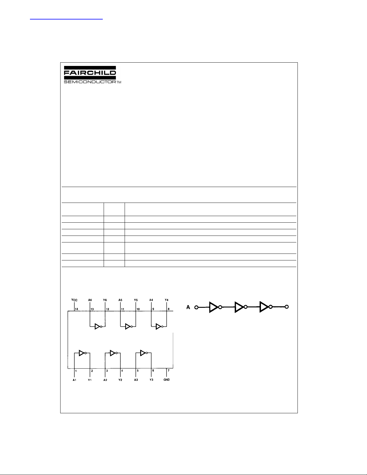
Connection Diagram
Pin Assignments for DIP, SOIC, SOP and TSSOP
Package
Number
Package Description
Wide
Logic Diagram
1 of 6 Inverters
Top View
© 2005 Fairchild Semiconductor Corporation DS005069 www.fairchildsemi.com
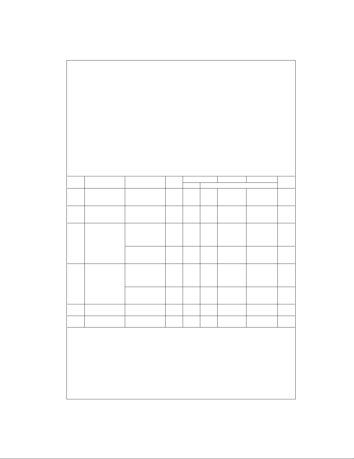
Absolute Maximum Ratings(Note 1)
(Note 2)
Supply Voltage (VCC) −0.5 to +7.0V
DC Input Voltage (V
MM74HC04
DC Output Voltage (V
Clamp Diode Current (I
DC Output Current, per pin (I
DC V
or GND Current, per pin (ICC) ±50 mA
CC
Storage Temperature Range (T
Power Dissipation (P
(Note 3) 600 mW
S.O. Package only 500 mW
Lead Temperature (T
(Soldering 10 seconds ) 260
) −1.5 to V
IN
) −0.5 to V
OUT
, IOK) ±20 mA
IK
) ±25 mA
OUT
) −65°C to +150°C
STG
)
D
)
L
CC
CC
Recommended Operating
Conditions
+1.5V
+0.5V
Supply Voltage (V
DC Input or Output Voltage 0 V
, V
(V
IN
OUT
Operating Temperature Range (T
Input Rise or Fall Times
, tf) V
(t
r
Note 1: Absolute Maximum Ratings a re those va lues beyon d which d amage to the device may occur.
Note 2: Unless otherwis e s pecified all voltages are referenced to ground.
°C
Note 3: Power Dissipa tion temper ature dera ting — plas tic “N” package: −
12 mW/°C from 65°C to 85°C.
)26V
CC
)
) −40 +85 °C
A
= 2.0V 1000 ns
CC
V
= 4.5V 500 ns
CC
V
= 6.0V 400 ns
CC
Min Max Units
DC Electrical Characteristics (Note 4)
Symbol Parameter Conditions
V
V
V
V
I
I
Minimum HIGH Level 2.0V 1.5 1.5 1.5 V
IH
Input Voltage 4.5V 3.15 3.15 3.15 V
Maximum LOW Level 2.0V 0.5 0.5 0.5 V
IL
Input Voltage 4.5V 1.35 1.35 1.35 V
Minimum HIGH Level V
OH
Output Voltage |I
Maximum LOW Level VIN = V
OL
Output Voltage |I
Maximum Input V
IN
Current
Maximum Quiescent V
CC
Supply Current I
Note 4: For a power supply of 5V ±1 0% the worst c ase ou tput volta ges (VOH, and VOL) occur for HC at 4.5V. Thus the 4. 5V valu es shoul d be use d when
designing with this supply. Worst case V
, ICC, and IOZ) occur for CMOS at the higher voltage and so the 6.0V values should be used.
(I
IN
= V
IN
IL
| ≤ 20 µA 2.0V 2.0 1.9 1.9 1.9 V
OUT
V
= V
IN
IL
|I
| ≤ 4.0 mA 4.5V 4.2 3.98 3.84 3.7 V
OUT
| ≤ 5.2 mA 6.0V 5.7 5.48 5.34 5.2 V
|I
OUT
IH
| ≤ 20 µA 2.0V 0 0.1 0.1 0.1 V
OUT
V
= V
IN
IH
|I
| ≤ 4.0 mA 4.5V 0.2 0.26 0.33 0.4 V
OUT
|I
| ≤ 5.2 mA 6.0V 0.2 0.26 0.33 0.4 V
OUT
= VCC or GND 6.0V ±0.1 ±1.0 ±1.0 µA
IN
= VCC or GND 6.0V 2.0 20 40 µA
IN
= 0 µA
OUT
and VIL occur at VCC=5.5V and 4.5V respectively. (The VIH value at 5.5V is 3. 85V.) Th e wor st c as e lea kag e cu rr ent
IH
V
CC
6.0V 4.2 4.2 4.2 V
6.0V 1.8 1.8 1.8 V
4.5V 4.5 4.4 4.4 4.4 V
6.0V 6.0 5.9 5.9 5.9 V
4.5V 0 0.1 0.1 0.1 V
6.0V 0 0.1 0.1 0.1 V
TA = 25°CTA = −40 to 85°CTA = −55 to 125°C
Typ Guaranteed Limits
CC
V
Units
www.fairchildsemi.com 2
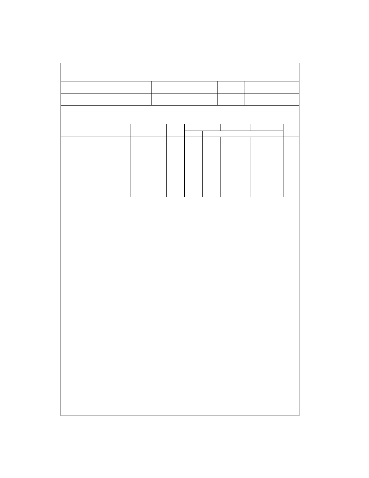
AC Electrical Characteristics
V
= 5V, TA = 25°C, CL = 15 pF, tr = t
CC
= 6 ns
f
Symbol Parameter Conditions Typ
t
, t
PHL
Maximum Propagation 8 15 ns
PLH
Delay
AC Electrical Characteristics
V
= 2.0V to 6.0V, CL = 50 pF, tr = t
CC
Symbol Parameter Conditions
t
, t
PHL
Maximum Propagation 2.0V 55 95 120 145 ns
PLH
Delay 4.5V 11 19 24 29 ns
t
, t
TLH
Maximum Output Rise 2.0V 30 75 95 110 ns
THL
and Fall Time 4.5V 8 15 19 22 ns
C
PD
Power Dissipation (per gate) 20 pF
Capacitance (Note 5)
C
IN
Maximum Input 5 10 10 10 pF
Capacitance
Note 5: CPD determines the no load dynamic power consumption, PD = CPD V
= CPDVCCf + ICC.
I
S
= 6 ns (unless otherwise specified)
f
V
CC
6.0V 9 16 20 24 ns
6.0V 7 13 16 19 ns
CC
TA = 25°CTA = −40 to 85°CTA = −55 to 125°C
Typ Guaranteed Limits
2
f + ICC VCC, and the no load dynamic current consumption,
Guaranteed
Limit
MM74HC04
Units
Units
3 www.fairchildsemi.com
 Loading...