查询MM74C908供应商
MM74C908/MM74C918 Dual CMOS 30V Relay Driver
General Description
The MM74C908 and MM74C918 are general purpose dual
high voltage drivers, each capable of sourcing a minimum of
250 mA at V
The MM74C908 and MM74C918 consist of two CMOS
NAND gates driving an emitter follower Darlington output to
achieve high current drive and high voltage capabilities. In
the ‘‘OFF’’ state the outputs can withstand a maximum of
b
30V across the device. These CMOS drivers are useful in
interfacing normal CMOS voltage levels to driving relays,
regulators, lamps, etc.
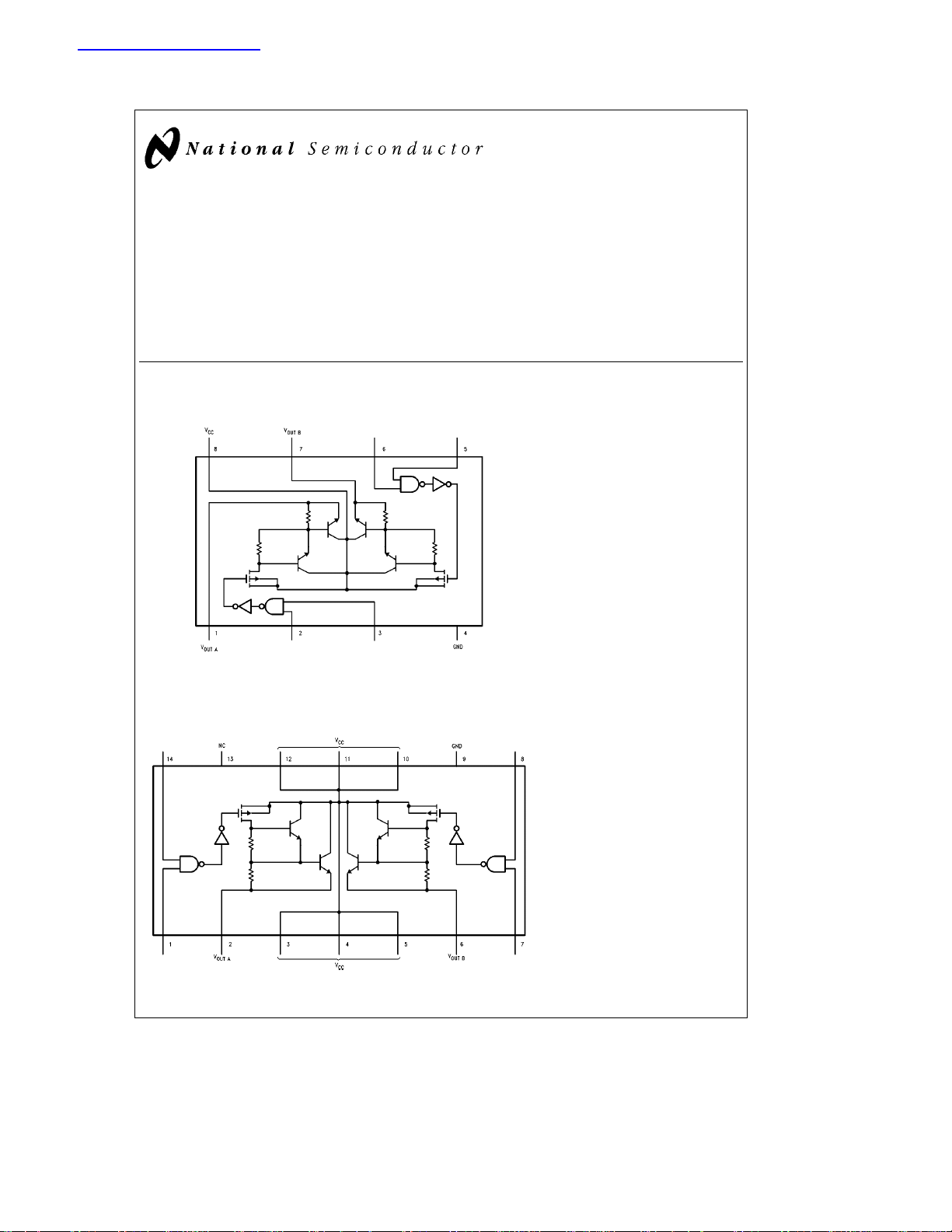
Connection Diagrams
OUT
e
V
b
3V, and T
CC
Dual-In-Line Package
MM74C908
MM74C908/MM74C918 Dual CMOS 30V Relay Driver
November 1990
Features
Y
Wide supply voltage range 3V to 18V
Y
e
65§C.
J
High noise immunity 0.45 VCC(typ.)
Y
Low output ‘‘ON’’ resistance 8X (typ.)
Y
High voltage
Y
High current 250 mA
b
30V
Order Number MM74C908
Top View
TL/F/5912– 1
Dual-In-Line Package
MM74C918
Order Number MM74C918
Top View
TL/F/5912– 2
TRI-STATEÉis a registered trademark of National Semiconductor Corporation.
C
1995 National Semiconductor Corporation RRD-B30M105/Printed in U. S. A.
TL/F/5912

Absolute Maximum Ratings (Note 1)
If Military/Aerospace specified devices are required,
please contact the National Semiconductor Sales
Office/Distributors for availability and specifications.
Voltage at any Input Pin
b
0.3V to V
CC
a
0.3V
Voltage at any Output Pin 32V
Operating Temperature Range
MM74C908/MM74C918
b
40§Ctoa85§C
Operating V
Absolute Maximum V
I
SOURCE
Storage Temperature Range (TS)
Lead Temperature (TL)
(Soldering, 10 seconds) 260
Power Dissipation (PD) Refer to Maximum Power
Range 4V to 18V
CC
CC
b
65§Ctoa150§C
Dissipation vs Ambient
Temperature Graph
500 mA
DC Electrical Characteristics Min/Max limits apply across temperature range, unless otherwise noted
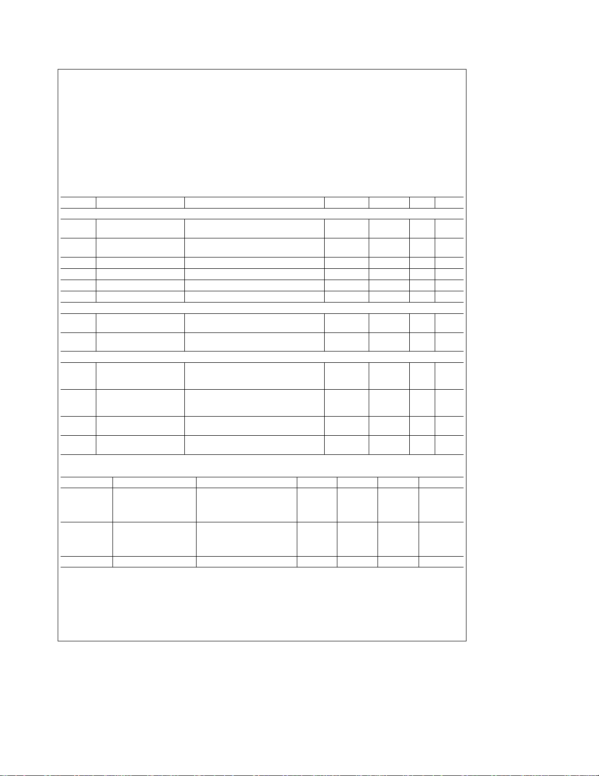
Symbol Parameter Conditions Min Typ Max Units
CMOS TO CMOS
V
V
I
IN(1)
I
IN(0)
I
CC
IN(1)
IN(0)
Logical ‘‘1’’ Input Voltage V
Logical ‘‘0’’ Input Voltage V
Logical ‘‘1’’ Input Current V
Logical ‘‘0’’ Input Current V
Supply Current V
Output ‘‘OFF’’ Voltage V
CMOS/LPTTL INTERFACE
V
V
IN(1)
IN(0)
Logical ‘‘1’’ Input Voltage
MM74C908/MM74C918 V
Logical ‘‘0’’ Input Voltage
MM74C908/MM74C918 V
OUTPUT DRIVE
V
R
i
OUT
ON
JA
Output Voltage I
Output Resistance I
Output Resistance 0.55 0.80 %/§C
Coefficient
Thermal Resistance (Note 3) 100 110§C/W
MM74C908/MM74C918 (Note 3) 45 55
e
5V 3.5 V
CC
e
10V 8.0 V
V
CC
e
5V 1.5 V
CC
e
10V 2.0 V
V
CC
OUT
I
OUT
I
OUT
OUT
I
OUT
I
OUT
CC
CC
CC
IN
CC
CC
e
e
e
e
e
e
eb
eb
eb
eb
eb
eb
VCC,I
e
15V, V
15V, V
15V 0.005 1.0 mA
IN
e
0V
IN
b
1.0
b
0.005 mA
15V, Outputs Open Circuit 0.05 15 mA
eb
OUT
200 mA
4.75V V
CC
b
b
30 V
1.5 V
4.75V 0.8 V
t
300 mA, V
250 mA, V
175 mA, V
300 mA, V
250 mA, V
175 mA, V
CC
CC
CC
CC
CC
CC
t
t
t
t
t
e
5V, T
25§CV
J
e
5V, T
65§CV
J
e
5V, T
150§CV
J
e
5V, T
25§C 6.0 9.0 X
J
e
5V, T
65§C 7.5 12 X
J
e
5V, T
150§C1018X
J
CC
CC
CC
b
2.7 V
b
3.0 V
b
3.15 V
b
1.8 V
CC
b
1.9 V
CC
b
2.0 V
CC
19V
C/W
§
C
§
AC Electrical Characteristics*
Symbol Parameter Conditions Min Typ Max Units
t
pd1
t
pd0
C
IN
*AC Parameters are guaranteed by DC correlated testing.
Note 1: ‘‘Absolute Maximum Ratings’’ are those values beyond which the safety of the device cannot be guaranteed. Except for ‘‘Operating Temperature Range’’
they are not meant to imply that the devices should be operated at these limits. The table of ‘‘Electrical Characteristics’’ provides conditions for actual device
operation.
Note 2: Capacitance is guaranteed by periodic testing.
Note 3: i
JA
Propagation Delay V
to a Logical ‘‘1’’ C
Propagation Delay V
to a Logic ‘‘0’’ C
Input Capacitance (Note 2) 5.0 pF
measured in free air with device soldered into printed circuit board.
e
CC
e
L
e
V
CC
e
C
L
e
CC
e
L
e
V
CC
e
C
L
5V, R
50 pF, T
10V, R
50 pF, T
5V, R
50 pF, T
10V, R
50 pF, T
e
50X,
L
e
25§C
A
e
50X,
L
e
25§C
A
e
50X,
L
e
25§C
A
e
50X,
L
e
25§C
A
150 300 ns
65 120 ns
2.0 10 ms
4.0 20 ms
2
 Loading...