

现货库存、技术资料、百科信息、热点资讯,精彩尽在鼎好!
LM1578A/LM2578A/LM3578A
Switching Regulator
LM1578A/LM2578A/LM3578A Switching Regulator
April 1998
General Description
The LM1578A is a switching regulator which can easily be
set up for such DC-to-DC voltage conversion circuits as the
buck, boost, and inverting configurations. The LM1578A features a unique comparator input stage which not only has
separate pins for both the inverting and non-inverting inputs,
but also provides an internal 1.0V reference to each input,
thereby simplifying circuit design and p.c. board layout. The
output can switch up to 750 mA and has output pins for its
collector and emitter to promote design flexibility.An external
current limit terminal may be referenced to either the ground
or the V
tion, the LM1578A has an on board oscillator,which sets the
switching frequency with a single external capacitor from
Hz to 100 kHz (typical).
The LM1578A is an improved version of the LM1578, offering higher maximum ratings for the total supply voltage and
output transistor emitter and collector voltages.
terminal, depending upon the application. In addi-
in
<
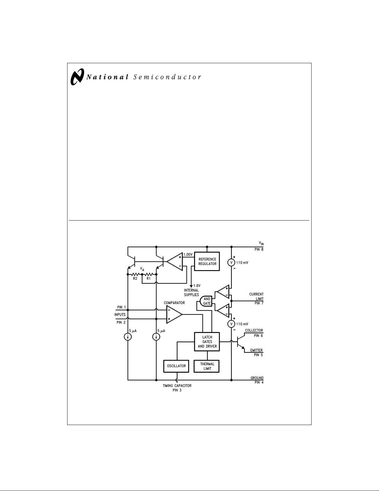
Functional Diagram
Features
n Inverting and non-inverting feedback inputs
n 1.0V reference at inputs
n Operates from supply voltages of 2V to 40V
n Output current up to 750 mA, saturation less than 0.9V
n Current limit and thermal shut down
n Duty cycle up to 90
%
Applications
n Switching regulators in buck, boost, inverting, and
single-ended transformer configurations
n Motor speed control
1
n Lamp flasher
DS008711-1
© 1998 National Semiconductor Corporation DS008711 www.national.com
Absolute Maximum Ratings (Note 1)
If Military/Aerospace specified devices are required,
please contact the National Semiconductor Sales Office/
Distributors for availability and specifications.
Total Supply Voltage 50V
Collector Output to Ground −0.3V to +50V
Emitter Output to Ground (Note 2) −1V to +50V
Power Dissipation (Note 3) Internally limited
Output Current 750 mA
Storage Temperature −65˚C to +150˚C
Lead Temperature
(soldering, 10 seconds) 260˚C
Maximum Junction Temperature 150˚C
ESD Tolerance (Note 4) 2 kV
Operating Ratings
Ambient Temperature Range
LM1578A −55˚C ≤ T
LM2578A −40˚C ≤ T
LM3578A 0˚C ≤ T
Junction Temperature Range
LM1578A −55˚C ≤ T
LM2578A −40˚C ≤ T
LM3578A 0˚C ≤ T
≤+125˚C
A
≤+85˚C
A
≤+70˚C
A
≤+150˚C
J
≤+125˚C
J
≤+125˚C
J
Electrical Characteristics
These specifications apply for 2V ≤ VIN≤ 40V (2.2V ≤ VIN≤ 40V for TJ≤ −25˚C), timing capacitor C
duty cycle ≤ 75%, unless otherwise specified. Values in standard typeface are for T
operation over the specified operating junction temperature range.
=
25˚C; values in boldface type apply for
J
LM1578A LM2578A/
Symbol Parameter Conditions Typical Limit LM3578A Units
(Note 5) (Note 6)
(Note 11)
OSCILLATOR
f
OSC
∆f
OSC
Frequency 20 kHz
/∆T Frequency Drift with −0.13
Temperature
Amplitude 550 mV
REFERENCE/COMPARATOR (Note 8)
=
V
R
Input Reference I
Voltage I
=
I
0 mA and 1.0 V
1
2
=
=
±
I
1
2
1%(Note 9) 1.035/1.050 1.050/1.070 V (max)
1mA
0.965/0.950 0.950/0.930 V (min)
=
∆V
I
/∆V
R
Input Reference Volt- I
IN
age Line Regulation I
INV
Inverting Input I
=
I
0 mA and 0.003
1
2
=
=
±
I
1
2
=
=
I
1
2
1%(Note 9) 0.01/0.02 0.01/0.02%/V (max)
1mA
0 mA, duty cycle=25
%
0.5 µA
Current
Level Shift Accuracy Level Shift Current=1 mA 1.0
∆V
/∆t Input Reference 100 ppm/1000h
R
Voltage Long Term
Stability
OUTPUT
V
(sat) Collector Saturation I
C
=
750 mA pulsed, Emitter 0.7 V
C
Voltage grounded 0.85/1.2 0.90/1.2 V (max)
V
(sat) Emitter Saturation I
E
Voltage V
I
CES
Collector Leakage V
=
80 mA pulsed, 1.4 V
O
=
=
V
IN
IN
40V 1.6/2.1 1.7/2.0 V (max)
C
=
=
V
40V, Emitter 0.1 µA
CE
Current grounded, Output OFF 50/100 200/250 µA (max)
BV
CEO(SUS)
Collector-Emitter I
SUST
=
0.2A (pulsed), V
=
060 V
IN
Sustaining Voltage 50 50 V (min)
=
3900 pF, and 25%≤
T
Limit
(Note 7)
22.4 24 kHz (max)
17.6 16 kHz (min)
%
/˚C
%
/V
%
5/8 10/13
%
(max)
p-p
www.national.com 2
Electrical Characteristics (Continued)
These specifications apply for 2V ≤ VIN≤ 40V (2.2V ≤ VIN≤ 40V for TJ≤ −25˚C), timing capacitor C
duty cycle ≤ 75%, unless otherwise specified. Values in standard typeface are for T
operation over the specified operating junction temperature range.
=
25˚C; values in boldface type apply for
J
LM1578A LM2578A/
Symbol Parameter Conditions Typical Limit LM3578A Units
(Note 5) (Note 6)
(Note 11)
CURRENT LIMIT
V
Sense Voltage Referred to VINor Ground 110 mV
CL
Shutdown Level (Note 10) 95 80 mV (min)
∆V
/∆T Sense Voltage 0.3
CL
Temperature Drift
I
CL
Sense Bias Current Referred to V
IN
4.0 µA
Referred to ground 0.4 µA
DEVICE POWER CONSUMPTION
I
S
Supply Current Output OFF, V
=
0V 2.0 mA
E
3.0/3.3 3.5/4.0 mA (max)
0V
=
750 mA pulsed, 14 mA
C
Output ON, I
=
V
Note 1: Absolute Maximum Ratings indicate limits beyond which damage to the device may occur. DC andAC electrical specifications do not apply when operating
the device beyond its rated operating conditions.
Note 2: For T
Note 3: At elevated temperatures, devices must be derated based on package thermal resistance. The device in the TO-99 package must be derated at 150˚C/W,
junction to ambient, or 45˚C/W,junction tocase. Thedevice inthe 8-pinDIP must be deratedat 95˚C/W,junction to ambient. The device in the surface-mount package
must be derated at 150˚C/W, junction-to-ambient.
Note 4: Human body model, 1.5 kΩ in series with 100 pF.
Note 5: Typical values are for T
Note 6: All limits guaranteed and 100%production tested at room temperature (standard type face) and at temperatureextremes (bold type face). All limits are used
to calculate Average Outgoing Quality Level (AOQL).
Note 7: All limits guaranteed at room temperature (standard type face) and at temperature extremes (bold type face). Room temperature limits are 100%production
tested. Limits at temperatureextremes are guaranteed via correlationusing standard Statistical Quality Control (SQC) methods.All limitsare used to calculateAOQL.
Note 8: Input terminals are protected from accidental shorts to ground but if external voltages higher than the reference voltage are applied, excessive current will
flow and should be limited to less than 5 mA.
Note 9: I
Note 10: Connection ofa 10 kΩ resistor frompin 1 to pin 4will drive the duty cycleto its maximum, typically 90%.Applying the minimum Current Limit Sense Voltage
to pin 7 will not reduce the duty cycle to less than 50%. Applying the maximum Current Limit Sense Voltage to pin 7 is certain to reduce the duty cycle below 50%.
Increasing this voltage by 15 mV may be required to reduce the duty cycle to 0%, when the Collector output swing is 40V or greater (see Ground-Referred Current
Limit Sense Voltage typical curve).
Note 11: Amilitary RETS specification is available on request.At the time of printing, the LM1578ARETS spec complied with the boldface limits in this column. The
LM1578AH may also be procured as a Standard Military Drawing.
≥ 100˚C, the Emitter pin voltage should not be driven more than 0.6V below ground (see Application Information).
J
=
25˚C and represent the most likely parametric norm.
J
and I2are the external sink currents at the inputs (refer to Test Circuit).
1
E
=
3900 pF, and 25%≤
T
Limit
(Note 7)
140 160 mV (max)
%
/˚C
3 www.national.com
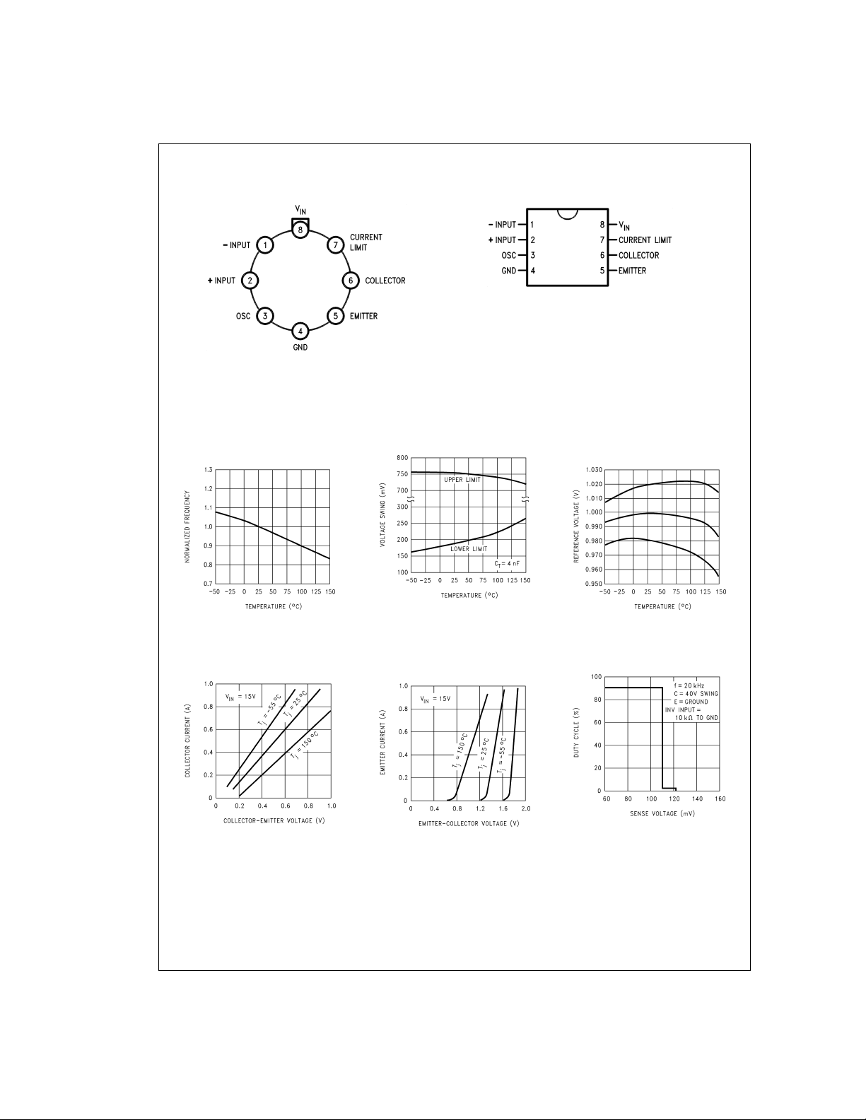
Connection Diagram and Ordering Information
Metal Can
DS008711-28
Top View
Order Number LM1578AH/883 or SMD
#
5962-8958602
See NS Package Number H08C
Typical Performance Characteristics
Oscillator Frequency Change
with Temperature
Oscillator Voltage Swing
Dual-In-Line Package
DS008711-29
Order Number LM3578AM, LM2578AN or LM3578AN
See NS Package Number M08A or N08E
Input Reference Voltage
Drift with Temperature
DS008711-32
Collector Saturation Voltage
(Sinking Current,
Emitter Grounded)
DS008711-35
www.national.com 4
Emitter Saturation Voltage
(Sourcing Current,
Collector at V
)
in
DS008711-33
DS008711-36
DS008711-34
Ground Referred
Current Limit Sense Voltage
DS008711-37
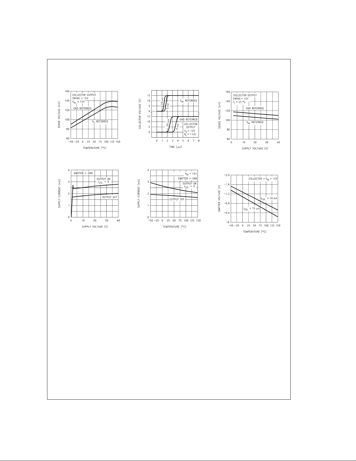
Typical Performance Characteristics (Continued)
Current Limit Sense Voltage
Drift with Temperature
Supply Current
Test Circuit
*
DS008711-38
DS008711-41
Current Limit Response Time
for Various Over Drives
Supply Current
Parameter tests can be made using the test circuit shown.
Select the desired V
adjustable power supplies. A digital volt meter with an input
, collector voltage and duty cycle with
in
resistance greater than 100 MΩ should be used to measure
the following:
Input Reference Voltage to Ground; S1 in either position.
Level Shift Accuracy (%)=(T
=
1mA
Input Current (mA)=(1V − T
0 mA.
(V)/1V) x 100%;S1atI
P3
(V))/1 MΩ:S1atI
p3
Oscillator parameters can be measured at T
quency counter or an oscilloscope.
p4
=
1
=
I
1
2
using a fre-
Current Limit Sense Voltage
vs Supply Voltage
DS008711-39
Collector Current with
Emitter Output Below Ground
DS008711-42
The Current Limit Sense Voltageis measured by connecting
an adjustable 0-to-1V floating power supply inseries with the
current limit terminal and referring it to either the ground or
the V
terminal. Set the duty cycle to 90%and monitor test
in
point T
until the LM1578A’s duty cycle just reaches 0%. This voltage
while adjusting the floating power supply voltage
P5
is the Current Limit Sense Voltage.
The Supply Current should be measured with the duty cycle
I
at 0%and S1 in the I
2
*
=
LM1578A specifications are measured using automated
test equipment. This circuit is provided for the customer’s
=
1
=
I
0 mA position.
2
convenience when checking parameters. Due to possible
variations in testing conditions, the measured values from
these testing procedures may not match those of the factory.
DS008711-40
DS008711-43
5 www.national.com
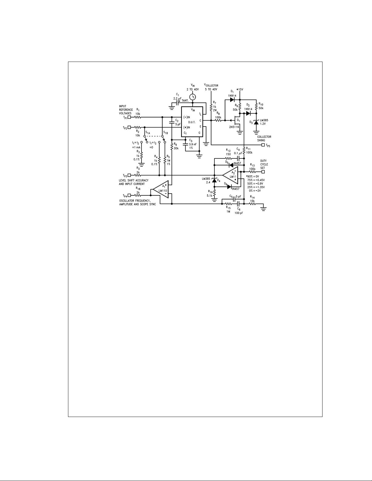
Test Circuit
*
(Continued)
Op amp supplies are±15V
DVM input resistance
*
LM1578 max duty cycle is 90
>
100 MΩ
%
Definition of Terms
Input Reference Voltage: The voltage (referred to ground)
that must be applied to either the inverting or non-inverting
input to cause the regulator switch to change state (ON or
OFF).
Input Reference Current: The current that must be drawn
from either the inverting or non-inverting input to cause the
regulator switch to change state (ON or OFF).
Input Level Shift Accuracy: This specification determines
the output voltagetoleranceof a regulator whose output control depends on drawing equal currents from the inverting
and non-inverting inputs (see the Inverting Regulator of
ure 21
, and the RS-232 Line Driver Power Supply of
23
).
Level Shift Accuracy is tested by using two equal-value resistors to draw current from the inverting and non-inverting
input terminals, then measuring the percentage difference in
the voltages across the resistors that produces a controlled
duty cycle at the switch output.
Collector Saturation Voltage: With the inverting input terminal grounded thru a 10 kΩ resistor and the output transistor’s emitter connected to ground, the Collector SaturationVoltage is the collector-to-emitter voltage for a given
collector current.
Emitter Saturation Voltage: With the inverting input terminal grounded thru a 10kΩresistor and the output transistor’s
collector connected to V
the collector-to-emitter voltage for a given emitter current.
, the Emitter Saturation Voltage is
in
Collector Emitter Sustaining Voltage: The
collector-emitter breakdown voltage of the output transistor,
measured at a specified current.
Fig-
Figure
DS008711-3
Current Limit Sense Voltage: The voltage at the Current
Limit pin, referred to either the supply or the ground terminal,
which (via logic circuitry) will cause the output transistor to
turn OFF and resets cycle-by-cycle at the oscillator frequency.
Current Limit Sense Current: The bias current for the Current Limit terminal with the applied voltage equal to the Current Limit Sense Voltage.
Supply Current: The IC power supply current, excluding the
current drawn through the output transistor, with the oscillator operating.
Functional Description
The LM1578A is a pulse-width modulator designed for use
as a switching regulator controller. It may also be used in
other applications which require controlled pulse-width voltage drive.
Acontrol signal, usually representing output voltage, fed into
the LM1578A’s comparator is compared with an
internally-generated reference. The resulting error signal
and the oscillator’s output are fed to a logic network which
determines when the output transistor will be turned ON or
OFF. The following isa brief description of the subsections of
the LM1578A.
COMPARATOR INPUT STAGE
The LM1578A’s comparator input stage is unique in that
both the inverting and non-inverting inputs are available to
the user, and both contain a 1.0V reference. This is accomplished as follows: A 1.0V reference is fed into a modified
voltage follower circuit (see FUNCTIONAL DIAGRAM).
When both input pins are open, no current flows through R1
www.national.com 6

Functional Description (Continued)
and R2.Thus, both inputs to the comparator will have the potential of the 1.0V reference, V
ample the non-inverting input, is pulled ∆V away from V
current of ∆V/R1 will flow through R1. This same current
flows through R2, and the comparator sees a total voltage of
2∆V between its inputs. The high gain of the system, through
feedback, will correct for this imbalance and return both inputs to the 1.0V level.
This unusual comparator input stage increases circuit flexibility, while minimizing the total number of external components required for a voltage regulator system. The inverting
switching regulator configuration, for example, can be set up
without having to use an external op amp for feedback polarity reversal (see TYPICALAPPLICATIONS).
OSCILLATOR
The LM1578A provides an on-board oscillator which can be
adjusted up to 100 kHz. Itsfrequency is set by a single external capacitor, C
equation
=
f
8x10
OSC
, as shown in
1
−5
/C
1
The oscillator provides a blanking pulse to limit maximum
duty cycle to 90%, and a reset pulse to the internal circuitry.
. When one input, for ex-
A
Figure 1
, and follows the
,a
A
Applications Information
CURRENT LIMIT
As mentioned in the functional description, the current limit
terminal may be referenced to either the V
terminal. Resistor R3 converts the current to be sensed into
a voltage for current limit detection.
FIGURE 2. Current Limit, Ground Referred
or the ground
in
DS008711-15
DS008711-4
FIGURE 1. Value of Timing Capacitor vs
Oscillator Frequency
OUTPUT TRANSISTOR
The output transistor is capable of delivering up to 750 mA
with a saturation voltage of less than 0.9V. (see
Saturation Voltage
and
Emitter Saturation Voltage
Collector
curves).
The emitter must not be pulled more than 1V below ground
(this limit is 0.6V for T
ternal transistor must be used to develop negative output
≥ 100˚C). Because of this limit, an ex-
J
voltages (see the Inverting Regulator Typical Application).
Other configurations may need protection against violation
of this limit (see the Emitter Output section of the Applications Information).
CURRENT LIMIT
The LM1578A’s current limit may be referenced to either the
ground or the V
sis.
pins, and operates on a cycle-by-cycle ba-
in
The current limit section consists of two comparators: one
with its non-inverting input referenced to a voltage 110 mV
below V
110mV above ground (see FUNCTIONAL DIAGRAM). The
, the other with its inverting input referenced
in
current limit is activated whenever the current limit terminal
is pulled 110 mV away from either V
or ground.
in
DS008711-16
FIGURE 3. Current Limit, VinReferred
CURRENT LIMIT TRANSIENT SUPPRESSION
When noise spikes and switching transients interfere with
proper current limit operation, R1 and C1 act together as a
low pass filter to control the current limit circuitry’s response
time.
Because the sense current of the currentlimit terminal varies
according to where it is referenced, R1 should be less
than 2 kΩ when referenced to ground, and less than 100Ω
when referenced to V
.
in
DS008711-17
FIGURE 4. Current Limit Transient Suppressor,
Ground Referred
7 www.national.com

Applications Information (Continued)
DS008711-18
FIGURE 5. Current Limit Transient Suppressor,
C.L. SENSE VOLTAGE MULTIPLICATION
When a larger sense resistor value is desired, the voltage divider network, consisting of R1 and R2, may be used. This
effectively multiplies the sense voltage by (1 + R1/R2). Also,
R1 can be replaced by a diode to increase current limit
sense voltage to about 800 mV (diode V
V
in
Referred
+ 110 mV).
f
non-inverting input than is sunk by the parallel combination
of R1 and R2 at the inverting terminal. R3 should be one-fifth
of the value of R1 and R2 in parallel.
DS008711-22
FIGURE 8. Under-Voltage Lockout
MAXIMUM DUTY CYCLE LIMITING
The maximum duty cycle can be externally limited by adjusting the charge to discharge ratio of the oscillator capacitor
with a single external resistor. Typical values are 50 µA for
the charge current, 450 µA for the discharge current, and a
voltage swing from 200 mV to 750 mV. Therefore, R1 is selected for the desired charging and discharging slopes and
C1 is readjusted to set the oscillator frequency.
DS008711-19
FIGURE 6. Current Limit Sense Voltage Multiplication,
Ground Referred
DS008711-20
FIGURE 7. Current Limit Sense Voltage Multiplication,
V
Referred
in
UNDER-VOLTAGE LOCKOUT
Under-voltage lockout is accomplished with few external
components. When V
breakdown voltage, the output transistor is turned off. This
becomes lower than the zener
in
occurs because diode D1 will then become forward biased,
allowing resistor R3 to sink a greater current from the
www.national.com 8
DS008711-21
FIGURE 9. Maximum Duty Cycle Limiting
DUTY CYCLE ADJUSTMENT
When manual or mechanical selection of the output transistor’s duty cycle is needed, the cirucit shown below may be
used. The output will turn on with the beginning of each oscillator cycle and turn off when the current sunk by R2 and
R3 from the non-inverting terminal becomes greater than the
current sunk from the inverting terminal.
With the resistor values as shown, R3 can be used to adjust
the duty cycle from 0%to 90%.
When the sum of R2 and R3 is twice the value of R1, the
duty cycle will be about 50%. C1 may be a large electrolytic
capacitor to lower the oscillator frequency below 1 Hz.

Applications Information (Continued)
DS008711-23
FIGURE 10. Duty Cycle Adjustment
REMOTE SHUTDOWN
The LM1578A may be remotely shutdown by sinking a
greater current from the non-inverting input than from the inverting input.This may be accomplished by selecting resistor
R3 to be approximately one-half the value of R1 and R2 in
parallel.
DS008711-30
FIGURE 12. D1 Prevents Output Transistor from
Improperly Turning ON due to D2’s Forward Voltage
SYNCHRONIZING DEVICES
When several devices are to be operated at once, their oscillators may be synchronized by the application of an external
signal. This drive signal should be a pulse waveform with a
minimum pulse width of 2 µs. and an amplitude from 1.5V to
2.0V. The signal source must be capable of 1.) driving capacitive loads and 2.) delivering up to 500 µA for each
LM1578A.
Capacitors C1 thru CN are to be selected for a 20%slower
frequency than the synchronization frequency.
DS008711-24
FIGURE 11. Shutdown Occurs when VLis High
EMITTER OUTPUT
When the LM1578A output transistor is in the OFF state, if
the Emitter output swings below the ground pin voltage, the
output transistor will turn ON because its base is clamped
near ground. The
low Ground
Collector Current with Emitter Output Be-
curve shows the amount of Collector current
drawn in this mode, vs temperature and Emitter voltage.
When the Collector-Emitter voltage is high, this current will
cause high power dissipation in the output transistor and
should be avoided.
This situation can occur in the high-current high-voltage
buck application if the Emitter output is used and the catch
diode’s forward voltage drop is greater than 0.6V. A
fast-recovery diode can be added in series with the Emitter
output to counter the forward voltage drop of the catch diode
(see
Figure 2
). For better efficiency of a high output current
buck regulator,an external PNP transistor should be used as
shown in
Figure 16
.
DS008711-25
FIGURE 13. Synchronizing Devices
Typical Applications
The LM1578A may be operated in either the continuous or
the discontinuous conduction mode. The following applications (except for the Buck-Boost Regulator) are designed for
continuous conduction operation. That is, the inductor current is not allowed to fall to zero. This mode of operation has
higher efficiency and lower EMI characteristics than the discontinuous mode.
BUCK REGULATOR
The buck configuration is used to step an input voltage down
to a lower level. Transistor Q1 in
DC voltage into a squarewave.Thissquarewave is then converted back into a DC voltage of lower magnitude by the low
pass filter consisting of L1 and C1. The duty cycle, D, of the
squarewave relates theoutputvoltage to the input voltage by
the following equation:
=
V
out
9 www.national.com
DxV
=
in
x(ton)/(ton+t
V
in
Figure 14
).
off
chops the input

Typical Applications (Continued)
DS008711-5
FIGURE 14. Basic Buck Regulator
Figure 15
rent, I
20%of I
ciency of 75%, a load regulationof 30 mV (70 mA to350 mA)
and a line regulation of 10 mV (12 ≤ V
Component values are selected as follows:
R1=(V
R3=V/I
R3=0.15Ω
where:
V is the current limit sense voltage, 0.11V
I
sw(max)
transistor.
L1 is the inductor and may be found from the inductance cal-
culation chart (
Given V
Note that since the circuit will become discontinuous at 20
of I
70 mA.
Step 1: Calculate the maximum DC current through the inductor, I
top of the chart and show that I
configuration. Thus, I
is a 15V to 5V buck regulator with an output cur-
, of 350 mA. The circuit becomes discontinuous at
o
, has 10 mV of output voltage ripple, an effi-
o(max)
≤ 18V).
in
− 1) x R2 where R2=10 kΩ
o
sw(max)
is the maximum allowable current thru the output
Figure 16
=
350 mA
50 kHz
) as follows:
=
L(max)
o(max)
L(max)
350 mA.
=
.
I
o(max)
for the buck
=
15V
in
=
5V
V
o
I
o(max)
=
f
OSC
Discontinuous at 20%of I
, the load current must not be allowed to fall below
o(max)
. The necessary equations are indicated at the
L(max)
Step 2: Calculate the inductor Volts-sec product, E-T
cording to the equations given from the chart. For the Buck:
=
E-T
op
=
(15 − 5) (5/15) (1000/50)
=
66V-µs.
with the oscillator frequency, f
V
V
V
I
o
f
osc
R1=40 kΩ D1=1N5818
R2=10 kΩ
)(Vo/Vin) (1000/f
(V
in−Vo
, expressed in kHz.
osc
=
15V R3=0.15Ω
in
=
5V C1=1820 pF
o
=
10 mV C2=220 µF
ripple
=
350 mA C3=20 pF
=
50 kHz L1=470 µH
)
osc
DS008711-6
, ac-
op
FIGURE 15. Buck or Step-Down Regulator
Step 3: Using the graph with axis labeled “Discontinuous At
%
” and “I
I
OUT
maximum inductor current, I
discontinuity percentage.
” find the point where the desired
L(max, DC)
L(max, DC)
intercepts the desired
In this example, the point of interest is where the 0.35A line
%
intersects with the20%line. Thisis nearly the midpoint of the
horizontal axis.
Step 4: This last step is merely the translation of the point
found in Step 3 to the graph directly below it. This is accomplished by moving straight down the page to the point which
intercepts the desired E-T
66V-µs and the desired inductor value is 470 µH. Since this
. For this example, E-Topis
op
example was for 20%discontinuity, the bottom chart could
have been used directly, as noted in step 3 of the chart
instructions.
www.national.com 10

Typical Applications (Continued)
DS008711-31
FIGURE 16. DC/DC Inductance Calculator
11 www.national.com

Typical Applications (Continued)
For a full line of standard inductor values, contact Pulse Engineering (San Diego, Calif.) regarding their PE526XX series, or A. I. E. Magnetics (Nashville, Tenn.).
A more precise inductance value may be calculated for the
Buck, Boost and Inverting Regulators as follows:
BUCK
L=V
o(Vin−Vo
BOOST
L=V
in(Vo−Vin
INVERT
L=V
in|Vo
where ∆I
usually chosen based onthe minimum load current expected
of the circuit. For the buck regulator, since the inductor current I
L
=
∆I
2
L
=
∆I
140 mA for this circuit. ∆I
L
=
∆I
2
L
where the Discontinuity Factor is the ratio of the minimum
load current to the maximum load current. For this example,
the Discontinuity Factor is 0.2.
The remainder of the components of
as follows:
C1 is the timing capacitor found in
C2 ≥ V
)/(∆ILVinf
)/(∆ILf
|/[∆IL(Vin+|Vo|)f
is the current ripple through the inductor. ∆ILis
L
oscVo
)
osc
)
]
osc
equals the load current IO,
I
•
O(min)
(Discontinuity Factor)•I
•
o(Vin−Vo
)/(8f
osc
can also be interpreted as
L
L
Figure 15
VinV
ripple
Figure 1
L1)
2
are chosen
.
where V
is the peak-to-peak output voltage ripple.
ripple
C3 is necessary for continuous operation and is generally in
the 10 pF to 30 pF range.
D1 should be a Schottky type diode, such as the 1N5818 or
1N5819.
BUCK WITH BOOSTED OUTPUT CURRENT
For applications requiring a large output current, an external
transistor may be used as shown in
Figure 17
. This circuit
steps a 15V supply down to 5V with 1.5A of output current.
The output ripple is 50 mV, with an efficiency of 80%, a load
regulation of 40 mV (150 mA to 1.5A), and a line regulation
of 20 mV (12V ≤ V
≤ 18V).
in
Component values are selected as outlined for the buck
regulator with a discontinuity factor of 10%, with the addition
of R4 and R5:
R4=10V
R5=(Vin−V−V
BE1Bf/Ip
BE1−Vsat)Bf
/(I
L(max, DC)+IR4
)
where:
is the VBEof transistor Q1.
V
BE1
is the saturation voltage of the LM1578A output transis-
V
sat
tor.
V is the current limit sense voltage.
B
is the forced current gain of transistor Q1 (B
f
ure 17
).
=
=
I
L(max, DC)
/R4
V
BE1
+ 0.5∆I
L
I
R4
I
p
=
Fig-
30 for
f
=
15V R4=200Ω
V
in
=
5V R5=330Ω
V
o
=
50 mV C1=1820 pF
V
ripple
=
1.5A C2=330 µF
I
o
=
50 kHz C3=20 pF
f
osc
R1=40 kΩ L1=220 µH
R2=10 kΩ D1=1N5819
R3=0.05Ω Q1 = D45
FIGURE 17. Buck Converter with Boosted Output Current
BOOST REGULATOR
The boost regulator converts a low input voltage into a
higher output voltage. The basic configuration is shown in
Figure 18
. Energy is stored in the inductor while the transistor is on and then transferred with the input voltage to the
output capacitor for filtering when the transistor is off. Thus,
=
V
V
o
in+Vin(ton/toff
www.national.com 12
).
DS008711-8

Typical Applications (Continued)
DS008711-9
FIGURE 18. Basic Boost Regulator
The circuit of
Figure 19
ply with 150 mA of output current, a load regulation of 14 mV
(30 mA to 140 mA), and a line regulation of 35 mV (4.5V ≤
V
≤ 8.5V).
in
=
V
5V R4=200 kΩ
in
=
15V C1=1820 pF
V
o
=
V
ripple
=
140 mA C3=20 pF
I
o
=
50 kHz C4=0.0022 µF
f
osc
R1=140 kΩ L1=330 µH
R2=10 kΩ D1=1N5818
R3=0.15Ω
FIGURE 19. Boost or Step-Up Regulator
R1=(V
R3=V/(I
− 1) R2 where R2=10 kΩ.
o
L(max, DC)
where:
=
∆I
2(I
L
LOAD(min)
is 200 mA in this example.
∆I
L
converts a 5V supply into a 15V sup-
DS008711-11
10 mV C2=470 µF
+ 0.5 ∆IL)
)(Vo/Vin)
R4, C3 and C4 are necessary for continuous operation and
are typically 220 kΩ, 20 pF, and 0.0022 µF respectively.
C1 is the timing capacitor found in
C2 ≥ I
o(Vo−Vin
Figure 1
)/(f
oscVoVripple
.
).
D1 is a Schottky type diode such as a IN5818 or IN5819.
L1 is found as described in the buck converter section, using
the inductance chart for
Figure 16
for the boost configuration
and 20%discontinuity.
INVERTING REGULATOR
Figure 20
shows the basic configuration for an inverting
regulator. The input voltage is of a positive polarity, but the
output is negative. The output may be less than, equal to, or
greater in magnitude than the input. The relationship between the magnitude of the input voltage and the output voltage is V
=
x(ton/t
V
o
in
).
off
DS008711-10
FIGURE 20. Basic Inverting Regulator
Figure 21
shows an LM1578A configured as a 5V to −15V
polarity inverter with an output current of 300 mA, a load
regulation of 44 mV (60 mA to 300 mA) and a line regulation
of 50 mV (4.5V ≤ V
R1=(|V
R4=10V
≤ 8.5V).
in
| +1) R2 where R2=10 kΩ.
o
R3=V/(I
BE1Bf
L(max, DC)
/(I
L (max, DC)
+ 0.5 ∆IL).
+ 0.5 ∆IL)
where:
V, V
Boosted Output Current” section.
∆I
L
, and Bfare defined in the “Buck Converter with
BE1,Vsat
=
2(I
LOAD(min)
)(Vin+|Vo|)/V
IN
R5 is defined in the “Buck with Boosted Output Current” section.
R6 serves the same purpose as R4 in the Boost Regulator
circuit and is typically 220 kΩ.
C1, C3 and C4 are defined in the “Boost Regulator” section.
C2 ≥ I
o|Vo
|/[f
(|Vo|+Vin)V
osc
ripple
]
L1 is found as outlined in the section on buck converters, using the inductance chart of
Figure 16
for the invert configura-
tion and 20%discontinuity.
13 www.national.com

Typical Applications (Continued)
=
V
5V R4=190Ω
in
=
−15V R5=82Ω
V
o
=
5mV R6=220 kΩ
V
ripple
=
300 mA C1=1820 pF
I
o
=
60 mA C2=1000 µF
I
min
=
50 kHz C3=20 pF
f
osc
R1=160 kΩ C4=0.0022 µF
R2=10 kΩ L1=150 µH
R3=0.01Ω D1=1N5818
FIGURE 21. Inverting Regulator
BUCK-BOOST REGULATOR
Figure 22
The Buck-Boost Regulator, shown in
voltage up or down, depending upon whether or not the desired output voltage is greater or less than the input voltage.
In this case, the output voltage is 12V with an input voltage
from 9V to 15V. The circuit exhibits an efficiencyof 75%, with
a load regulation of 60 mV (10 mA to 100 mA) and a line
regulation of 52 mV.
R1=(V
− 1) R2 where R2=10 kΩ
o
R3=V/0. 75A
R4, C1, C3 and C4 are defined in the “Boost Regulator” sec-
tion.
D1 and D2 are Schottky type diodes such as the 1N5818 or
1N5819.
where:
is the forward voltage drop of the diodes.
V
d
is the saturation voltage of the LM1578A output transis-
V
sat
tor.
V
is the saturation voltage of transistor Q1.
sat1
L1 ≥ (V
in−Vsat−Vsat1
where:
, may step a
)(ton/Ip)
DS008711-12
RS-232 LINE DRIVER POWER SUPPLY
Figure 23
The power supply, shown in
, operates from an in-
put voltage as low as 4.2V (5V nominal),anddelivers an out-
±
put of
12V at±40 mA with better than 70%efficiency.The
circuit provides a load regulation of
100%of full load) and a line regulation of
±
150 mV (from 10%to
±
10 mV.Other notable features include a cycle-by-cycle current limit and an
output voltage ripple of less than 40 mVp-p.
A unique feature of this circuit is its use of feedback from
both outputs. This dual feedback configuration results in a
sharing of the output voltage regulation by each output so
that neither side becomes unbalanced as in single feedback
systems. In addition, since both sides are regulated, it is not
necessary to use a linear regulator for output regulation.
The feedback resistors, R2 and R3, may be selected as follows by assuming a value of 10 kΩ for R1;
R2=(V
R3=(|V
− 1V)/45.8 µA=240 kΩ
o
| +1V)/54.2 µA=240 kΩ
o
Actually, the currents used to program the values for the
feedback resistors may vary from 40 µAto 60 µA, as long as
their sum is equal to the 100 µA necessary to establish the
1V threshold across R1. Ideally, these currents should be
equal (50 µA each) for optimal control. However, as was
done here, theymay be mismatched in order to use standard
resistor values.Thisresults in a slight mismatch of regulation
between the two outputs.
The current limit resistor, R4, is selected by dividing the current limit threshold voltage by the maximum peak current
level in the output switch. For our purposes R4=110mV/
750 mA=0.15Ω. A value of 0.1Ω was used.
www.national.com 14

Typical Applications (Continued)
9V ≤ Vin≤ 15V R5=270
=
12V C1=1820 pF
V
o
= 100 mA C2=220 µF
I
o
=
50 mV C3=20 pF
V
ripple
=
50 kHz C4=0.0022 µF
f
osc
R1=110k L1=220 µH
R2=10k D1, D2=1N5819
R3=0.15 Q1=D44
R4=220k
FIGURE 22. Buck-Boost Regulator
DS008711-13
DS008711-14
=
V
5V R4=0.15Ω
in
±
12V C1=820 pF
V
o
=
±
40 mA C2=10 pF
I
o
=
80 kHz C3=220 µF
f
osc
R1=10 kΩ D1, D2, D3=1N5819
R2=240 kΩ T1=PE-64287
R3=240 kΩ
FIGURE 23. RS-232 Line Driver Power Supply
Capacitor C1 sets the oscillator frequency and is selected
Figure 1
from
.
Capacitor C2 serves as a compensation capacitor for synchronous operation and a value of10 to 50 pF should be sufficient for most applications.
A minimum value for an ideal output capacitor C3, could be
calculated as C=I
the transistor on time (typically 0.4/f
peak-to-peak output voltage ripple. A larger output capacitor
xt/∆V where Iois the load current, t is
o
), and ∆Visthe
osc
than this theoretical value should be used since electrolytics
have poor high frequency performance. Experience has
shown that a value from 5 to 10 times the calculated value
should be used.
For good efficiency,the diodes must have a low forward voltage drop and be fast switching. 1N5819 Schottky diodes
work well.
Transformerselection should be picked for an output transistor “on” time of 0.4/f
enough to prevent the output transistor switch from ramping
, and a primary inductance high
osc
higher than the transistor’s rating of 750 mA. Pulse Engineering (San Diego, Calif.) and Renco Electronics, Inc.
(Deer Park, N.Y.) can provide further assistance in selecting
the proper transformer for a specific application need. The
transformer used in
Figure 23
was a Pulse Engineering
PE-64287.
15 www.national.com

16

Physical Dimensions inches (millimeters) unless otherwise noted
Order Number LM1578AH/883 or SMD
Metal Can Package (H)
NS Package Number H08C
Plastic Surface-Mount Package (M)
Order Number LM3578AM
NS Package Number M08A
#
5962-8958602
17 www.national.com

Physical Dimensions inches (millimeters) unless otherwise noted (Continued)
Molded Dual-In-Line Package (N)
Order Number LM2578AN or LM3578AN
LM1578A/LM2578A/LM3578A Switching Regulator
NS Package Number N08E
LIFE SUPPORT POLICY
NATIONAL’S PRODUCTS ARE NOT AUTHORIZED FOR USE AS CRITICAL COMPONENTS IN LIFE SUPPORT DEVICES OR SYSTEMS WITHOUT THE EXPRESS WRITTEN APPROVAL OF THE PRESIDENT OF NATIONAL SEMICONDUCTOR CORPORATION. As used herein:
1. Life support devices or systems are devices or systems which, (a) are intended for surgical implant into
the body, or (b) support or sustain life, and whose failure to perform when properly used in accordance
2. A critical component in any component of a life support
device or system whose failure to perform can be reasonably expected to cause the failure of the life support
device or system, or to affect its safety or effectiveness.
with instructions for use provided in the labeling, can
be reasonably expected to result in a significant injury
to the user.
National Semiconductor
Corporation
Americas
Tel: 1-800-272-9959
Fax: 1-800-737-7018
Email: support@nsc.com
www.national.com
National does not assume any responsibility for use of any circuitry described, no circuit patent licenses are implied and National reserves the right at any time without notice to change said circuitry and specifications.
National Semiconductor
Europe
Fax: +49 (0) 1 80-530 85 86
Email: europe.support@nsc.com
Deutsch Tel: +49 (0) 1 80-530 85 85
English Tel: +49 (0) 1 80-532 78 32
Français Tel: +49 (0) 1 80-532 93 58
Italiano Tel: +49 (0) 1 80-534 16 80
National Semiconductor
Asia Pacific Customer
Response Group
Tel: 65-2544466
Fax: 65-2504466
Email: sea.support@nsc.com
National Semiconductor
Japan Ltd.
Tel: 81-3-5620-6175
Fax: 81-3-5620-6179
 Loading...