

Page 1
TL/H/7912
LM1872 Radio Control Receiver/Decoder
February 1989
LM1872 Radio Control Receiver/Decoder
General Description
The LM1872 is a complete RF receiver/decoder for radio
control applications. The device is well suited for use at either 27 MHz, 49 MHz or 72 MHz in controlling various toys
or hobby craft such as cars, boats, tanks, trucks, robots,
planes, and trains. The crystal controlled superhet design
offers both good sensitivity and selectivity. When operated
in conjunction with the companion transmitter, LM1871, it
provides four independent information channels. Two of
these channels are analog pulse width modulated (PWM)
types, while the other two are simple ON/OFF digital channels with 100 mA drive capability. Either channel type can
be converted to the other form through simple external circuitry such that up to 4 analog or up to 4 digital channels
could be created. Few external parts are required to complement the self-contained device which includes local oscillator, mixer, IF detector, AGC, sync output drivers, and all
decoder logic on-chip.
Features
Y
Four independent information channels; two analog and
two digital
Y
Completely self-contained
Y
Minimum of external parts
Y
Operation from 50 kHz to 72 MHz
Y
Highly selective and sensitive superhet design
Y
Operates from four 1.5V cells
Y
Excellent supply noise rejection
Y
100 mA digital output drivers
Y
Crystal controlled
Y
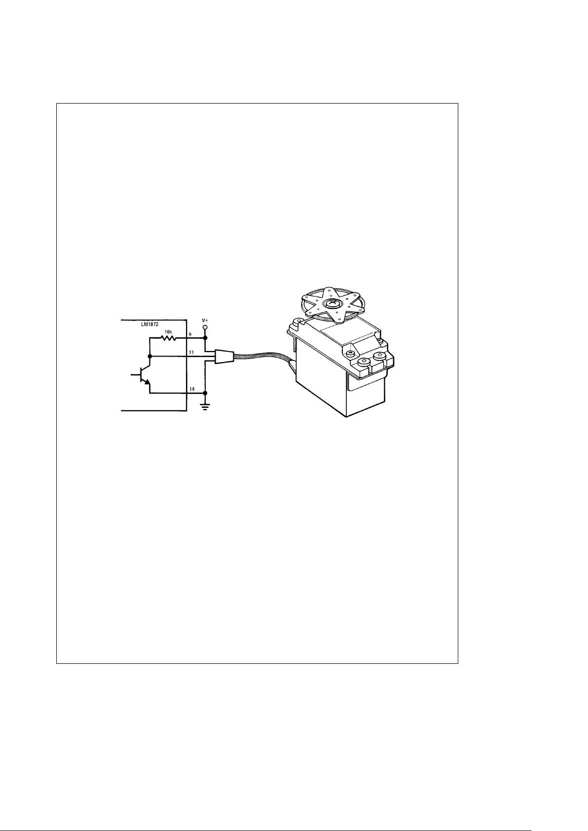
Interfaces directly with standard hobby servos
Applications
Y
Toys and hobby craft
Y
Energy saving, remotely switched lighting systems
Y
Burgler alarms
Y
Industrial and consumer remote data links
Y
IR data links
Y
Remote slide projector control
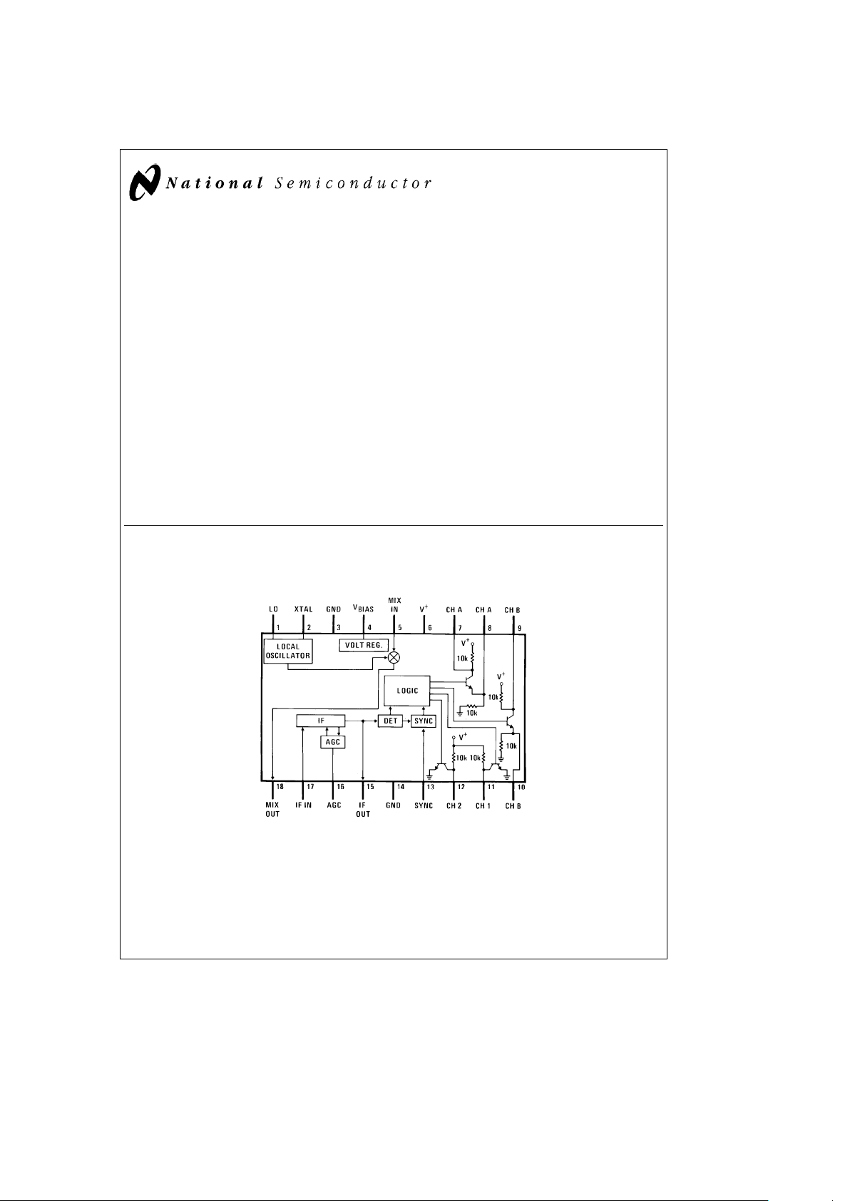
Circuit Block and Connection Diagram
Dual-In-Line Package
TL/H/7912– 1
Bottom View
Order Number LM1872N
See NS Package Number N18A
C
1995 National Semiconductor Corporation RRD-B30M115/Printed in U. S. A.
Page 2
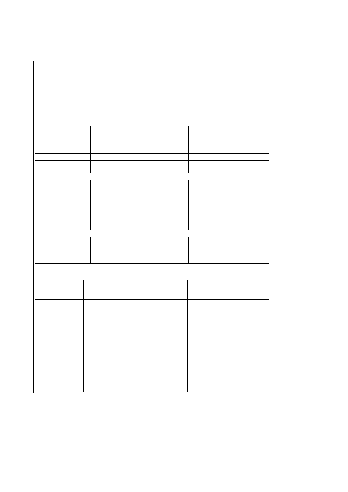
Absolute Maximum Ratings
If Military/Aerospace specified devices are required,
please contact the National Semiconductor Sales
Office/Distributors for availability and specifications.
Supply Voltage 7V
Package Dissipation (Note 2) 1600 mW
Voltage
@
Pin 7, 8, 9, 10, 11 or 12 V
a
Operating Temperature Range
b
25§Ctoa85§C
Storage Temperature Range
b
65§Ctoa150§C
Lead Temperature (Soldering, 10 sec.) 260§C
DC Electrical Characteristics
V
a
e
6V, T
A
e
25§C, Test Circuit of
Figure 1
,f
L0
e
49.890 MHz, f
IF
e
455 kHz unless otherwise specified
Parameter Conditions Min Typ Max Units
Supply Voltage Functional for V
IN
e
100 mV 2.5 6 7 V
Supply Current CHA&BOff 9 13 18 mA
CHA&BOn
27 mA
V
BIAS
@
Pin 4 1.85 2.1 2.35 V
Sync Timer Threshold
@
Pin 13, Going from
V
a
/2b0.4 Va/2 Va/2a0.3 V
Low to High Voltage
DIGITAL CHANNELS A AND B
Saturation Voltage
@
Pins7&9,R
L
e
100X 0.4 0.7 V
Saturation Resistance
@
Pins7&9 7 X
Source Current
@
Pins 8 & 10,
100 mA
V
Pin 8 & Pin 10
s
1V
Collector Pull-Up Pin7&Pin9toV
a
51020kX
Resistance
Emitter Pull-Down Pin 8 & Pin 10 to GND
51020kX
Resistance
ANALOG CHANNELS 1 AND 2
Saturation Voltage
@
Pins 11 & 12, R
L
e
2kX 0.45 0.7 V
Saturation Resistance
@
Pins 11 & 12 160 X
Collector Pull-Up Pin 11 & Pin 12 to V
a
51020kX
Resistance
AC Electrical Characteristics
Parameter Conditions Min Typ Max Units
RF Sensitivity For ‘‘Solid’’ Decoded Outputs
22 39 mV
(Note 1)
RF Sensitivity Circuit of
Figure 5
@
49 MHz
with Antenna Simulation 12 mV
Network of
Figure 6
Voltage Gain Pin 5 to Pin 15 58 dB
PSRR of RF Sensitivity 3VsV
a
s
6V
b
1%D/V
BW 3 dB Down@Pin 15 3.2 kHz
Noise Referred to Input, Pin 5, V
IN
e
0 0.35 mVrms
Referred to IF, Pin 15, V
IN
e
0 0.28 mVrms
AGC Threshold Onset of AGC Relative to
88 mV
RF Input, VIN,@Pin 5
Relative to IF Output@Pin 15 V
a
a
0.07 V
a
a
0.100 V
a
a
0.13 V
Mixer Conversion From Pin 5 to Pin 18
@
1 MHz 2.9 4.0 6.9 mmhos
Transconductance
@
27 MHz 3.7 mmhos
@
49 MHz 3.5 mmhos
2
Page 3

AC Electrical Characteristics (Continued)
Parameter Conditions Min Typ Max Units
Mixer Input Impedance Pin 5 to Pin 4@49 MHz
20 kX
a
5pF
(See Curves)
Mixer Output Impedance Pin 18 to GND 250 kX
IF Transconductance Pin 17 to Pin 15 (AGC Off)@455 kHz 2.6 4.1 5.6 mmhos
IF Input Impedance Pin 17 to GND 5500 X
IF Output Impedance Pin 15 to GND (AGC Off) 800 kX
(AGC On) 2 MX
IF Carrier Level
@
Pin 15, V
IN
e
100 mV
70 mVrms
(AGC On)
Detector Threshold Relative to RF Input,
20 mV
V
IN
,@Pin 5
Relative to IF Output@Pin 15 V
a
a
0.015 V
a
a
0.025 V
a
a
0.040 V
Analog Pulse Width Ratio of Received Pulse Width
Accuracy
@
Pins 11 & 12 to Transmitted
0.95 1.0 1.05 ms/ms
Pulse Width
@
Pin 5 for
V
IN
e
100 mV
Note 1: The criteria for the outputs to be considered ‘‘solid’’ are as follows:
DIGITAL: In order to check the decoding section, four RF frames are inputted in sequence with the proper codes to exercise all four possible logical
output combinations at pins 7 and 9. For each frame the proper output logic state must exist.
ANALOG: Each analog pulse width (measured at pins 11 & 12) in any of the above four successive frames must not vary more than
g
5% from the pulse
widths obtained for V
IN
e
100 mV.
Note 2: For operation in ambient temperatures above 25
§
C, the device must be derated based on a 150§C maximum junction temperature and a package
thermal resistance of 75
§
C/W, junction to ambient.
Typical Performance Characteristics
Supply Voltage
Supply Current vs
Voltage vs Load Current
Analog Channel Output
vs Load Current
Collector Output Voltage
Digital Channel
Sensitivity vs Supply Voltage vs Input Frequency
Mixer Transconductance (g
m
)
Input Signal Level
IF Output Signal Level vs RF
TL/H/7912– 2
3
Page 4

Typical Performance Characteristics (Continued)
IF Bandpass Response vs Frequency
Resistance and Capacitance
Equivalent Mixer Input Shunt
vs RF Input Level
Receiver AM Rejection
TL/H/7912– 3
Test Circuit
TL/H/7912– 4
Bottom View
L1eToko* 10k type (KEN-4028 DZ); 6T T2eToko* 10 EZC type (RMC 402503 NO), Que110
T1
e
Toko* 10 EZC type (RMC 202313 NO), Que110 Pin 1 –2, 98T; pin 2– 3, 66T
Pin 1 –2, 131T; pin 2– 3, 33T Pin 1 –3, 164T; pin 4– 6, 8T
Pin 1 –3, 164T; pin 4– 6, 5T
*Toko America
1250 Feehanville Drive
Mount Prospect, IL 60056
(312) 297-0070
FIGURE 1. Test Circuit
4
Page 5
Circuit Description
The following discussion is best understood by referring to
Figures 2, 3, 4,
and5.
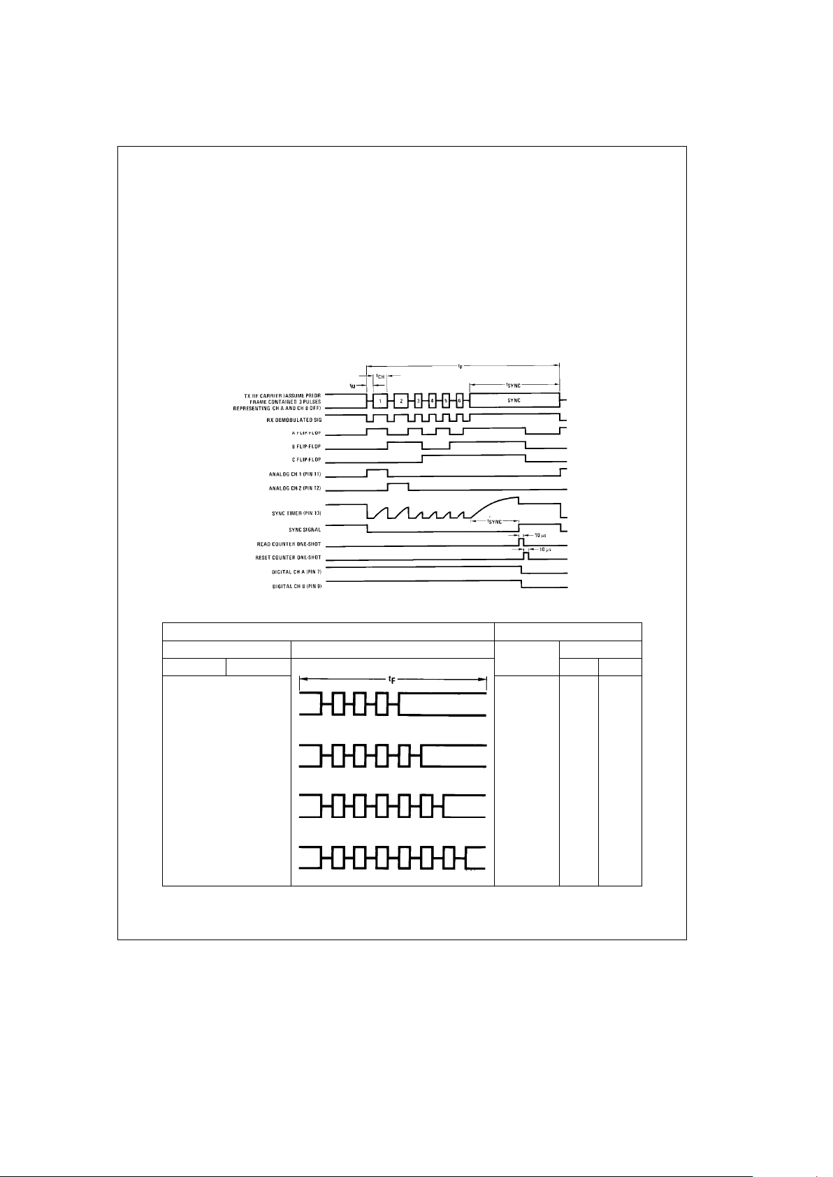
SYSTEM ENCODING AND DECODING SCHEME
For the transfer of analog information, the LM1871/LM1872
system uses conventional pulse width modulation (PWM). In
applying this technique, the RF carrier is interrupted for
short fixed intervals (t
M
in
Figure 2
) with each interval fol-
lowed by variable width pulses (t
CH
) so as to define multiple
variable time spans (t
M
a
tCH) occurring in serial fashion.
Synchronization is accomplished by allowing one of the
transmitted variable pulse widths (t
SYNC
) to exceed the du-
ration (t’
SYNC
) of a receiver-based timer, thus allowing the
receiver to recognize this pulse for synchronization purposes. Taken in sequence, this collection of pulses constitutes
a single frame period (t
F
).
The LM1871 transmitter is equipped to transmit up to
six
channels which the companion LM1872 receiver uses to
derive 2 analog and 2 digital channels. The receiver decodes the demodulated RF waveform from the transmitter
by negative edge triggering a cascade of three binary dividers called the A, B, and C toggle flip-flops (
Figure 4
). By
‘‘examining’’ all three flip-flop outputs simultaneously, up to
6 unique channel time intervals could be identified and recovered. Only the first two channels are actually decoded
however and outputted by the receiver, the rest being used
for identification of two digital (ON/OFF) channels. In passing digital information, a pulse count modulation scheme is
used whereby different quantities of channel pulses are
transmitted by varying the number of fixed width channels
following the two variable width analog channels 1 and 2
(see
Figure 3
).
TL/H/7912– 5
FIGURE 2. RX Timing Waveforms
LM1871 TX LM1872 RX
Pin Conditions Transmitted Waveform Binary Digital Outputs
Pin 5 (CH A) Pin 6 (CH B)
Pulse Count
CH A CH B
OPEN OPEN 100 OFF OFF
TL/H/7912– 6
GND OPEN 101 ON OFF
TL/H/7912– 7
OPEN GND 110 OFF ON
TL/H/7912– 8
GND GND 111 ON ON
TL/H/7912– 9
FIGURE 3. Digital Channel Encoding and Decoding via Pulse Count Modulation
5
Page 6

Circuit Description (Continued)
TL/H/7912– 10
*External parts
²
Depending on layout, a small capacitance (10 –47 pF)
may be required across pins 2 and 3 to ensure
oscillator start up.
FIGURE 4. Simplified Schematic Diagram
6
Page 7
Circuit Description (Continued)
Thus either 3, 4, 5, or 6 channels are transmitted to represent the four possible codes that two digital channels represent. The receiver intrinsically counts channels with its decoder flip-flops by responding to the negative edges of the
demodulated RF waveform of which there is always one
more than the number of channels. The two LSBs of the
binary count are read, latched, and fed to the output drivers
which comprise digital channels A and B.
RECEIVER SECTION
The receiver circuit is a simple, single conversion design
with AGC which mixes down to 455 kHz and provides
58 dB of gain using the suggested transformers in
Figure 5
.
The active digital detector provides an additional 30 dB gain
over a silicon diode resulting in an overall system gain of
88 dB. More or less gain can be obtained by using different
transformers. The frequency range of operation extends
from 50 kHz to 72 MHz encompassing a wide range of allocated frequency bands.
The short (1
Ê
to 2Ê) vertical whip antenna that is typically
used has a very low radiation resistance (0.5X to 4X) and
approximately 3 pF to 5 pF of capacitance. This antenna is
coupled to the mixer through a high Q tank consisting of C3
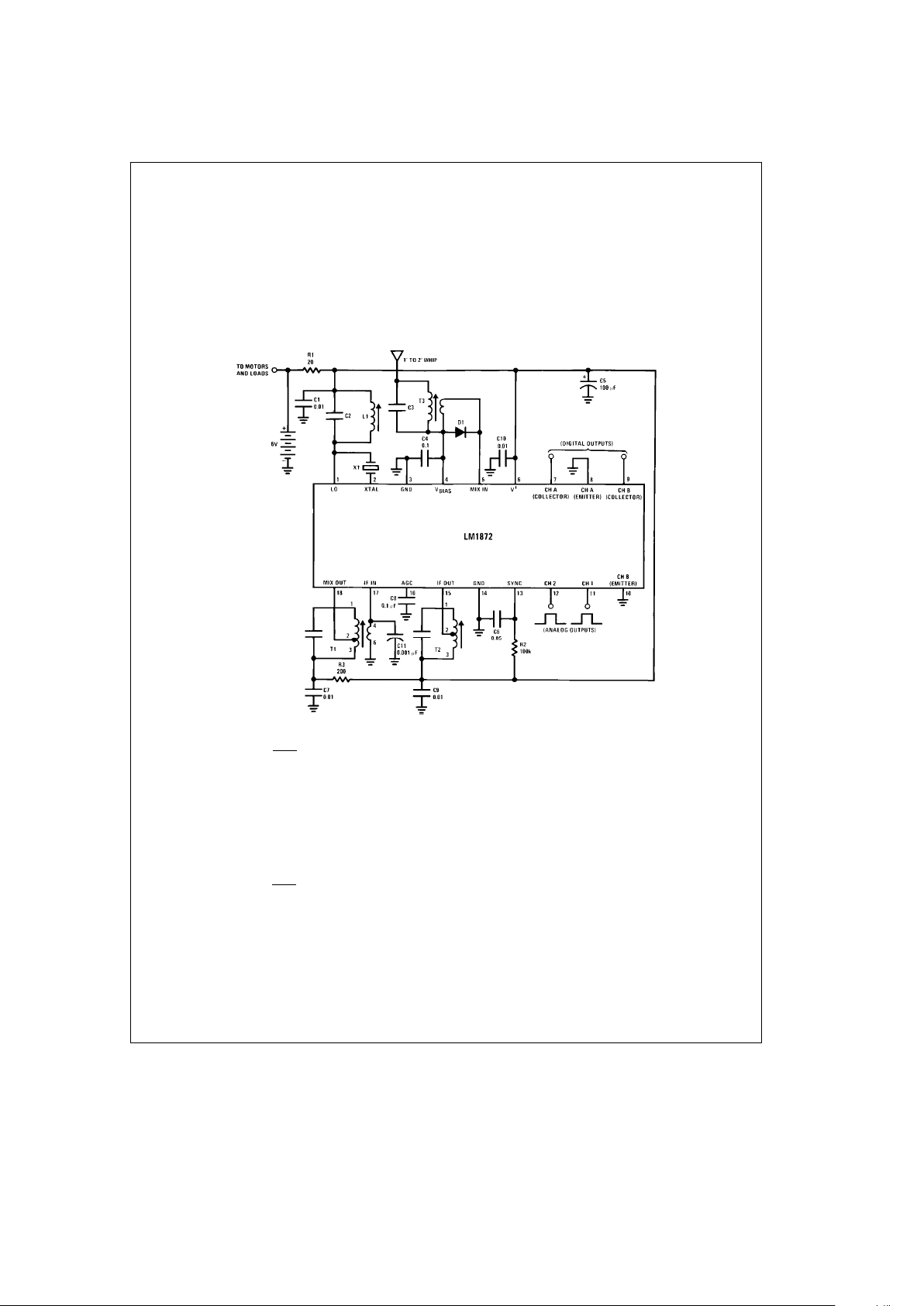
TL/H/7912– 11
R1 Ð Motor decoupling
R2 Ð Sync timer; R2
e
t’
SYNC
0.7 C6
,R2
s
470k
R3 Ð Mixer decoupling
C1 Ð LO bypass; optional
C2 Ð LO tank; C2
e
43 pF@27 MHz
e
24 pF@49 MHz
C3 Ð Ant. input tank; C3
e
39 pF@27 MHz
e
24 pF@49 MHz
C4ÐV
BIAS
bypass
C5 Ð Motor decoupling
C6 Ð Sync timer; C6
e
t’
SYNC
0.7 R2
,C6
s
0.5 mF
C7 Ð Mixer decouple; 0.01 mF
sC7s
0.1 mF
C8 Ð AGC
C9 Ð IF bypass; optional
C10 Ð V
a
bypass; 0.01 mFsC10s0.1 mF
C11 Ð LO bypass
L1 Ð LO coil
Toko* 10k type (KXNA-4434 DZ) 9T; 0.8 m H
@
27 MHz
Toko* 10k type (KEN-4028 DZ) 6T; 0.4 m H
@
49 MHz
L1 could be made a fixed coil, if desired.
T1 Ð 455 kHz mixer transformer
Toko* 10 EZC type (RMC-202313 NO), Qu
e
110
Pin 1– 2, 131T; pin 2 –3, 33T
Pin 1– 3, 164T; pin 4 –6, 5T
T2 Ð 455 kHz IF transformer
Toko* 10 EZC type (RMC-402503 NO), Qu
e
110
Pin 1– 2, 98T; pin 2 –3, 66T
Pin 1– 3, 164T; pin 4 –6, 8T
T3 Ð Ant. input transformer
Toko* 10k type (KXNA-4434 DZ), 3T sec. & 9T pri. of 0.8 mH
@
27 MHz
Toko* 10k type (KEN-4028 DZ), 1(/2T sec. & 6T pri. of 0.4 mH
@
49 MHz
X1 Ð 3rd overtone parallel-mode crystal
D1 Ð Electrostatic discharge (ESD) protection *Toko America
1250 Feehanville Drive
Mount Prospect, IL 60056
(312) 297-0070
FIGURE 5. Typical Application Circuit for 27 MHz or 49 MHz
7
Page 8

Circuit Description (Continued)
and T3. This tank effectively keeps strong out-of-band signals such as FM and TV broadcast from cross-modulating
with the desired signal. When operating at 49 MHz or
72 MHz, CB interference is also effectively minimized. Image rejection is relatively low, however, being only 7 dB
@
49 MHz, but this does not present a problem due to the
usual absence of strong interfering signals 910 kHz below
the desired signal.
The antenna signal is stepped down and DC coupled to the
mixer which consists of the emitter-coupled pair Q1 and Q2.
Emitter-follower, Q1, feeds the common-base device, Q2,
while effectively buffering the antenna from the LO energy
delivered by Q4. Mixer transconductance is 4 mmhos at low
frequency (1 MHz) falling to 3.3 mmhos at the upper end
(72 MHz).
The local oscillator utilizes an emitter coupled pair, Q3 and
Q4, for accurate control of mixer drive, I
1
. Quiescently, Q3
and Q4 share I
1
set by 0.69V/R5, but healthy voltage
swings at pin 2 due to oscillation of Q3 implement thorough
switching of the differential pair. As a result, the full 1.8 mA
of drive ‘‘tailgates’’ (switches) the mixer emitter coupled
pair, Q1 and Q2. This current is well regulated from supply
voltage changes by the V
BIAS
circuitry. The TC of V
BIAS
is
positive by design in order to impress a positive TC on I
1
so
as to compensate for the temperature dependence of bipolar transconductance in the mixer. Inasmuch as Q4 operates as an emitter-gated, common-base-connected device,
excellent isolation between local oscillator and mixer is obtained. As long as pin 4 is properly bypassed, Q5 presents a
low impedance to the base of Q4, resulting in low oscillator
noise. The oscillator easily operates up to 72 MHz with overtone crystals operating parallel mode.
The mixer signal is stepped down from the high Q mixer
tank, T1, and DC coupled to the IF via a secondary winding.
The IF stage consists of Q7, Q8 and Q10 and delivers a
transconductance of 4 mmhos
@
455 kHz. The quiescent
current, I
2
, is set at 120 mAbyV
BIAS
and a 6.2k resistor.
Again, the positive TC of V
BIAS
is used to compensate for
the temperature dependence of transconductance. The impedance at the IF output, pin 15, is very high (
t
800k) permitting the IF transformer, T2, to operate at near unloaded
Q (110). The overall 3 dB bandwidth of the receiver section
is 3.2 kHz (see characteristic curves); this is narrow enough
to permit adjacent channel operation without interference
yet wide enough to pass the 500 ms modulation pulses (t
M
in
Figure 2
).
The IF signal is DC coupled to the digital detector which
consists of a high gain precision comparator, a 30 ms integrator, and a supply-referred 25 mV voltage reference.
Whenever the peak IF signal exceeds 25 mV, the comparator drives Q11 to reset the digital envelope detector capacitor, C12. Since it takes 30 ms for the 1 mA current source to
ramp C12 to the 3V (V
a
/2) necessary to fire the Schmitt
trigger, the presence of 455 kHz carrier (period
e
2.2 ms)
greater than 25 mVp will prevent C12 from ever reaching
this threshold. When the carrier drops out, the Schmitt trigger will respond 30 ms later. This delay (like that associated
with the burst response of the 455 kHz IF tanks) is constant
over the time interval of interest. Thus, it is of no consequence to timing accuracy because the LM1872 responds
only to negative edges in the decoder.
AGC is provided only to the IF; the mixer having sufficient
overload recovery for the magnitude of signals available
from a properly operating (i.e. good carrier ON/OFF ratio)
10,000 mV/m transmitter. The AGC differential amplifier
regulates the peak carrier level to 100 mV by comparing it to
an internal 100 mV supply-referred voltage reference. The
resultant error signal is amplified and drives Q9 via rectifier
diode, D1, to shunt current away from Q10. C8 provides
compensation for the AGC loop which spans a 70 dB range.
The 100 mV AGC reference is accurately ratioed to the
25 mV detector reference to permit a controlled amount of
brief carrier loss before dropping below detector threshold.
Once into AGC, typically 60% amplitude modulation of the
PWM carrier is possible before the detector will recognize
the interference (see characteristic curves). This kind of
noise immunity is invaluable when the troublesome effects
of other physically close toys or walkie-talkies on the same
or adjacent frequencies are encountered.
DECODER SECTION
The purpose of the decoder is to extract the time information from the carrier for the analog channels and the pulse
count information for the digital channels. The core of the
decoder is a three-stage binary counter chain comprising
flip-flops A, B, and C. The demodulated output from the detector Schmitt-trigger drives both the counter chain and the
sync timer (Q12, R2, C6, and another Schmitt trigger). When
the RF carrier drops out for the first modulation pulse, t
M
,
the falling edge advances the counter (see
Figure 2
). Dur-
ing the t
M
interval the sync timer capacitor is held low by
Q12. When the carrier comes up again for the variable
channel interval, t
CH
, C6 begins to ramp towards threshold
(V
a
/2) but is unable to reach it in the short time that is
available. At the end of the t
CH
period the carrier drops out
again, the counter advances one more, and the sequence is
repeated for the second analog channel. To decode the two
analog channels, 3-input NAND gates G1 and G2 examine
the counter chain binary output so as to identify the time
slots that represent those channels. Decoded in this manner, the output pulse width equals the sum of t
M
, a fixed
pulse, and t
CH
, a variable width pulse. A Darlington output
driver interfaces this repetitive pulse to standard hobby servos.
Following the transmission of the second analog channel, a
variable quantity from one to four, of fixed width pulses
(500 ms) are transmitted that contain the digital channel information. Up until the end of the pulse group frame period,
t
F
, the decoder responds as if these fixed pulses were analog channels but delivers no outputs. At the conclusion of
the frame the sync pulse, t
SYNC
, is sent. Since t
SYNC
is
always made longer than the sync timer period (t’
SYNC
e
3.5 ms), the sync timer will output a sync signal to the first of
two cascaded 10 ms one-shots. The first one-shot enables
AND gates G3
x
G6 to read the A and B flip-flops of the
counter into a pair of RS latches. The state of flip-flop A, for
example, is then stored and buffered to drive 100 mA sink or
source at the channel A digital output. An identical parallel
path allows the state of flip-flop B to appear at the channel
B power output. Upon conclusion of the 10 ms read pulse,
another 10 ms one-shot is triggered that resets the counter
to be ready for the next frame.
8
Page 9
Application Hints
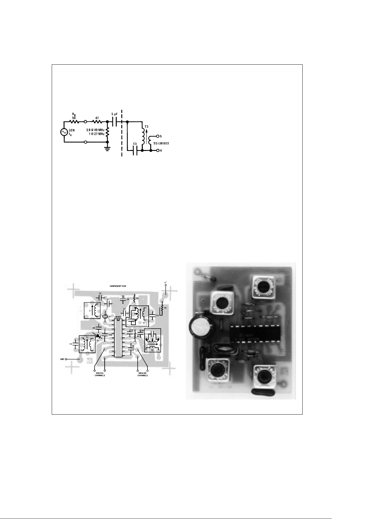
A typical application circuit for either 27 MHz or 49 MHz is
shown in
Figure 5
. Using the recommended antenna input
networks and driving the circuit through the antenna simulation network of
Figure 6
, a solid decoded output occurs for
10 mV and 12 mV input signals at 27 MHz and 49 MHz
respectively.
TL/H/7912– 12
FIGURE 6. Antenna Simulation Network
This sensitivity has been determined empirically to be optimum for toy vehicle applications. Less gain will reduce
range unacceptably and more gain will increase susceptibility to noise. However, should the application require greater
range (
l
50m for a land vehicle, for example), either the
antenna could be lengthened beyond 2
Ê
and/or receiver
sensitivity could be improved. There are a number of ways
to alter the sensitivity of the receiver. Decreasing the turns
ratio of input transformer, T3, for example, will couple more
signal into the mixer at the expense of lower tank Q due to
mixer loading. Moving the primary tap on mixer transformer,
T1, further from the supply side and/or decreasing the primary to secondary turns ratio will also increase gain. For
example, just changing T1 from a 32:1 primary to secondary
ratio to a 5:1 turns ratio (Toko
Ý
RMC202202) will double
49 MHz sensitivity (6 mVvs12mV). Mixer tank Q will be
affected but overall 3 dB BW will remain largely unchanged.
The primary tap on the IF transformer, T2, can also be adjusted (further from the supply side) for higher gain, but it is
possible to cause the AGC loop to oscillate with this method.
Narrow overall bandwidth is important for good receiver operation. The 3.2 kHz 3 dB bandwidth of the circuit in
Figure
5
is just wide enough to pass 500 ms carrier dropout pulses,
t
M
, yet narrow enough to hold down electrical noise and
reject potentially interfering adjacent channels. In the
49 MHz band, the five frequencies available are only 15 kHz
apart. Should only two frequencies be used simultaneously,
these channels could be chosen 60 kHz apart. Should three
frequencies be used, the spacing could be no more than
30 kHz. At four or five frequencies, 15 kHz spacings must be
dealt with, making narrow bandwidth highly desirable. Even
at 27 MHz, where allocated frequencies are 50 kHz apart,
the proliferation of CB stations only 10 kHz away represents
a formidable source of interference. The response of the
circuit of
Figure 5
is 34 dB and 56 dB down at 15 kHz and
50 kHz away, respectively (see characteristic curves).
The sync timer should have a timeout, t’
SYNC
, set longer
than the longest channel pulse transmitted, but shorter than
the shortest sync pulse, t
SYNC
, transmitted. Using the com-
ponent values in
Figure 5
,t’
SYNC
,e3.5 ms, which works
well with a transmitted sync pulse, t
SYNC
t
5 ms.
Numerous bypass capacitors appear in the circuit of
Figure
5
, not all of which may be necessary for good stability and
performance. A low cost approach may eliminate one or
more of the capacitors C1, C9, C10, and C11. The cleaner
and tighter the PCB layout used, the more likely is the case
that bypass capacitors can be eliminated. In the case of
marginal board stability, increasing the size of capacitors
C7, C9, and C10 to 0.1 mF may prove helpful. If the PCB
layout and parts loading diagram shown in
Figure 7
is used,
the circuit will be quite stable up to 72 MHz.
TL/H/7912– 13
TL/H/7912– 14
FIGURE 7. PCB Layout, Stuffing Diagram and Complete
RX Module for Typical Application Circuit of
Figure 5
9
Page 10

Application Hints (Continued)
The digital channel output devices have significant drive capability; they can typically sink 100 mA and possess a 7X
saturation resistance. Through their emitters they can
source 100 mA up to 1V above ground for driving grounded
NPNs and SCRs. Unfortunately, this kind of drive capability
can cause thermally induced chip destruction unless total
power dissipation is limited to less than 1000 mW. It is good
practice and highly recommended to allow the digital output
devices to fully saturate at all times (sinking or sourcing) and
to limit the current at saturation to no more than 100 mA.
For extra drive the two digital outputs can always be
summed by connecting pin 7 to pin 9.
The IF frequency is not constrained to be 455 kHz. Operation is limited on the high end to about 1 MHz due to the
frequency response limitations of the active detector. The
low end is limited to about 50 kHz due to the envelope
detector integration time
(Figure 4)
.
RECEIVER ALIGNMENT
The receiver alignment procedure is relatively straightforward because of an absence of interaction between the adjustments. First, the oscillator is tuned by adjusting L1 while
monitoring the LO signal at pin 2 with a low capacity
(j10 pF) probe. During tuning the amplitude will rise, peak,
and then abruptly quit. Adjust the coil away from the quitting
point and just below the amplitude peak.
In order to properly tune T1, T2, and T3, the RF signal must
be provided through the receiver antenna by the specific
transmitter which is to be used with that specific receiver.
This is because the crystals which are commonly used with
these systems may have tolerances as loose as
g
0.01%.
At 49 MHz the resultant
g
5 kHz deviation could easily put
the incoming signal out of the 3.2 kHz receiver IF bandpass.
The signal should be coupled through the receiving antenna
to ensure proper loading of the T3 input tank.
Alignment is easier with a defeated AGC, which is accomplished by merely grounding pin 16. The amplitude of the
455 kHz signal at pin 15 is used to guide alignment. Care
should be exercised that the signal swing not exceed roughly 400 mVp or diode, D2, in
Figure 4
will threshold and
clamp the waveform. Also note that a standard 10 pF probe
at pin 15 will shift the IF tank frequency an undesirable
2 kHz. Unless a lower capacity probe is available, it is recommended that the signal be monitored at the unused secondary of T2. Although the signal amplitude would be down
by a factor of 8.25 relative to pin 15, up to 50 pF probe
capacitance could be tolerated with negligible frequency
shift.
The incoming signal is obtained by removing the antenna
from the transmitter and then locating the transmitter at a
sufficient distance from the receiver to give a convenient
signal level (
s
400 mVp) at pin 15. T3, T1, and T2 are then
tuned for maximum signal.
Applications
OPERATION AT 72 MHz
The licensed 72 MHz band is popular among hobby enthusiasts for controlling aircraft. The higher transmitted power
levels that the FCC allows yield much greater operating
range and the frequency band is uncluttered relative to
27 MHz. Elevated frequencies such as 72 MHz are no problem with the LM1872. The part is stable and will provide
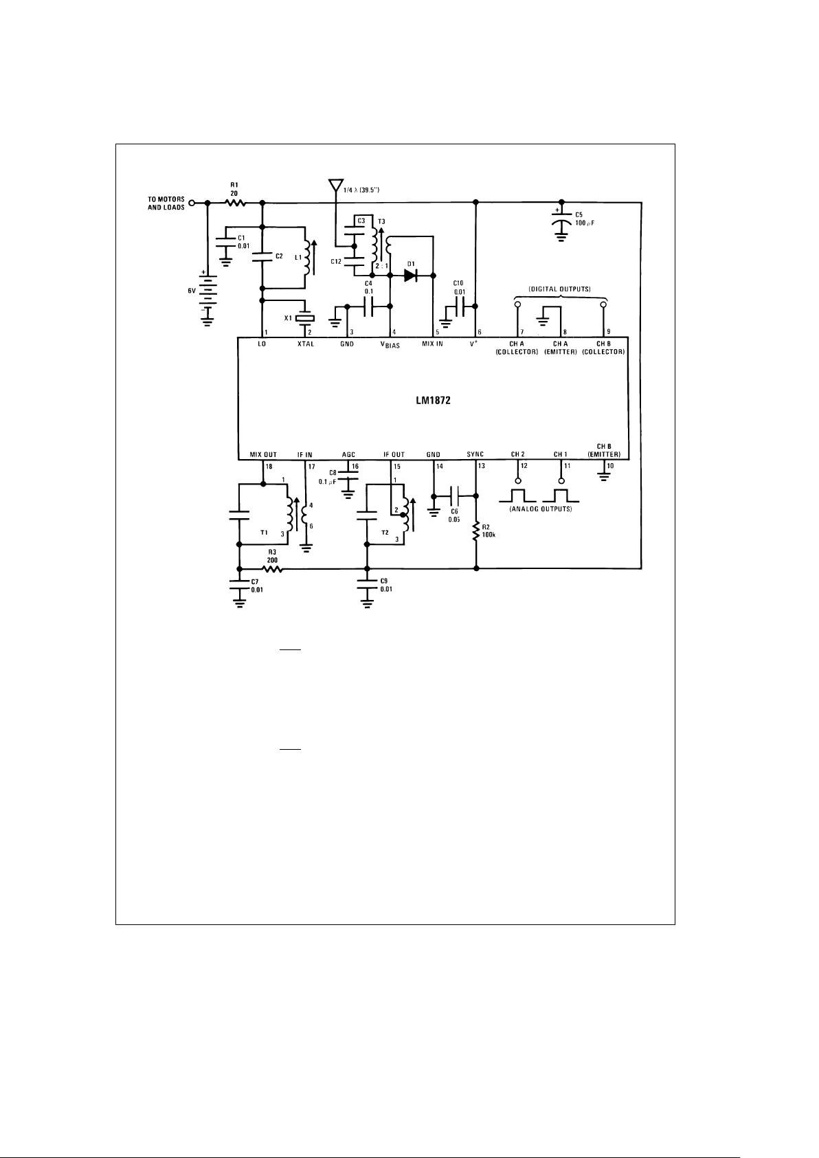
good sensitivity and selectivity at that frequency. The application circuit in
Figure 8
will provide a set of solid decoded
outputs for
k
2 mV of signal at the antenna input, which is
designed to match the 100X resistive impedance of the (/4
wavelength antenna. IF bandwidth is a respectable 3.2 kHz.
For good immunity to overload from a very closely (antennas touching) operating high power transmitter, the transmitter design should emphasize a high carrier ON/OFF ratio. Using the LM1871 as a low power exciter to drive one or
more external class C power amplifier stages will result in a
simple, acceptable, low cost transmitter at 72 MHz.
Inasmuch as many hobby applications require more analog
channels than the LM1872 normally provides, particular attention should be paid to
Figures 10 and 12
which describe
how to expand analog channel capacity up to 4 and 6 channels, respectively.
OPERATION WITH AN IR CARRIER
An infra-red (or visible) light data link is a useful alternative
to its RF counterpart. Should the application demand that
the radiation not leave the room, or that it be directional, or
not involve FCC certification then a light carrier should be
given consideration. The principal drawbacks to this approach include short range (
s
20 ft.) and high transmitter
power consumption. There is little that can be done to dramatically improve range, but short burst-type operation of
the transmitter will still permit battery operation.
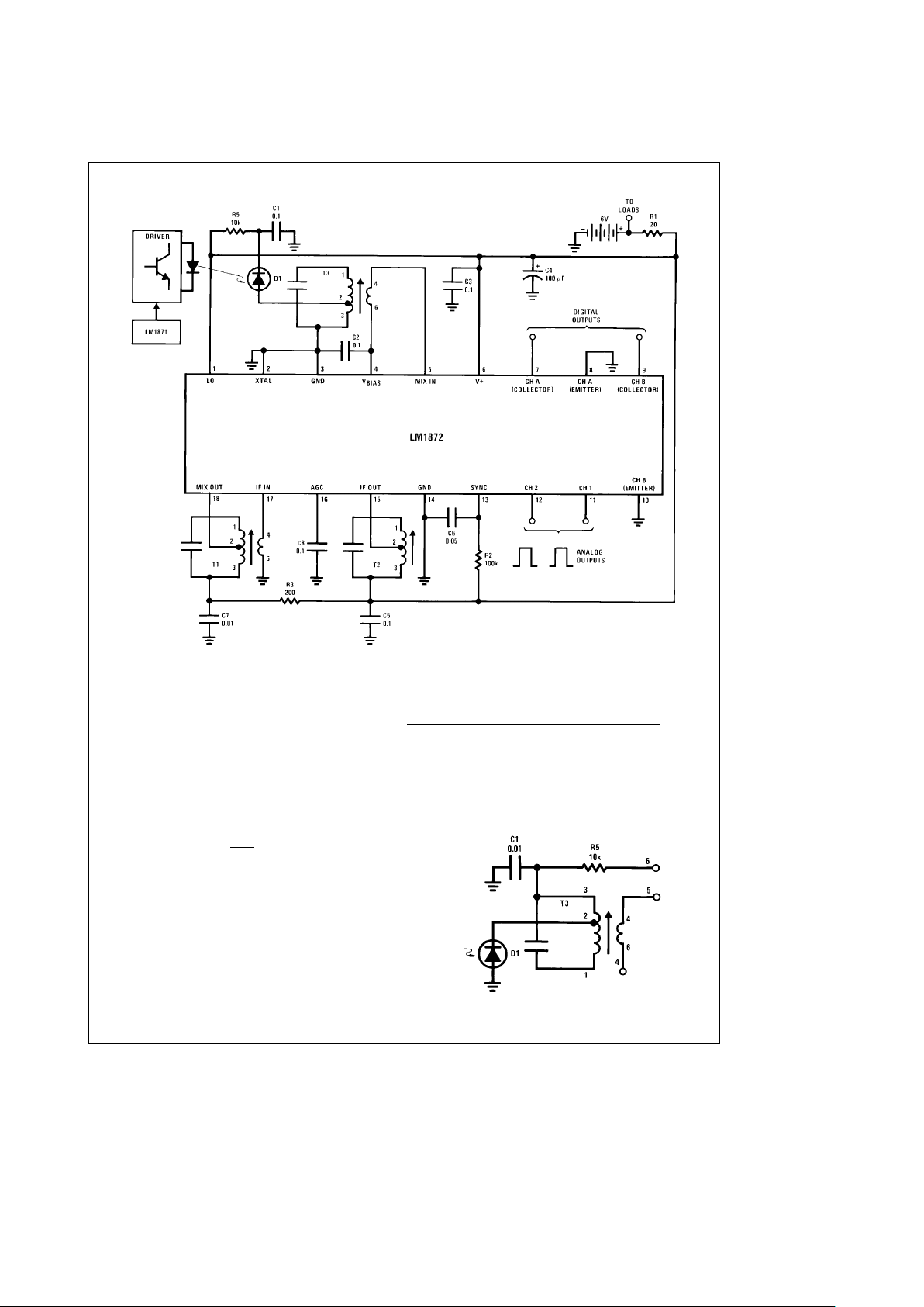
The information link
(Figure 9a)
consists of a light carrier
amplitude modulated by a 455 kHz subcarrier. The subcarrier in turn is modulated by the normal Pulse Width/Pulse
Count Scheme produced by the LM1871 encoder. A husky,
focused LED is used as the transmitter running Class A
100% modulated with an average current drain of 50 mA to
500 mA depending upon range requirements. The detector
consists of a large area silicon PN or PIN photodiode for
good sensitivity. The LM1872 will directly interface to such a
diode and give very good performance. Only a few nanoamps of photo current from D1 are required to threshold
the detector. Ambient light rejection is excellect due to the
very narrow bandwidth (j3 kHz) that results from the use
of three high Q 455 kHz transformers, T1, T2, and T3. Note
that the LO has been defeated and the mixer runs as a
conventional 455 kHz amplifier. Otherwise, circuit operation
is the same as if an RF carrier were being received.
10
Page 11
Applications (Continued)
TL/H/7912– 15
R1 Ð Motor decoupling
R2 Ð Sync timer; R2
e
t’
SYNC
0.7 C6
,R2
s
470k
R3 Ð Mixer decoupling
C1 Ð LO bypass; optional
C2 Ð LO tank; C2
e
22 pF@72 MHz
C3 Ð Ant. input tank; C3
e
24 pF@72 MHz
C4 Ð V
BIAS
bypass
C5 Ð Motor decoupling
C6 Ð Sync timer; C6
e
t’
SYNC
0.7 R2
,C6
s
0.5 mF
C7 Ð Mixer decouple; 0.01 mF
sC7s
0.1 mF
C8 Ð AGC
C9 Ð IF bypass; optional
C10 Ð V
a
bypass; 0.01 mFsC10s0.1 mF
C12 Ð Ant. input tank; C12
e
160 pF@72 MHz
L1 Ð LO Coil
Toko 10k type (KENC) 4T; 0.2 mH
@
72 MHz
L1 could be made a fixed coil, if desired
T1 Ð 455 kHz mixer transformer
Toko 10 EZC type (RMC-502182), Qu
e
110
Pin 1– 2, 82T; pin 2 –3, 82T
Pin 1– 3, 164T; pin 4 –6, 30T
T2 Ð 455 kHz IF transformer
Toko 10 EZC type (RMC-502503), Qu
e
110
Pin 1– 2, 82T; pin 2 –3, 82T
Pin 1– 3, 164T; pin 4 –6, 8T
T3 Ð Ant. input transformer
Toko 10k type (KENC), 4T sec &
2T pri. of 0.2 mH
@
72 MHz
X1 Ð 5th overtone crystal, parallel-mode, 72 MHz
D1 Ð Electrostatic discharge (ESD) protection
FIGURE 8. 72 MHz Receiver Circuit
In a practical remote data link, the transmitter could be battery operated and set up to transmit for brief intervals only in
order to save power. The brief transmission could be used
to set or reset the digital output latches in the LM1872 and/
or command new motor positions via the analog channels.
After transmission, the commands would be stored electri-
cally in the case of the digital channels and mechanically in
the case of the analog channels.
As a final note, if the case of D1 is connected to the anode
rather than the cathode, the circuit of
Figure 9b
should be
used at the input to maintain electromagnetic shielding.
11
Page 12
Applications (Continued)
TL/H/7912– 16
Bottom View
FIGURE 9a. IR Type Data Link
R1 Ð Load decoupling
R2 Ð Sync timer; R2
e
t
0.7 C6
,R2
s
470k
R3 Ð Preamp decoupling
R5 Ð Photodiode decoupling
C1 Ð Photodiode decoupling
C2ÐV
BIAS
bypass
C3ÐV
a
bypass
C4 Ð Load decoupling
C5 Ð IF bypass; optional
C6 Ð Sync timer; C6
e
t
SYNC
0.7 R2
,C6
s
0.5 mF
C7 Ð Preamp decoupling
C8 Ð AGC
T1 Ð 455 kHz preamp transformer
Toko 10 EZC type (RMC-502182), Qu
e
110
Pin 1– 2, 82T; pin 2 –3, 82T
Pin 1– 3, 164T; pin 4-6, 30T
T2 Ð 455 kHz IF transformer
Toko 10 EZC type (RMC-402503), Qu
e
110
Pin 1– 2, 98T; pin 2 –3, 66T
Pin 1– 3, 164T; pin 4 –6, 8T
T3 Ð 455 kHz input transformer
Toko 10 EZC type (RMC-202313), Qu
e
110
Pin 1– 2, 131T; pin 2 –3, 33T
Pin 1– 3, 164T; pin 4 –6, 5T
D1 Ð PN or PIN Silicon Photodiode
Photodiode, D1 Active Area (cm2)
Vactec VTS 5088 0.18
Vactec VTS 6089 0.52
UDT PIN 6D or 6 DP 0.20
UDT PIN 220 DP 2.0
Siemens BPY 12 0.20
TL/H/7912– 17
FIGURE 9b. Input Stage Where the Case of D1 is
Connected to the Anode
12
Page 13
Applications (Continued)
EXPANSION TO FOUR ANALOG CHANNELS
For those applications that require more than the two analog channels that are normally provided, the LM1872 can
easily be expanded to 4 channels with appropriate external
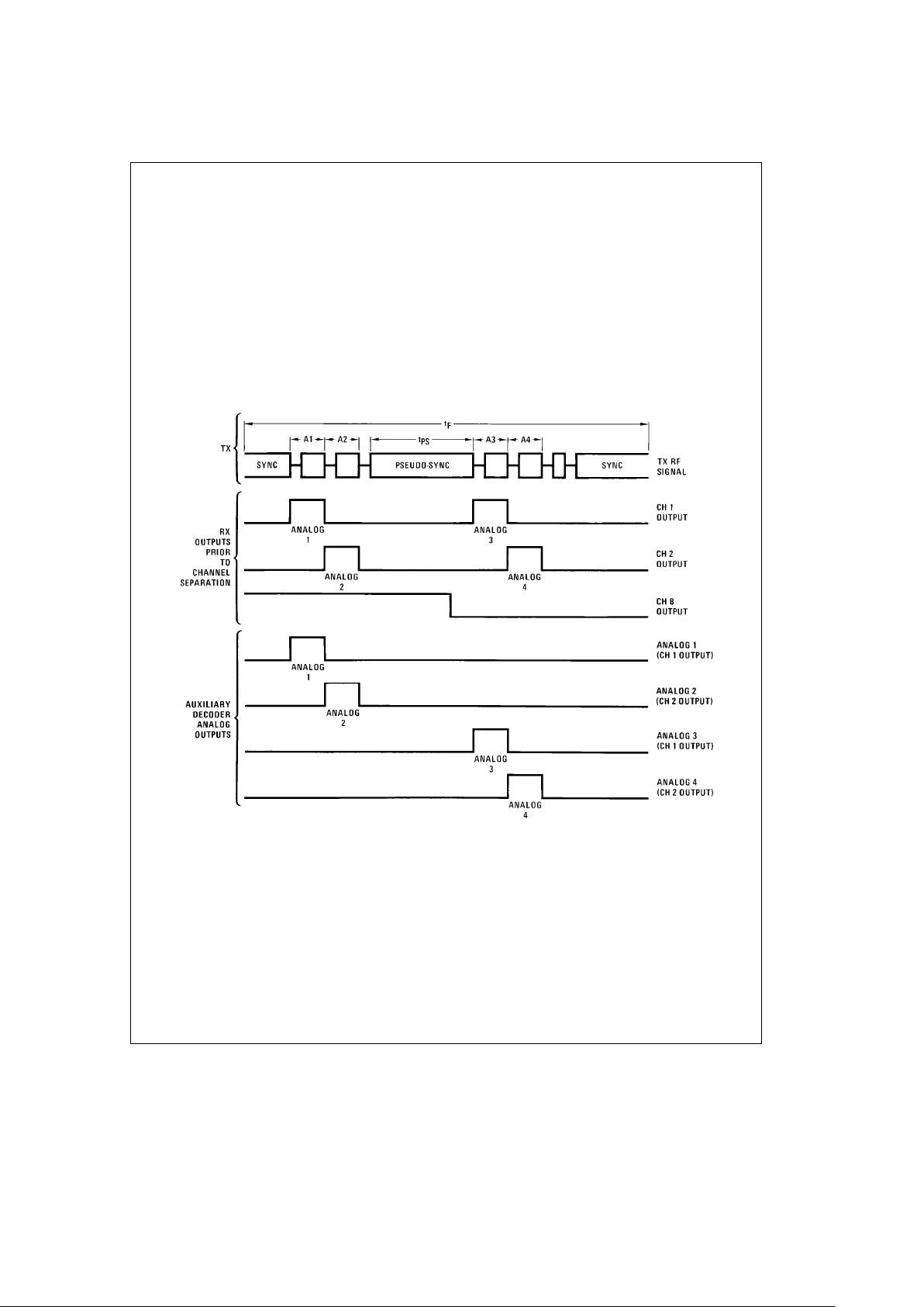
circuitry. This is accomplished by creating a pseudo-sync
pulse (t
ps
) among a six channel transmitted frame from the
LM1871
(Figure 10)
. The pseudo-sync pulse deceives the
decoder in the LM1872 causing premature recognition of
end-of-frame, effectively splitting a single frame into two.
The idea is to transmit analog channels 1 and 2 in the first
half of the normal frame period and analog channels 3 and
4 in the second half. External logic will then steer the four
channels from the LM1872’s only two analog output pins
into four new analog outputs. Steering is accomplished with
the help of one of the digital channels. Inasmuch as the
digital channels respond only to the
number
of pulses re-
ceived between any two sync (or pseudo-sync!) pulses, the
channels are capable of toggling in step with the alternating
transmission of two and three channel pulse mini-groups
occurring within each half frame.
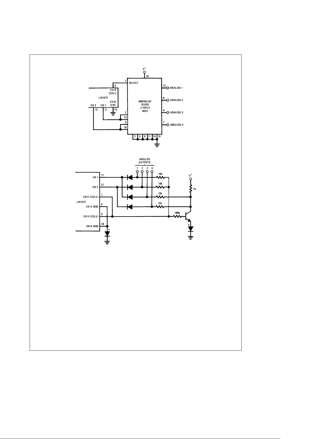
Figure 10a
reveals that
both digital channels A and B are high during the dual pulse
half frame and low during its triple pulse counterpart.
Figure
10b
shows just how simple the external circuitry can be.
Digital channel B drives the channel select pin of a quad 2input MUX that routes the LM1872 channels 1 and 2 outputs
to the four new outputs labeled analog 1 through 4.
Although not the model of simplicity of
Figure 10b, Figure
10c
is a lower cost alternative that works just as well. The
diodes with the asterisk prevent a ground step from occurring that could false trip an excessively edge sensitive servo
and can be eliminated in many cases.
TL/H/7912– 18
a) Transmitter, Receiver, and Auxiliary Decoder Timing Diagram
FIGURE 10. Deriving Four Analog Channels Through the Use of an Auxiliary Decoder
13
Page 14
Applications (Continued)
TL/H/7912– 19
b) Simple Decoding of Four Analog Channels with CMOS
*See Text
TL/H/7912– 20
c) Low-Cost Decoding of Four Analog Channels with DTL
FIGURE 10. Deriving Four Analog Channels Through the Use of an Auxiliary Decoder (Continued)
FOUR SINGLE CHANNEL RECEIVERS
DRIVEN FROM A SINGLE TRANSMITTER
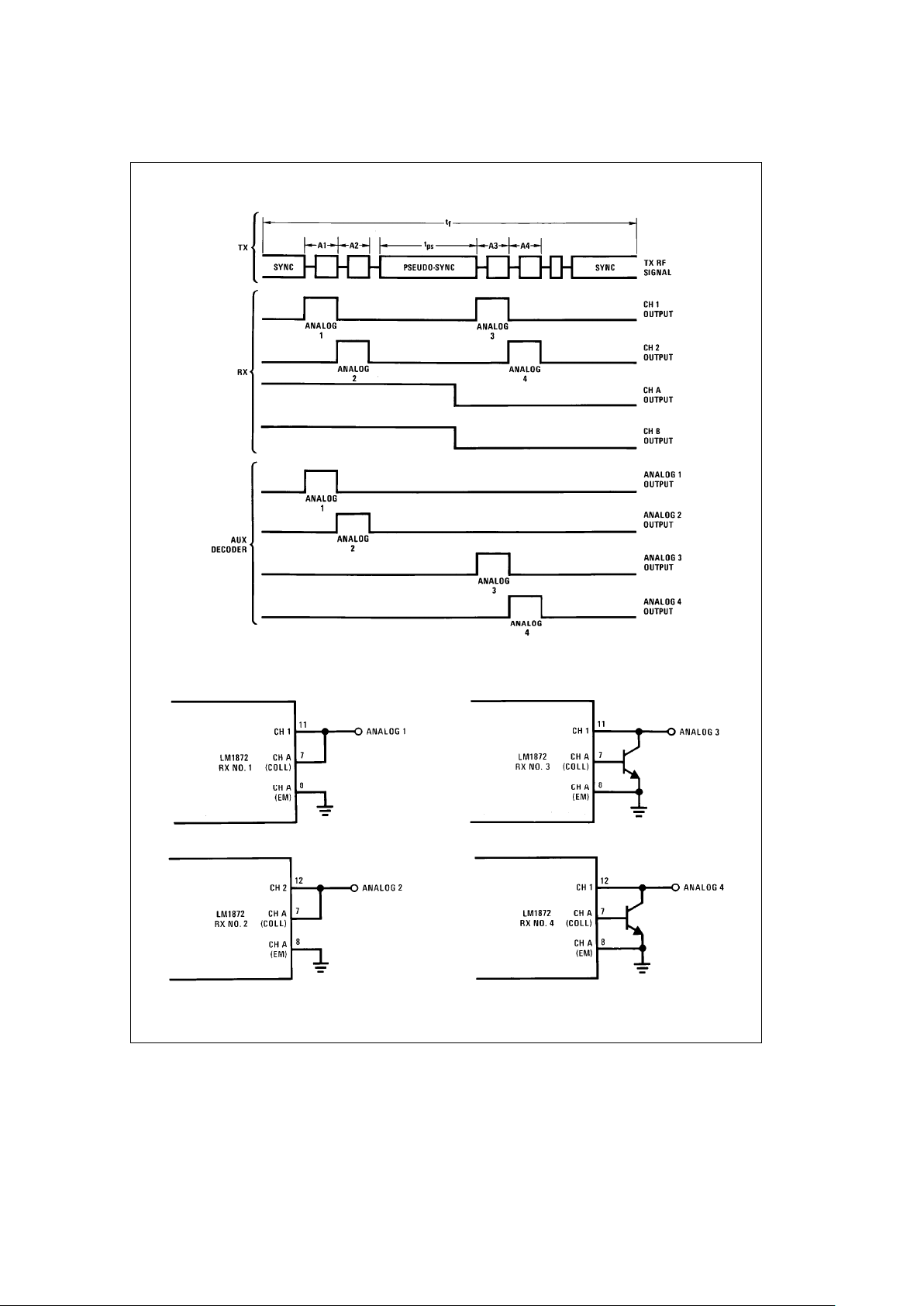
When it is desired to control more than two vehicles or remote stations with the analog information from a single
transmitter, the LM1872 can be put to the task. By utilizing
the frame splitting technique previously described in
Figure
10
, up to four independent single analog channel receivers
can be made to operate from a single transmitter
(Figure
11)
. Toggling digital channel A, either directly or through an
inversion, is used to suppress a given receiver’s analog output when the undesired analog channels are transmitted. In
this manner, only the desired analog channel is outputted at
each receiver. The amount of external circuitry required to
do this is minimal; two receivers require a single transistor
apiece while the other two receivers need no extra parts at
all.
14
Page 15
Applications (Continued)
TL/H/7912– 21
a) Transmitter, Receiver, and Separated Channels Timing Diagram
TL/H/7912– 22
b) Simple Channel Separation with Two External Transistors
FIGURE 11. Obtaining Four Independent Single Analog Channel Receivers from a Single Common Transmitter
15
Page 16
Applications (Continued)
EXPANSION TO SIX ANALOG CHANNELS
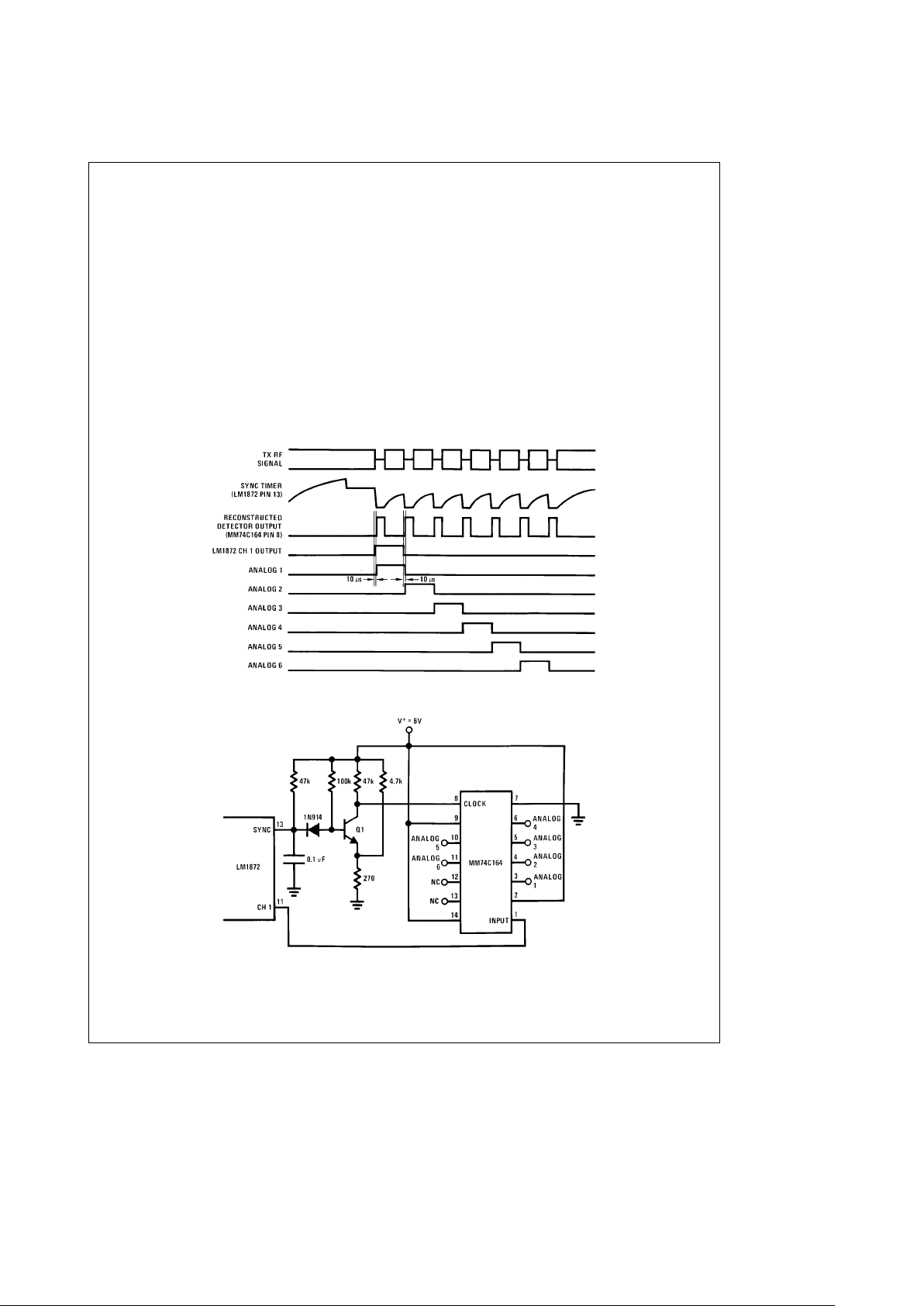
Still greater analog capacity can be obtained with an outboard auxiliary decoder. The LM1872, a simple comparator,
and an 8-bit parallel-out serial shift register comprise a six
analog channel receiver/decoder
(Figure 12)
. The one transistor comparator reconstructs the detector output of the
LM1872 from the sync timer waveform and feeds it to the
clock input of the shift register. The channel 1 output then
loads a ‘‘one’’ into the register and the clock shifts the
‘‘one’’ down the line of analog channel outputs in accordance with the time information from the detector output.
Note that the reconstructed detector waveform lags the
channel 1 output very slightly (j10 ms) due to the finite
slope of the sync capacitor discharge edge. This delay is
very important as it insures that channel 1 is high when the
clock strikes initially (thus loading a ‘‘1’’) and low for each
subsequent positive clock edge (thus preventing the loading
of extraneous ‘‘1’s’’).
CONVERTING AN ANALOG CHANNEL
TO A DIGITAL CHANNEL
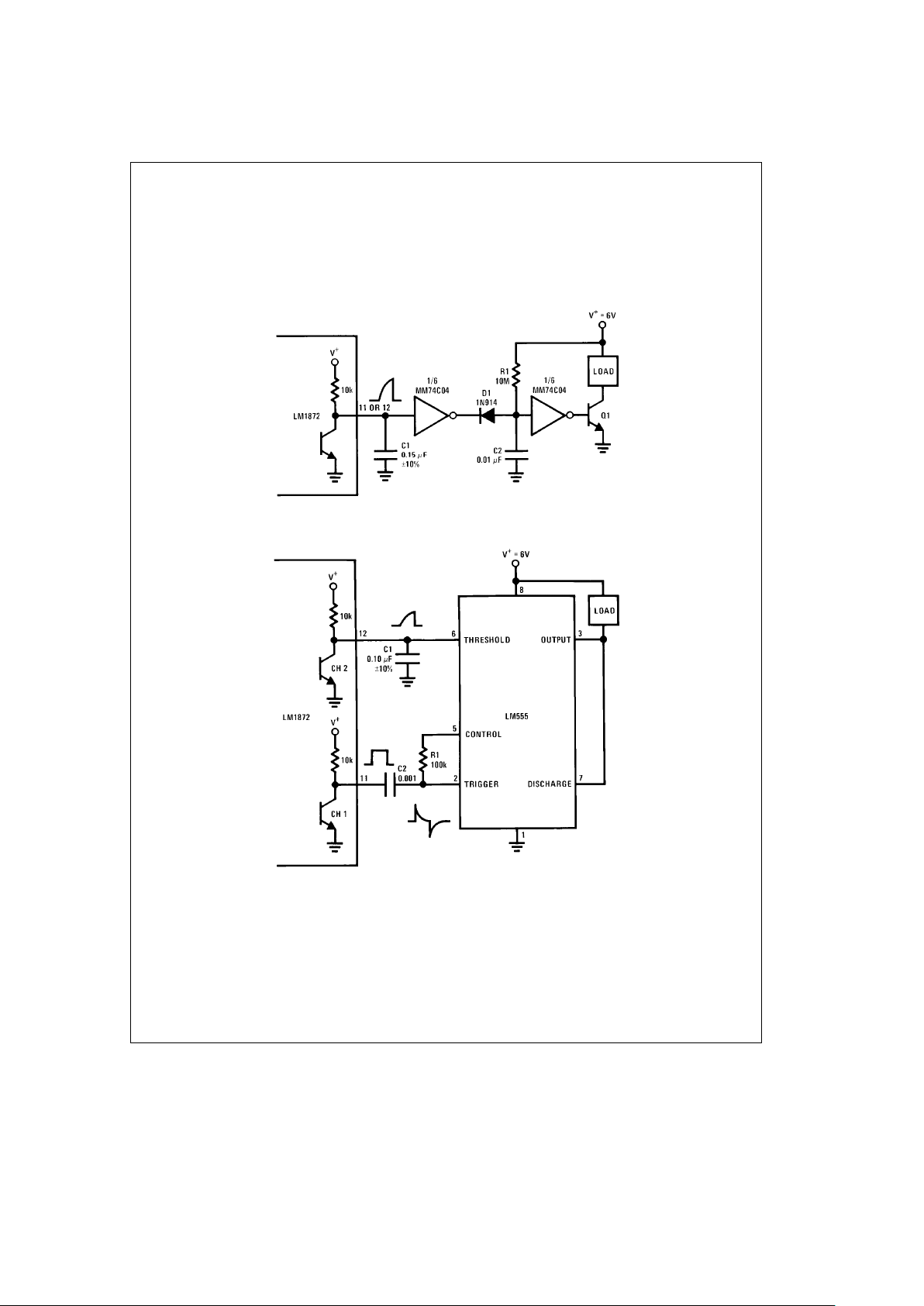
Either analog channel can be converted to a digital channel
with the aid of a low cost CMOS hex inverter
(Figure 13)
.
The internal 10k resistor and external capacitor, C1, set a
time constant (1 ms) that falls between a short (0.5 ms) and
a long (2 ms) transmitted pulse option. For pulses longer
than 1 ms, the first inverter will pull low momentarily once
each frame. Repetitive discharges of C2 prevent it from ever
reaching threshold (V
a
/2) because the R1 C2 time constant is set longer (70 ms) than the frame period. With the
inverter input below threshold, Q1 will energize the load. For
analog output pulses shorter than 1 ms, the first inverter will
back bias D1 allowing C2 to ramp past threshold and Q1 to
go off. For extra output drive, the remaining inverters in the
package can be paralleled to drive Q1. Alternatively, for light
loads Q1 can be eliminated altogether.
TL/H/7912– 23
a) Six Channel Timing Diagram
TL/H/7912– 24
b) Six Channel Auxiliary Decoder
FIGURE 12. Deriving Six Analog Channels
16
Page 17
Applications (Continued)
Where only one of the two available analog channels needs
conversion to a digital format, the LM555 approach offers
simplicity combined with up to 150 mA of output drive
(Fig-
ure 14)
. The trailing edge of CH 1’s output pulse is used to
reset the timer in preparation for comparing CH 2’s pulse
width to the time constant (1.1 ms) set by the internal 10k
resistor and C1. For CH 2 pulse widths greater than 1.1 ms
C1 ramps to threshold, setting an internal latch in the
LM555 and causing the load to be energized. Due to the
timing of the reset pulse, however, the LM555 output will go
high again for 1.1 ms during the next pulse comparison cycle thus producing an ON state duty cycle of about 95%.
For most commonly encountered loads such as motors, solenoids, lamps, and horns, this is of little consequence. The
OFF state duty cycle is 100%.
TL/H/7912– 25
FIGURE 13. Conversion of an Analog Channel
to a Digital (On/Off) Channel
TL/H/7912– 26
FIGURE 14. Simple Conversion of an Analog to a Digital Channel
17
Page 18
Applications (Continued)
BRIDGE DRIVING A MOTOR
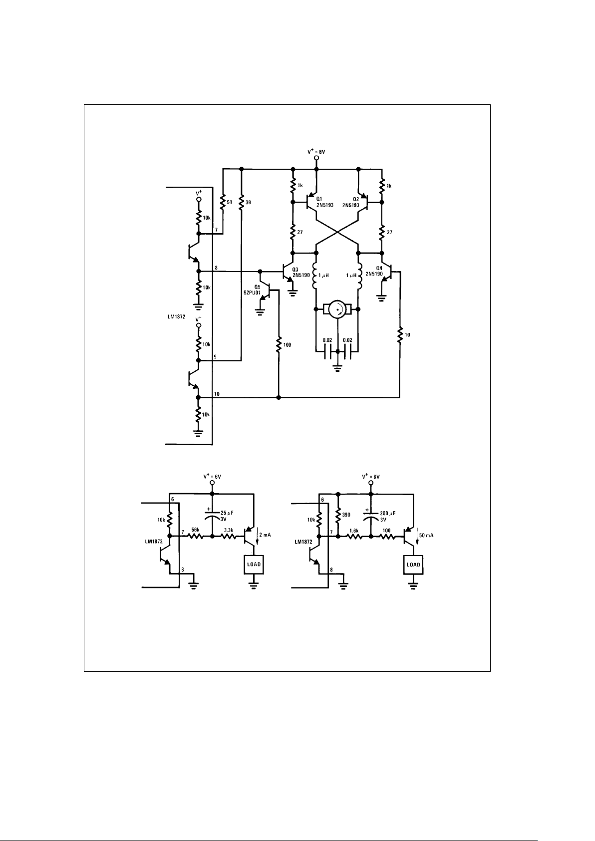
The two digital channels can be used to propel a car forward, off, and reverse without the need for a costly servo
(Figure 16)
. The 100 mA digital output capability is used to
drive a bridge of four transistors with Q5 added as a protection device. Should an erroneous command to power both
sides of the bridge occur (as may happen due to noise with
the car out of range) the large motor drive transistors would
fight one another resulting in the thermal destruction of one
or more of those devices. But Q5 will disable the left side of
the bridge whenever the right side is powered, preventing
the problem from ever occurring. The motor noise suppression network shown has proven to be especially effective in
reducing electrical noise and is therefore highly recommended.
NOISE INTEGRATION OF A DIGITAL CHANNEL
Commonly available inexpensive DC motors are a formidable source of electromagnetic interference. Radiation can
come from the power feed leads and/or directly from the
brushes. Usually proper lead dress and board orientation
coupled with a good filter network (
see Figure 16
) will eliminate any problems. In particularly stubborn cases of motor
interference, the digital channels may experience more objectionable interference than the analog channels. This is
generally not because the digital channels are more susceptible, but rather because the type of load they typically drive
(i.e. a horn) will make more of a nuisance of itself than a
typical analog load (i.e. a steering servo) when subjected to
interference.
Straightforward time integration of the digital channel outputs works very well with any type or degree of motor interference. The simple circuits of
Figure 17
integrate over a
period of about three frames (70 ms) and have approximately equal delay either going off or coming on.
TL/H/7912– 27
FIGURE 15. Interfacing Directly to Standard Hobby Servos
18
Page 19
Applications (Continued)
TL/H/7912– 28
FIGURE 16. Digital Bridge Motor Drive
TL/H/7912– 29
a) Low Current Load b) High Current Load
FIGURE 17. Integrating a Digital Channel Output to Achieve Noise Immunity
19
Page 20
LM1872 Radio Control Receiver/Decoder
Physical Dimensions inches (millimeters)
Molded Dual-In-Line Package (N)
Order Number LM1872N
NS Package Number N18A
LIFE SUPPORT POLICY
NATIONAL’S PRODUCTS ARE NOT AUTHORIZED FOR USE AS CRITICAL COMPONENTS IN LIFE SUPPORT
DEVICES OR SYSTEMS WITHOUT THE EXPRESS WRITTEN APPROVAL OF THE PRESIDENT OF NATIONAL
SEMICONDUCTOR CORPORATION. As used herein:
1. Life support devices or systems are devices or 2. A critical component is any component of a life
systems which, (a) are intended for surgical implant support device or system whose failure to perform can
into the body, or (b) support or sustain life, and whose be reasonably expected to cause the failure of the life
failure to perform, when properly used in accordance support device or system, or to affect its safety or
with instructions for use provided in the labeling, can effectiveness.
be reasonably expected to result in a significant injury
to the user.
National Semiconductor National Semiconductor National Semiconductor National Semiconductor
Corporation Europe Hong Kong Ltd. Japan Ltd.
1111 West Bardin Road Fax: (
a
49) 0-180-530 85 86 13th Floor, Straight Block, Tel: 81-043-299-2309
Arlington, TX 76017 Email: [email protected] Ocean Centre, 5 Canton Rd. Fax: 81-043-299-2408
Tel: 1(800) 272-9959 Deutsch Tel: (
a
49) 0-180-530 85 85 Tsimshatsui, Kowloon
Fax: 1(800) 737-7018 English Tel: (
a
49) 0-180-532 78 32 Hong Kong
Fran3ais Tel: (
a
49) 0-180-532 93 58 Tel: (852) 2737-1600
Italiano Tel: (
a
49) 0-180-534 16 80 Fax: (852) 2736-9960
National does not assume any responsibility for use of any circuitry described, no circuit patent licenses are implied and National reserves the right at any time without notice to change said circuitry and specifications.
 Loading...