

Page 1

LM146/LM346
Programmable Quad Operational Amplifiers
LM146/LM346 Programmable Quad Operational Amplifiers
May 1999
General Description
The LM146 series of quad op amps consists of four independent, high gain, internally compensated, low power, programmable amplifiers. Two external resistors (R
the user to program the gain bandwidth product, slew rate,
supply current, input bias current, input offset current and input noise. For example, the user can trade-off supply current
for bandwidth or optimize noise figure for a given source resistance. In a similar way, other amplifier characteristics can
be tailored to the application. Except for the two programming pins at the end of the package, the LM146 pin-out is
the same as the LM124 and LM148.
SET
) allow
Connection Diagram
Dual-In-Line Package
DS005654-1
Order Number LM146J, LM146J/883,
Top View
LM346M or LM346N
See NS Package Number
J16A, M16A or N16A
Features
=
(I
10 µA)
SET
n Programmable electrical characteristics
n Battery-powered operation
n Low supply current: 350 µA/amplifier
n Guaranteed gain bandwidth product: 0.8 MHz min
n Large DC voltage gain: 120 dB
n Low noise voltage: 28
n Wide power supply range:±1.5V to±22V
n Class AB output stage–no crossover distortion
n Ideal pin out for Biquad active filters
n Input bias currents are temperature compensated
PROGRAMMING EQUATIONS
SET
/10 µA)
SET
SET
/10 µA)
/10 µA)
Total Supply Current=1.4 mA (I
Gain Bandwidth Product=1 MHz (I
Slew Rate=0.4V/µs (I
Input Bias Current
=
I
Current into pin 8, pin 9 (see schematic-diagram)
SET
≅
50 nA (I
SET
/10 µA)
© 1999 National Semiconductor Corporation DS005654 www.national.com
Page 2

Schematic Diagram
DS005654-2
www.national.com 2
Page 3

Absolute Maximum Ratings (Notes 1, 5)
If Military/Aerospace specified devices are required, please contact the National Semiconductor Sales Office/
Distributors for availability and specifications.
LM146 LM346
Supply Voltage
Differential Input Voltage (Note 1)
CM Input Voltage (Note 1)
±
22V
±
30V
±
15V
±
18V
±
30V
±
15V
Power Dissipation (Note 2) 900 mW 500 mW
Output Short-Circuit Duration (Note 3) Continuous Continuous
Operating Temperature Range −55˚C to +125˚C 0˚C to +70˚C
Maximum Junction Temperature 150˚C 100˚C
Storage Temperature Range −65˚C to +150˚C −65˚C to +150˚C
Lead Temperature (Soldering, 10 seconds) 260˚C 260˚C
Thermal Resistance (θ
), (Note 2)
jA
Cavity DIP (J) Pd 900 mW 900 mW
Small Outline (M) θ
θ
jA
jA
100˚C/W 100˚C/W
115˚C/W
Molded DIP (N) Pd 500 mW
θ
jA
90˚C/W
Soldering Information
Dual-In-Line Package
Soldering (10 seconds) +260˚C +260˚C
Small Outline Package
Vapor Phase (60 seconds) +215˚C +215˚C
Infrared (15 seconds) +220˚C +220˚C
SeeAN-450 “Surface Mounting Methods and Their Effect on Product Reliability” for other methods of soldering surface mount devices.
ESD rating is to be determined.
DC Electrical Characteristics
=
±
(V
S
Input Offset Voltage V
Input Offset Current V
Input Bias Current V
Supply Current (4 Op Amps) T
Large Signal Voltage Gain R
Input CM Range T
CM Rejection Ratio R
Power Supply Rejection Ratio R
Output Voltage Swing R
Short-Circuit T
Gain Bandwidth Product T
Phase Margin T
Slew Rate T
Input Noise Voltage f=1 kHz, T
=
15V, I
10 µA), (Note 4)
SET
Parameter Conditions LM146 LM346 Units
Min Typ Max Min Typ Max
=
0V, R
CM
CM
CM
A
L
T
A
A
S
S
V
S
L
A
A
A
A
S
=
0V, T
A
=
0V, T
A
=
25˚C 1.4 2.0 1.4 2.5 mA
=
10 kΩ, ∆V
=
25˚C
=
25˚C
≤10 kΩ,T
≤10 kΩ,T
=
±
5to±15V
≥10 kΩ,T
=
25˚C 5 20 35 5 20 35 mA
=
25˚C 0.8 1.2 0.5 1.2 MHz
=
25˚C 60 60 Deg
=
25˚C 0.4 0.4 V/µs
=
A
=
≤50Ω,T
=
=
A
A
A
25˚C 0.5 5 0.5 6 mV
A
25˚C 2 20 2 100 nA
25˚C 50 100 50 250 nA
=
±
10V, 100 1000 50 1000 V/mV
OUT
±
13.5±14
=
25˚C 80 100 70 100 dB
=
25˚C, 80 100 74 100 dB
=
25˚C
±
±
12
14
±
13.5±14 V
±
±
12
14 V
25˚C 28 28
Channel Separation R
Input Resistance T
Input Capacitance T
Input Offset Voltage V
=
10 kΩ, ∆V
L
±
12V, T
A
=
25˚C 1.0 1.0 MΩ
A
=
25˚C 2.0 2.0 pF
A
=
0V, R
CM
=
0V to 120 120 dB
OUT
=
25˚C
≤50Ω 0.5 6 0.5 7.5 mV
S
www.national.com3
Page 4

DC Electrical Characteristics (Continued)
=
±
(V
S
Input Offset Current V
Input Bias Current V
Supply Current (4 Op Amps) 1.7 2.2 1.7 2.5 mA
Large Signal Voltage Gain R
Input CM Range
CM Rejection Ratio R
Power Supply Rejection Ratio R
Output Voltage Swing R
=
15V, I
10 µA), (Note 4)
SET
Parameter Conditions LM146 LM346 Units
Min Typ Max Min Typ Max
=
0V 2 25 2 100 nA
CM
=
0V 50 100 50 250 nA
CM
=
10 kΩ, ∆V
L
≤50Ω 70 100 70 100 dB
S
≤50Ω, 76 100 74 100 dB
S
=
±
V
5V to±15V
S
≥10 kΩ
L
=
±
10V 50 1000 25 1000 V/mV
OUT
±
13.5±14
±
12
±
13.5±14 V
±
14
±
±
12
14 V
DC Electrical Characteristic
=
±
(V
S
Input Offset Voltage V
Input Bias Current V
Supply Current (4 Op Amps) T
Gain Bandwidth Product T
=
15V, I
SET
10 µA)
Parameter Conditions LM146 LM346 Units
Min Typ Max Min Typ Max
=
≤50Ω, 0.5 5 0.5 7 mV
0V, R
CM
T
A
CM
A
A
S
=
25˚C
=
=
0V, T
25˚C 7.5 20 7.5 100 nA
A
=
25˚C 140 250 140 300 µA
=
25˚C 80 100 50 100 kHz
DC Electrical Characteristics
=
±
(V
1.5V, I
S
Parameter Conditions LM146 LM346 Units
Input Offset Voltage V
Input CM Range T
CM Rejection Ratio R
Output Voltage Swing R
Note 1: For supply voltages less than±15V, the absolute maximum input voltage is equal to the supply voltage.
Note 2: The maximum power dissipation for these devices must be derated at elevated temperatures and is dictated by T
. The maximum available power dissipation at any temperature is P
T
A
Note 3: Any of the amplifier outputs can be shorted to ground indefinitely; however, more than one should not be simultaneously shorted as the maximum junction
temperature will be exceeded.
Note 4: These specifications apply over the absolute maximum operating temperature range unless otherwise noted.
Note 5: Refer to RETS146X for LM146J military specifications.
SET
=
10 µA)
=
CM
=
T
25˚C
A
=
25˚C
A
≤50Ω,T
S
≥10 kΩ,T
L
Min Typ Max Min Typ Max
≤50Ω, 0.5 5 0.5 7 mV
0V, R
S
±
0.7
=
25˚C 80 80 dB
A
=
25˚C
A
±
=
d
0.6
(T
jMAX-TA
)/θjAor the 25˚C P
±
0.7 V
±
0.6 V
, θjA, and the ambient temperature,
, whichever is less.
dMAX
jMAX
www.national.com 4
Page 5

Typical Performance Characteristics
Input Bias Current vs I
Slew Rate vs I
SET
SET
DS005654-44
DS005654-47
Supply Current vs I
SET
Gain Bandwidth Product
vs I
SET
DS005654-45
DS005654-48
Open Loop Voltage Gain
vs I
SET
Phase Margin vs I
SET
DS005654-46
DS005654-49
Input Offset Voltage
vs I
SET
DS005654-50
Common-Mode Rejection
Ratio vs I
SET
DS005654-51
Power Supply Rejection
Ratio vs I
SET
DS005654-52
www.national.com5
Page 6

Typical Performance Characteristics (Continued)
Open Voltage Swing vs
Supply Voltage
Input Bias Current vs
Temperature
DS005654-53
DS005654-56
Input Voltage Range vs
Supply Voltage
Input Offset Current vs
Temperature
DS005654-54
DS005654-57
Input Bias Current vs
Input Common-Mode
Voltage
DS005654-55
Supply Current vs
Temperature
DS005654-58
Open Loop Voltage Gain
vs Temperature
DS005654-20
www.national.com 6
Gain Bandwidth Product
vs Temperature
DS005654-21
Slew Rate vs
Temperature
DS005654-22
Page 7
Typical Performance Characteristics (Continued)
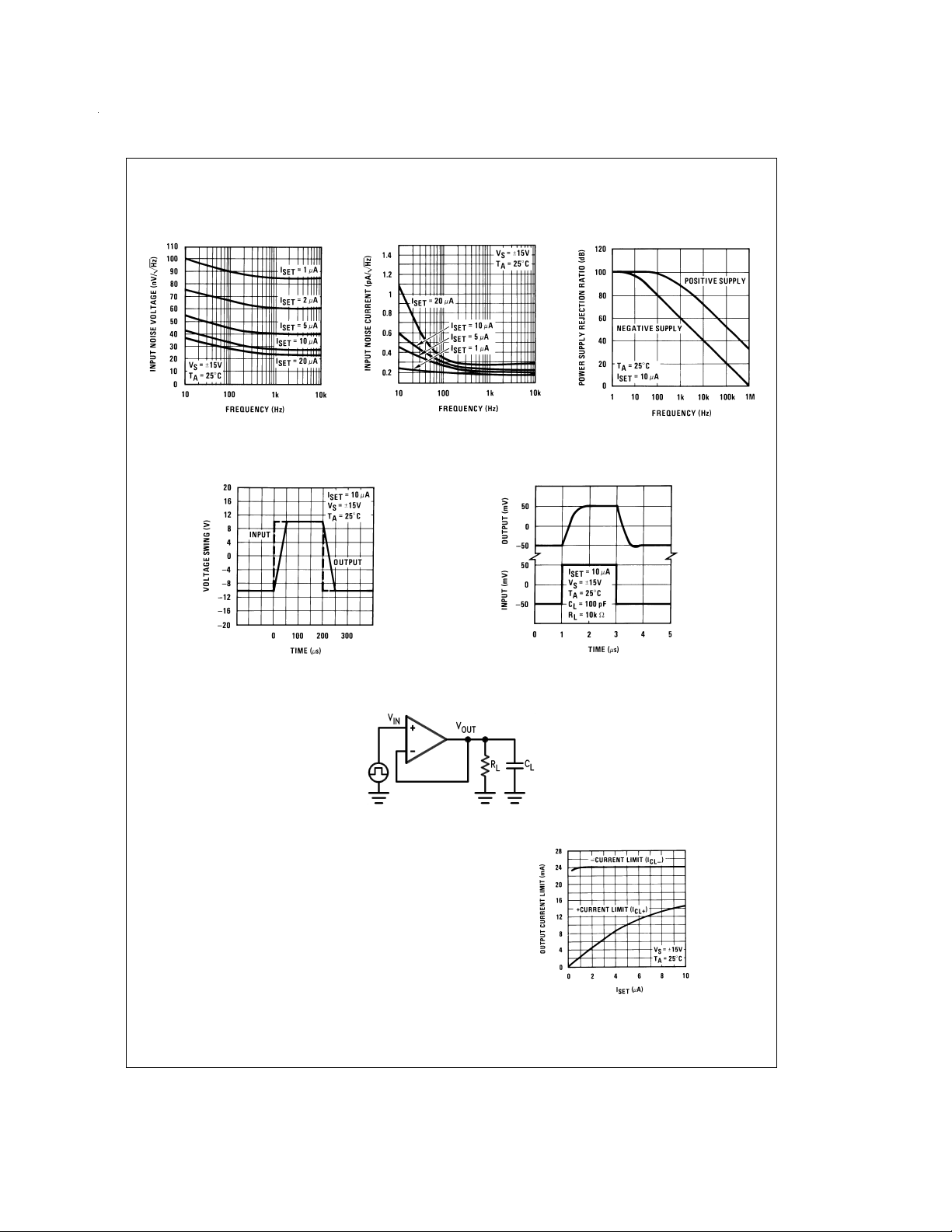
Input Noise Voltage vs
Frequency
Voltage Follower Pulse
Response
DS005654-23
Input Noise Current vs
Frequency
DS005654-26
DS005654-24
Voltage Follower Transient
Response
Power Supply Rejection
Ratio vs Frequency
DS005654-25
DS005654-27
Transient Response Test Circuit
Application Hints
Avoid reversing the power supply polarity; the device will fail.
Common-Mode Input Voltage: The negative
common-mode voltage limit is one diode drop above the
negative supply voltage. Exceeding this limit on either input
will result in an output phase reversal. The positive
common-mode limit is typically 1V below the positive supply
voltage. No output phase reversal will occur if this limit is exceeded by either input.
Output VoltageSwing vs I
swing the value oftheminimum load depends on the positive
and negative output current capability of the op amp. The
maximum available positive output current, (I
vice increases with I
(I
) is independent of I
CL−
SET
: For a desired output voltage
SET
), of the de-
whereas the negative output current
.
Figure 1
SET
CL+
illustrates the above.
DS005654-6
DS005654-7
FIGURE 1. Output Current Limit vs I
SET
www.national.com7
Page 8
Application Hints (Continued)
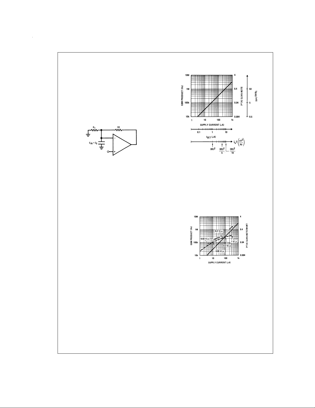
Input Capacitance: The input capacitance, C
LM146 is approximately 2 pF; any stray capacitance, C
(due to external circuit circuit layout) will add to C
resistive or active feedback is applied, an additional pole is
added to the open loop frequency response of the device.
For instance with resistive feedback (
1
curs at
⁄2π (R1||R2) (CIN+CS). Make sure that this pole oc-
Figure 2
curs at least 2 octaves beyond the expected −3 dB frequency corner of the closed loop gain of the amplifier; if not,
place a lead capacitor in the feedback such that the time
constant of this capacitor and the resistance it parallels is
equal to the R
the circuit.
I(CS+CIN
), where RIis the input resistance of
,ofthe
IN
. When
IN
), this pole oc-
power decreases proportionally and the V
stant. The usable GBW range of the op amp is 10 kHz to
3.5−4 MHz.
,
S
remains con-
OS
DS005654-9
FIGURE 2.
Temperature Effect on the GBW: The GBW (gain band-
width product), of the LM146 is directly proportional to I
and inversely proportional to the absolute temperature.
When using resistors to set the bias current, I
vice, the GBW product will decrease with increasing tem-
SET
perature. Compensation can be provided by creating an I
current directly proportional to temperature (see typical ap-
SET
, of the de-
SET
plications).
Isolation Between Amplifiers: The LM146 die is isother-
mally layed out such that crosstalk between
all 4
amplifiers is
in excess of −105 dB (DC). Optimum isolation (better than
−110 dB) occurs between amplifiers A and D, B and C; that
is, if amplifier A dissipates power on its output stage, amplifier D is the one which will be affected the least, and vice
versa. Same argument holds for amplifiers B and C.
LM146 TypicalPerformance Summary: The LM146 typical
behaviour is shown in
able. As the set current, I
current, and the supply current increase while the noise
Figure 3
. The device is fully predict-
, increases, the speed, the bias
SET
DS005654-8
FIGURE 3. LM146 Typical Characteristics
Low Power Supply Operation: The quad op amp operates
±
down to
1.3V supply. Also, since the internal circuitry is biased through programmable current sources, no degradation of the device speed will occur.
Speed vs Power Consumption: LM146 vs LM4250 (single
programmable). Through
Figure 4
, we observe that the
LM146’s power consumption has been optimized for GBW
products above 200 kHz, whereas the LM4250 will reach a
GBW of no more than 300 kHz. For GBW products below
200 kHz, the LM4250 will consume less power.
DS005654-10
FIGURE 4. LM146 vs LM4250
www.national.com 8
Page 9
Typical Applications
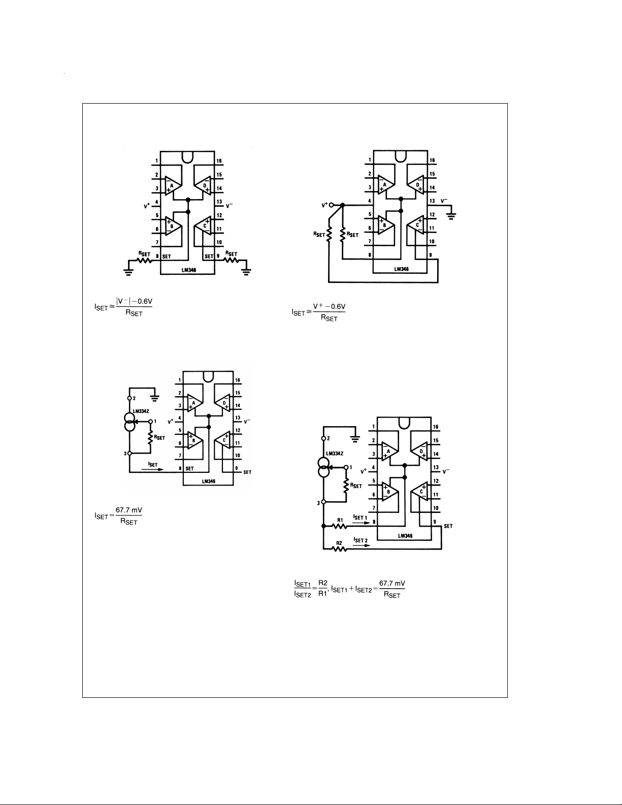
Dual Supply or Negative Supply Blasing
DS005654-39
Current Source Blasing
with Temperature Compensation
Single (Positive) Supply Blasing
DS005654-11
Blasing all 4 Amplifiers
with Single Current Source
DS005654-40
The LM334 provides an I
•
temperature. This cancels the slight GBW product Temperature coefficient
of the LM346.
directly proportional to absolute
SET
DS005654-41
≅
For I
I
•
SET1
between the 2 set currents can be tolerated.
If not, then use R1=R2 to create a 100 mV drop across these resistors.
resistors R1 and R2 are not required if a slight error
SET2
www.national.com9
Page 10
Active Filters Applications
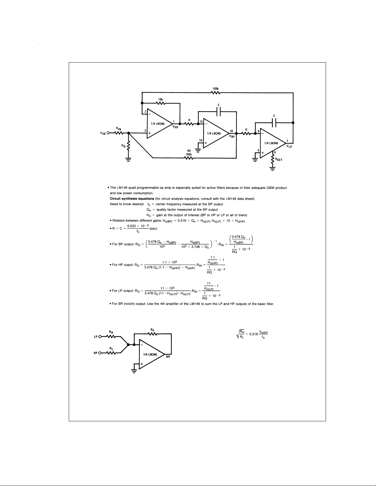
Basic (Non-Inverting “State Variable”) Active Filter Building Block
DS005654-12
Note. All resistor values are given in ohms.
DS005654-13
www.national.com 10
DS005654-33
DS005654-34
Page 11
Active Filters Applications (Continued)
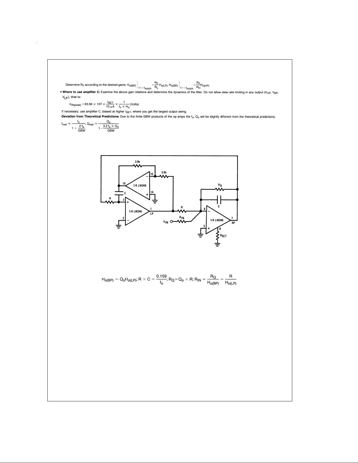
A Simple-to-Design BP, LP Filter Building Block
DS005654-35
If resistive biasing is used to set the LM346 performance, the Qoof this filter building block is nearly insensitive to the op amp’s GBW product temperature
•
drift; it has also better noise performance than the state variable filter.
DS005654-14
Circuit Synthesis Equations
For the eventual use of amplifier C, see comments on the previous page.
•
DS005654-36
www.national.com11
Page 12
Active Filters Applications (Continued)
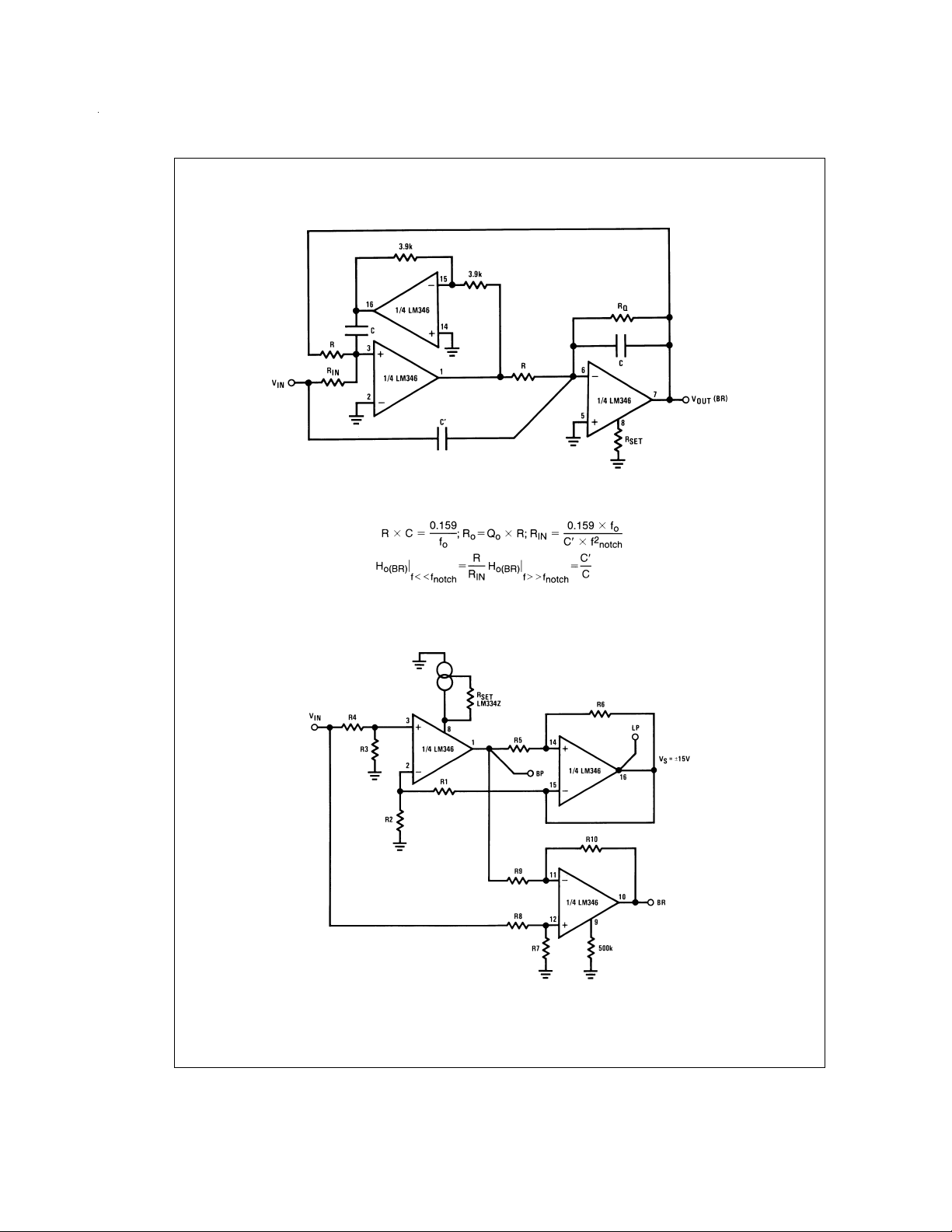
A 3-Amplifier Notch Filter (or Elliptic Filter Building Block)
Circuit Synthesis Equations
DS005654-15
For nothing but a notch output: R
•
IN
=
R, C'=C.
DS005654-37
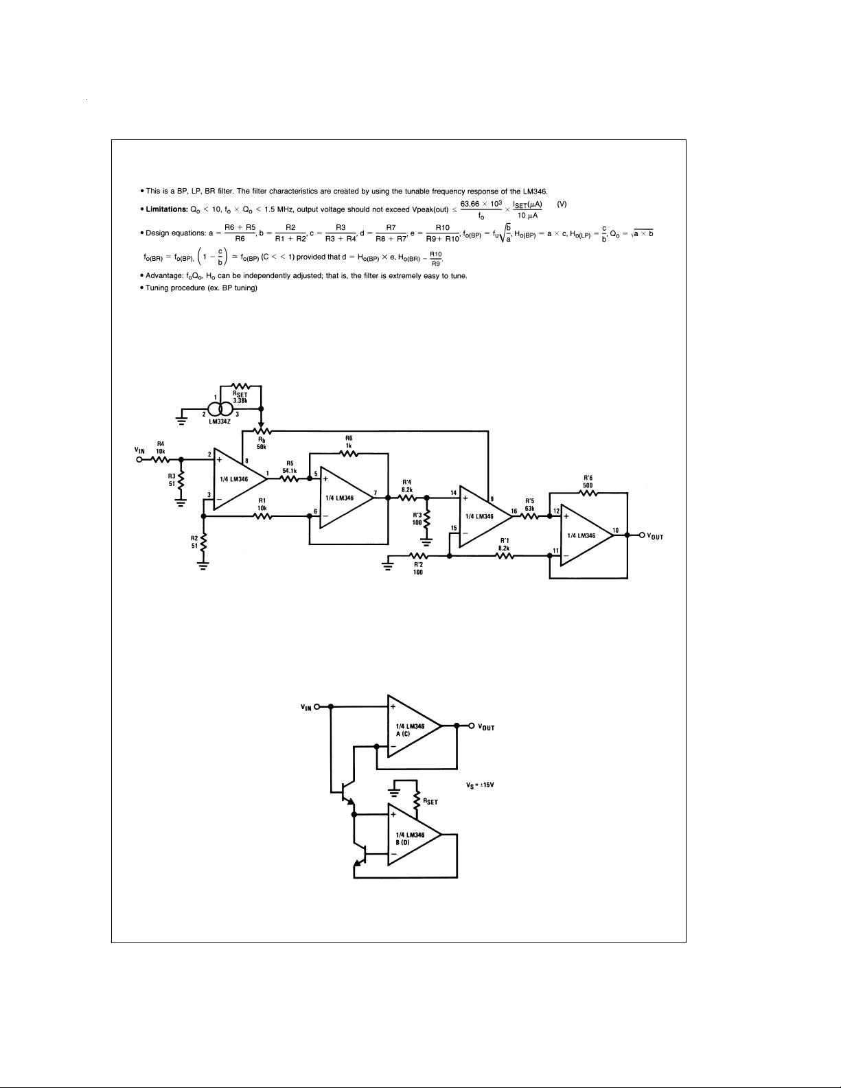
Capacitorless Active Filters (Basic Circuit)
DS005654-16
www.national.com 12
Page 13
Active Filters Applications (Continued)
1. Pick up a convenient value for b; (b<1)
2. Adjust Q
3. Adjust H
4. Adjust f
through R5
o
o(BP)
through R
o
through R4
. This adjusts the unity gain frequency (fu) of the op amp.
SET
DS005654-38
A 4th Order Butterworth Low Pass Capacitorless Filter
=
Ex: f
c
Since for this filter the GBW product of all 4 amplifiers has been designed to be the same (z1 MHz) only one current source can be used to bias the circuit.
•
Fine tuning can be further accomplished through Rb.
20 kHz, H
(gain of the filter)=1, Q
o
01
=
0.541, Q
=
1.306.
o2
DS005654-17
Miscellaneous Applications
A Unity Gain Follower
with Bias Current Reduction
For better performance, use a matched NPN pair.
•
DS005654-18
www.national.com13
Page 14
Miscellaneous Applications (Continued)
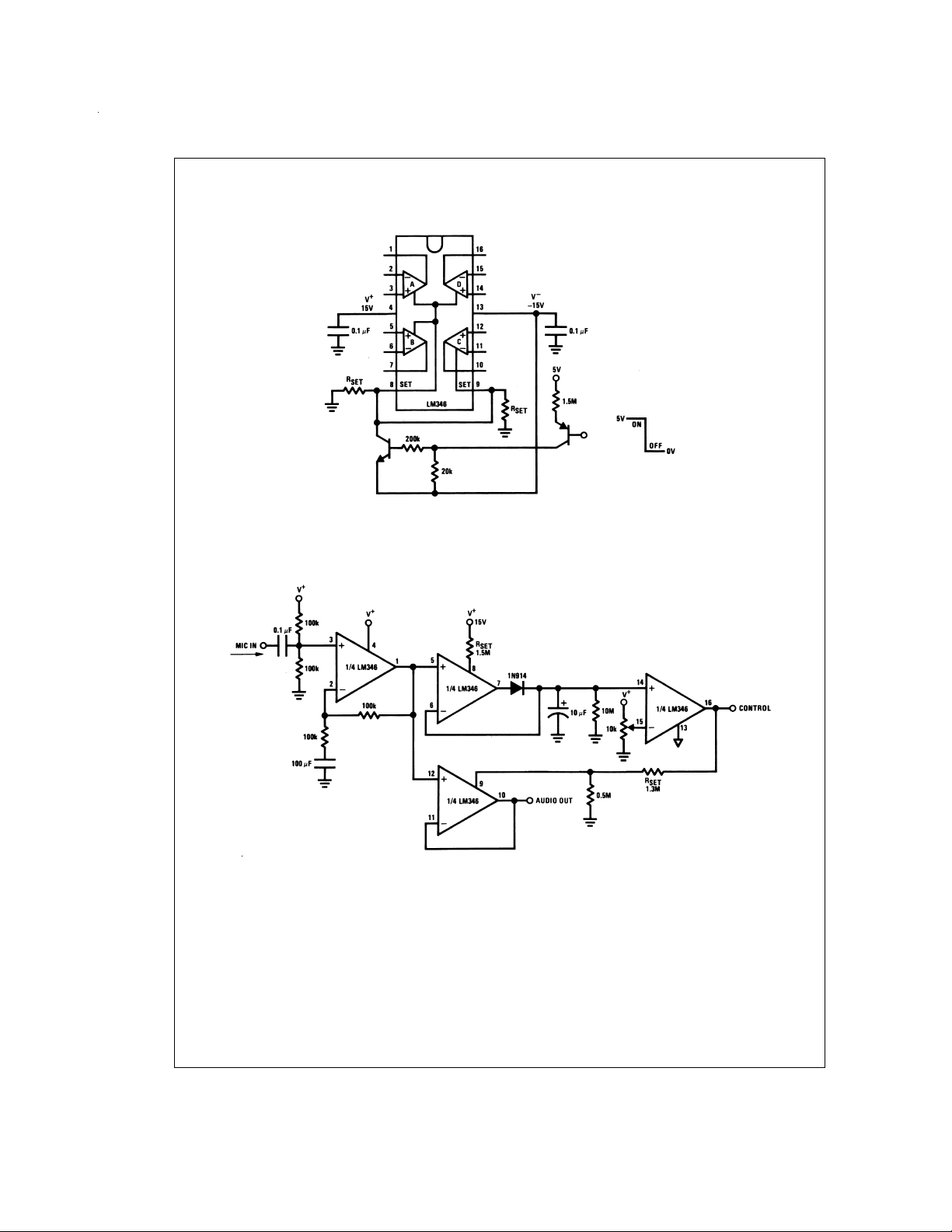
Circuit Shutdown
By pulling the SET pin(s) to V−the op amp(s) shuts down and its output goes to a high impedance state. According to this property, the LM346 can be used
•
as a very low speed analog switch.
DS005654-42
Voice Activated Switch and Amplifier
DS005654-43
www.national.com 14
Page 15
Miscellaneous Applications (Continued)
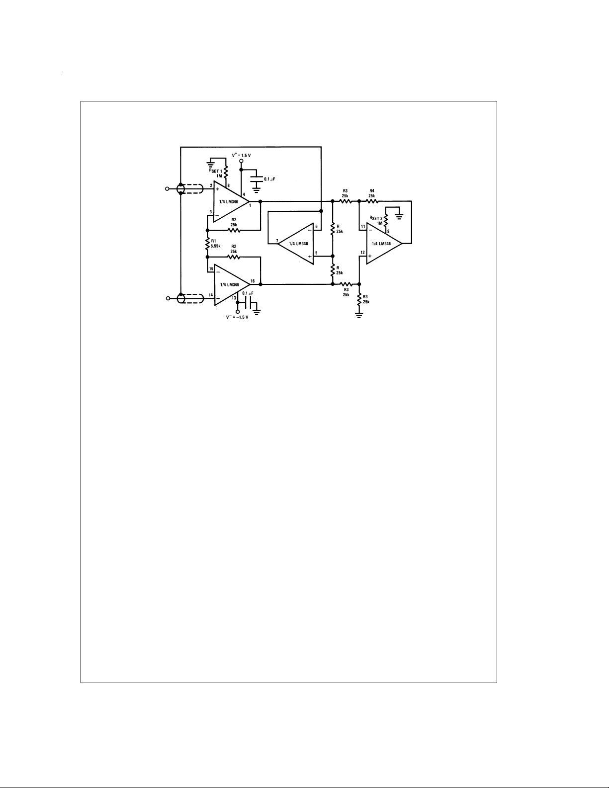
X10 Micropower Instrumentation Amplifier with Buffered Input Guarding
CMRR: 100 dB (typ)
•
Power dissipation: 0.4 mW
•
DS005654-19
www.national.com15
Page 16
Physical Dimensions inches (millimeters) unless otherwise noted
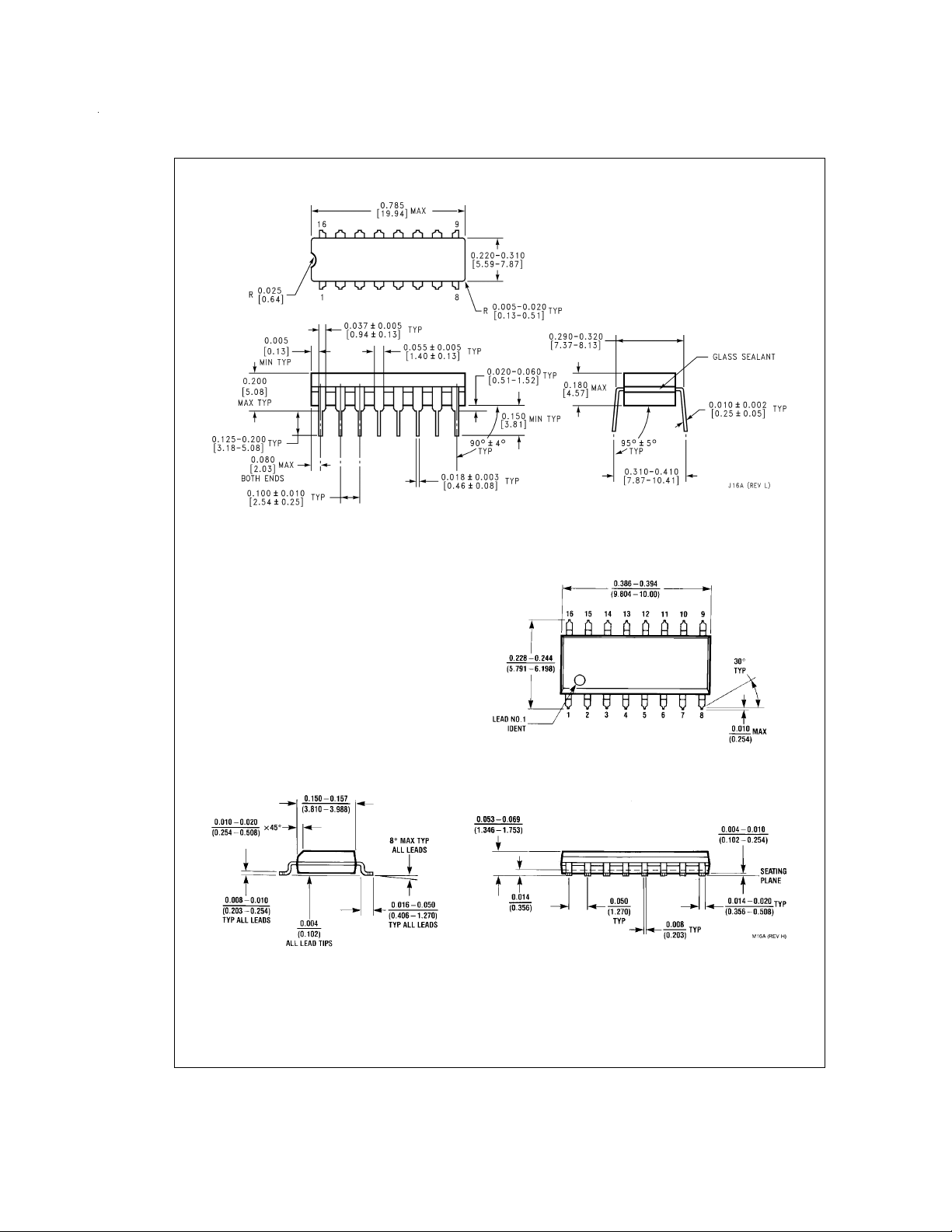
Cavity Dual-In-Line Package (J)
Order Number LM146J, LM146J/883
NS Package Number J16A
S.O. Package (M)
Order Number LM346M
NS Package Number M16A
www.national.com 16
Page 17
Physical Dimensions inches (millimeters) unless otherwise noted (Continued)
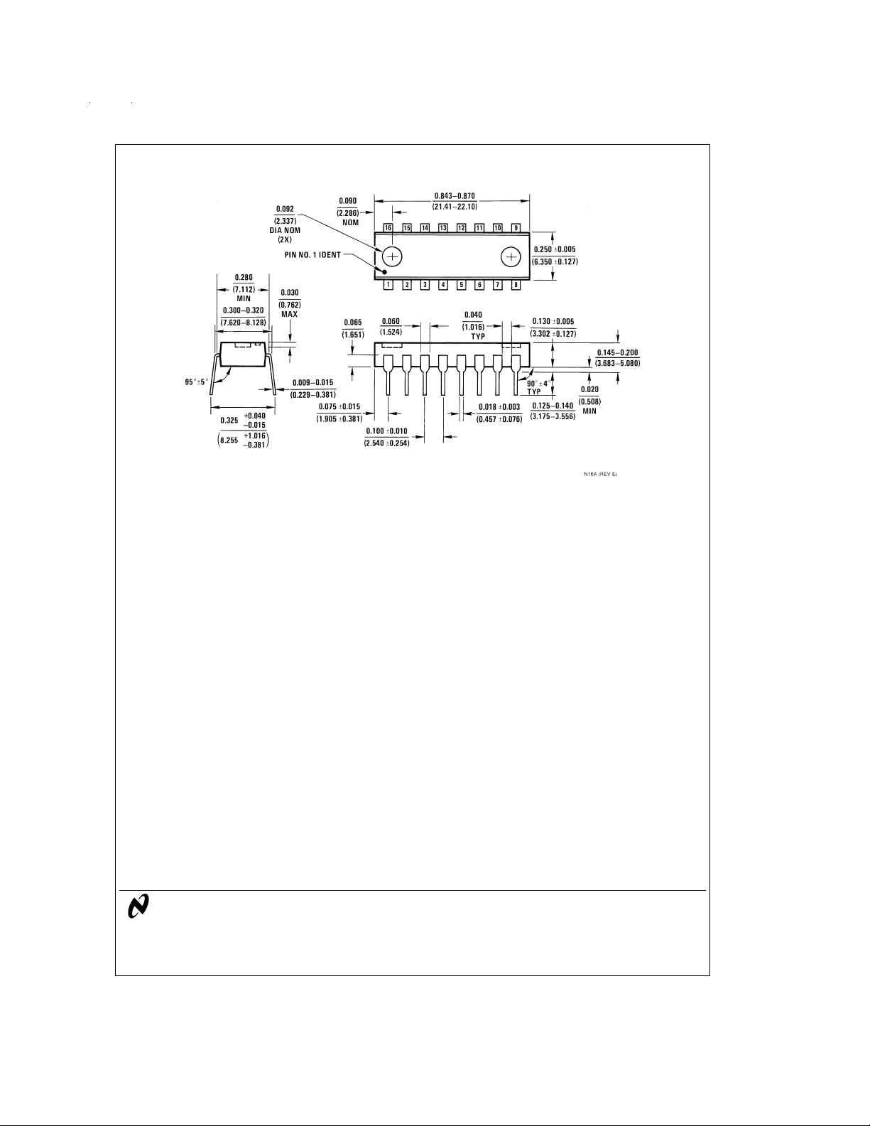
Molded Dual-In-Line Package (N)
Order Number LM346N
NS Package Number N16A
LM146/LM346 Programmable Quad Operational Amplifiers
LIFE SUPPORT POLICY
NATIONAL’S PRODUCTS ARE NOT AUTHORIZED FOR USE AS CRITICAL COMPONENTS IN LIFE SUPPORT
DEVICES OR SYSTEMS WITHOUT THE EXPRESS WRITTEN APPROVAL OF THE PRESIDENT AND GENERAL
COUNSEL OF NATIONAL SEMICONDUCTOR CORPORATION. As used herein:
1. Life support devices or systems are devices or
systems which, (a) are intended for surgical implant
into the body, or (b) support or sustain life, and
whose failure to perform when properly used in
accordance with instructions for use provided in the
2. A critical component is any component of a life
support device or system whose failure to perform
can be reasonably expected to cause the failure of
the life support device or system, or to affect its
safety or effectiveness.
labeling, can be reasonably expected to result in a
significant injury to the user.
National Semiconductor
Corporation
Americas
Tel: 1-800-272-9959
Fax: 1-800-737-7018
Email: [email protected]
www.national.com
National does not assume any responsibility for use of any circuitry described, no circuit patent licenses are implied and National reserves the right at any time without notice to change said circuitry and specifications.
National Semiconductor
Europe
Fax: +49 (0) 1 80-530 85 86
Email: [email protected]
Deutsch Tel: +49 (0) 1 80-530 85 85
English Tel: +49 (0) 1 80-532 78 32
Français Tel: +49 (0) 1 80-532 93 58
Italiano Tel: +49 (0) 1 80-534 16 80
National Semiconductor
Asia Pacific Customer
Response Group
Tel: 65-2544466
Fax: 65-2504466
Email: [email protected]
National Semiconductor
Japan Ltd.
Tel: 81-3-5639-7560
Fax: 81-3-5639-7507
 Loading...