

Page 1
LM18293 Four Channel Push-Pull Driver
General Description
The LM18293 is designed to drive DC loads up to one amp.
Typical applications include driving such inductive loads as
solenoids, relays and stepper motors along with driving
switching power transistors and use as a buffer for low level
logic signals. The four inputs accept standard TTL and DTL
levels for ease of interfacing. Two enable pins are provided
that also accept the standard TTL and DTL levels. Each
enable controls 2 channels and when an enable pin is disabled (tied low), the corresponding outputs are forced to the
TRI-STATE
condition. If the enable pins are not connected
É
(i.e., floating), the circuit will function as if it has been enabled. Separate pins are provided for the main power supply
(pin 8), and the logic supply (pin 16). This allows a lower
voltage to be used to bias up the logic resulting in reduced
power dissipation. The chip is packaged in a specially de-
Typical Connection
signed 16 pin power DIP. The 4 center pins of this package
are tied together and form the die paddle inside the package. This provides much better heat sinking capability than
most other DIP packages available. The device is capable
of operating at voltages up to 36 volts.
Features
Y
1A output current capability per channel
Y
Pin for pin replacement for L293B
Y
Special 16 pin power DIP package
Y
36 volt operation
Y
Internal thermal overload protection
Y
Logical ‘‘0’’ input voltage up to 1.5 volts results in high
noise immunity
LM18293 Four Channel Push-Pull Driver
March 1995
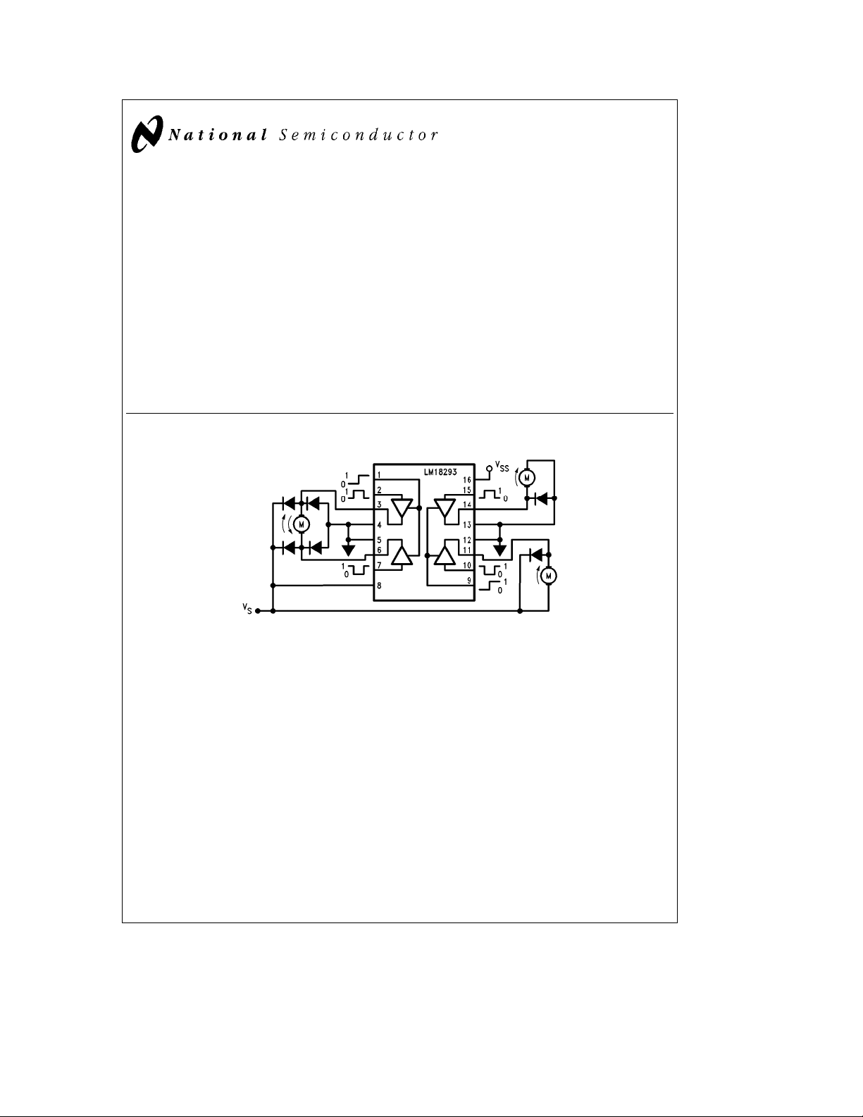
FIGURE 1. Application circuit showing bidirectional and on/off control of a single DC motor
TL/H/8706– 1
using two outputs and unidirectional on/off function of two DC motors using a single output each.
Order Number LM18293N
NS Package Number N16A
TRI-STATEÉis a registered trademark of National Semiconductor Corp.
C
1995 National Semiconductor Corporation RRD-B30M115/Printed in U. S. A.
TL/H/8706
Page 2
Absolute Maximum Ratings
If Military/Aerospace specified devices are required,
please contact the National Semiconductor Sales
Office/Distributors for availability and specifications.
Output Drive Supply Voltage (V
) 36V
S
Logic Supply Voltage (VSS) 36V
Input Voltage (V
)7V
I
Enable Voltage (VE)7V
Electrical Characteristics
e
V
24V, V
S
e
5V, Te25§C, Le0.4V, He3.5V, each channel, unless otherwise noted
SS
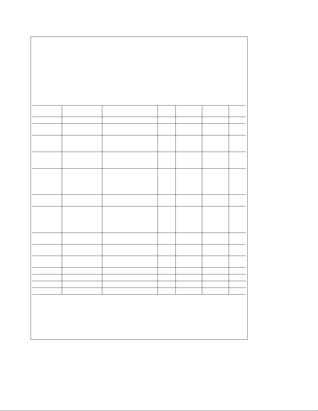
Symbol Parameter Conditions Typical
V
S
V
SS
I
S
I
SS
V
I
Main Supply (Pin 8) Maximum Supply Voltage 36 Vmax
Logic Supply (Pin 16) Minimum Logic Supply Voltage 4.5 Vmin
Maximum Logic Supply Voltage 36 Vmax
Total Quiescent V
Supply Current V
Total Quiescent Logic V
Supply Current V
(pin 16) V
e
I
e
I
e
I
e
I
e
LI
O
e
HI
O
e
LI
O
e
HI
O
Input Voltage Min Value of Low
Max Value of Low 1.5 Vmax
Peak Output Current (Non-Repetitive t
Junction Temperature (TJ)
Thermal Resistance Junction to Case (iJC)14
Thermal Resistance Junction to Ambient (iJA)80
Internal Power Dissipation Internally Limited
Operating Temperature Range
Storage Temperature Range
Lead Temperature (Solder 10 seconds) 260
Tested Limit Design Limit
(Note 1) (Note 2)
e
0V
0V
0V
0V
H 2 6 mAmax
E
e
H 16 24 mAmax
E
e
V
L 4 mAmax
E
e
H 44 60 mAmax
E
e
H 16 22 mAmax
E
e
L 16 24 mAmax
E
b
0.3 Vmin
Min Value of High 2.3 Vmin
Max Value of High (V
Max Value of High (V
I
I
V
E
Input Current V
Enable Voltage Min Value of Low
(Pins 1, 9) Max Value of Low 1.5 Vmax
e
L
I
e
V
H 30 100 mAmax
I
s
7) V
SS
l
7) 7 Vmax
SS
SS
b
10 mAmax
b
0.3 Vmin
Min Value of High 2.3 Vmin
Max Value of High (V
Max Value of High (V
I
E
Enable Current V
VCEsat Top Source Saturation I
Voltage
VCEsat Bottom Sink Saturation I
Voltage
t
r
t
f
t
on
t
off
Note 1: Tested limits are guaranteed and 100% production tested.
Note 2: Design limits are guaranteed (but not 100% production tested) over the full supply and temperature range. These limits are not used to calculate outgoing
quality levels.
Rise Time 10%– 90% V
Fall Time 90%–10% V
Turn-On Delay 50% VIto 50% V
Turn-Off Delay 50% VIto 50% V
e
L
E
e
V
H
E
eb
1 amp 1.4 1.8 Vmax
o
e
1 amp 1.2 1.8 Vmax
o
o
o
s
7) V
SS
l
7) 7 Vmax
SS
b
30
SS
b
100 mAmax
g
10 mAmax
250 ns
250 ns
o
o
450 ns
200 ns
e
5 ms) 2A
b
b
a
40§Ctoa125§C
65§Ctoa150§C
150§C
§
§
C/W
C/W
§
Units
Vmax
Vmax
C
2
Page 3
Connection Diagram
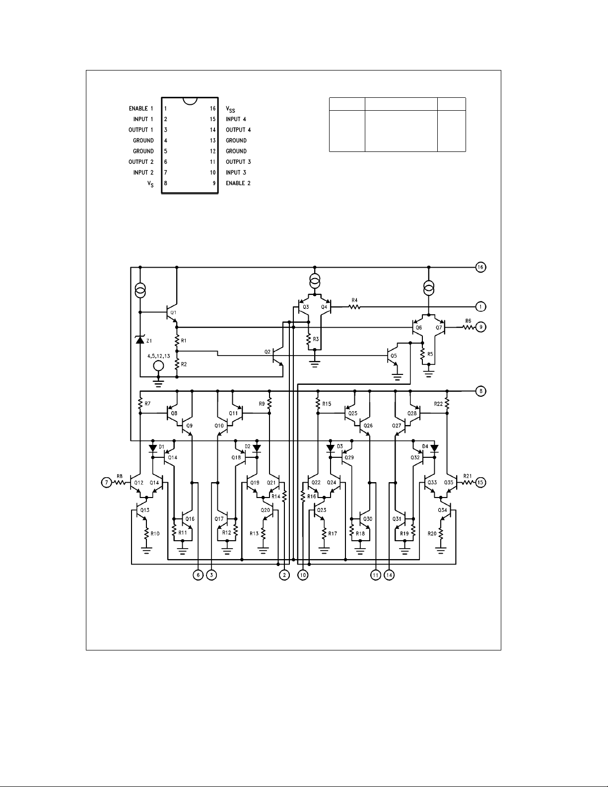
Input/Output Truth Table
Enable 1 activates outputs1&2 TL/H/8706– 2
Enable 2 activates outputs3&4
Simplified Schematic
VE(**)VI(Each Channel) V
HHH
HLL
LHX(*)
LLX(*)
(*) High output impedance.
(**) Relative to the pertinent channel.
O
TL/H/8706– 3
3
Page 4
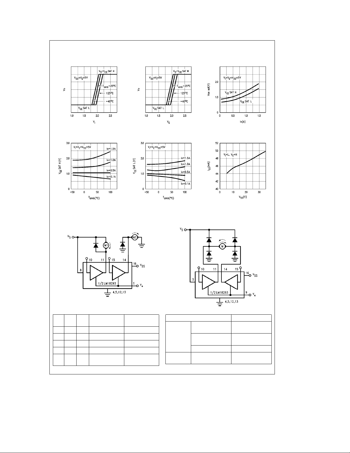
Typical Performance Characteristics V
Output Voltage vs.
Input Voltage
Output Voltage vs.
Enable Voltage
In all casese24V
S
Saturation Voltage vs.
Output Current
Source Saturation Voltage
vs. Ambient Temperature
Typical Applications
DC motor controls (with connections to
ground and to the supply voltages)
Sink Saturation Voltage
vs. Ambient Temperature
Quiescent Logic Supply
Current vs.
Logic Supply Voltage
TL/H/8706– 4
Bidirectional DC motor control
TL/H/8706– 5
Pin Pin
V
E
10 15
M1 M2
H H H Fast Motor Stop Run
H H L Fast Motor Stop Fast Motor Stop
H L H Run Run
H L L Run Fast Motor Stop
LXX
LeLow HeHigh XeDon’t care
Free Running Free Running
Motor Stop Motor Stop
Inputs Function
Pin 10eH Turn CW
Pin 15
e
V
H
E
Pin 10
Pin 15
Pin 10ePin 15 Fast Motor Stop
e
V
L Pin 10eX Free Running
E
LeLow HeHigh XeDon’t care
Pin 15eX Motor Stop
4
TL/H/8706– 6
e
L
e
L
e
H
Turn CCW
Page 5
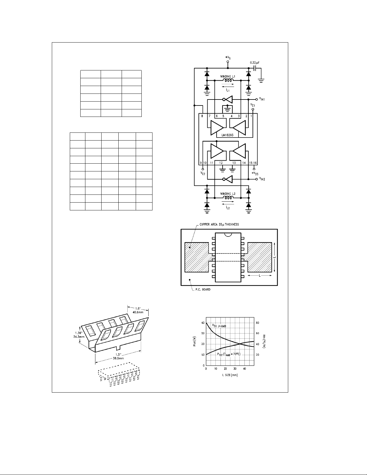
Bipolar Stepping Motor Control
Step Sequencing Tables
Full Step *
VIN1VIN2 Step
LL1
LH2
HH3
HL4
LL1
*V
1 and VE2eH
E
Half Step
VE1VE2VIN1VIN2 Step
HL L X 1
HH L L 2
LHX L 3
HH H L 4
HL H X 5
HH H H 6
LHX H 7
HH L H 8
HL L X 1
e
H
High LeLow XeDon’t care
Motor Control Block Diagram
TL/H/8706– 7
Mounting Instructions
The junction to ambient thermal resistance of the LM18293
can be reduced by soldering the ground pins to a suitable
copper area of the printed circuit board or to an external
heatsink. The graph below, which shows the maximum power dissipated and junction to ambient thermal resistance as
a function of the side ‘‘l’’ of two equal square copper areas
having a thickness of 35m, illustrates this. In addition, it is
possible to use an external heatsink (see illustration below).
During soldering the pins temperature must not exceed
230
C and the soldering time must not be longer than 12
§
seconds. The external heatsink or printed circuit copper
area must be connected to electrical ground.
Staver External Heat-sink
TL/H/8706– 10
TL/H/8706– 8
Maximum power dissipated
and junction to ambient
thermal resistance vs. size
TL/H/8706– 9
5
Page 6
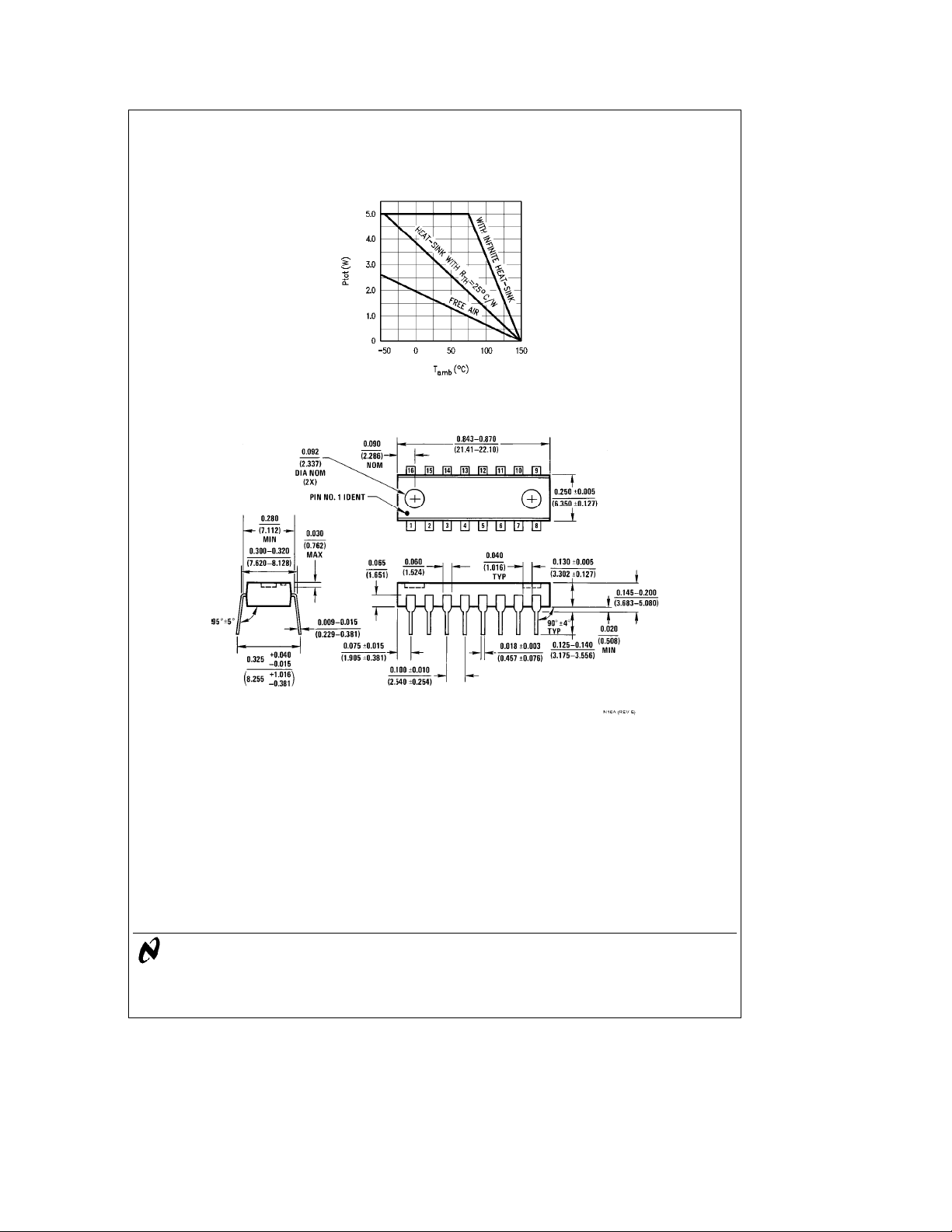
Mounting Instructions (Continued)
Maximum Allowable
Power Dissipation
vs Ambient Temperature
TL/H/8706– 11
Physical Dimensions inches (millimeters)
Lit.
LM18293 Four Channel Push-Pull Driver
Molded Dual-In-Line Package (N)
Order Number LM18293N
LIFE SUPPORT POLICY
NATIONAL’S PRODUCTS ARE NOT AUTHORIZED FOR USE AS CRITICAL COMPONENTS IN LIFE SUPPORT
DEVICES OR SYSTEMS WITHOUT THE EXPRESS WRITTEN APPROVAL OF THE PRESIDENT OF NATIONAL
SEMICONDUCTOR CORPORATION. As used herein:
1. Life support devices or systems are devices or 2. A critical component is any component of a life
systems which, (a) are intended for surgical implant support device or system whose failure to perform can
into the body, or (b) support or sustain life, and whose be reasonably expected to cause the failure of the life
failure to perform, when properly used in accordance support device or system, or to affect its safety or
with instructions for use provided in the labeling, can effectiveness.
be reasonably expected to result in a significant injury
to the user.
NS Package Number N16A
Ý
108380
National Semiconductor National Semiconductor National Semiconductor National Semiconductor
Corporation Europe Hong Kong Ltd. Japan Ltd.
1111 West Bardin Road Fax: (
Arlington, TX 76017 Email: [email protected] Ocean Centre, 5 Canton Rd. Fax: 81-043-299-2408
Tel: 1(800) 272-9959 Deutsch Tel: (
Fax: 1(800) 737-7018 English Tel: (
National does not assume any responsibility for use of any circuitry described, no circuit patent licenses are implied and National reserves the right at any time without notice to change said circuitry and specifications.
Fran3ais Tel: (
Italiano Tel: (
a
49) 0-180-530 85 86 13th Floor, Straight Block, Tel: 81-043-299-2309
a
49) 0-180-530 85 85 Tsimshatsui, Kowloon
a
49) 0-180-532 78 32 Hong Kong
a
49) 0-180-532 93 58 Tel: (852) 2737-1600
a
49) 0-180-534 16 80 Fax: (852) 2736-9960
 Loading...