

ADC78H89
7-Channel, 500 KSPS, 12-Bit A/D Converter
ADC78H89 7-Channel, 500 KSPS, 12-Bit A/D Converter
March 2005
General Description
The ADC78H89 is a low-power, seven-channel CMOS 12-bit
analog-to-digital converter with a conversion throughput of
500 KSPS. The converter is based on a successiveapproximation register architecture with an internal trackand-hold circuit. It can be configured to accept up to seven
input signals on pins AIN1 through AIN7.
The output serial data is straight binary, and is compatible
with several standards, such as SPI
™
, and many common DSP serial interfaces.
IRE
The ADC78H89 may be operated with independent analog
and digital supplies. The analog supply (AV
from +2.7V to +5.25V, and the digital supply (DV
range from +2.7V to AV
a +3V or +5V supply is 1.5 mW and 8.3 mW, respectively.
The power-down feature reduces the power consumption to
just 0.3 µW using a +3V supply, or 0.5 µW using a +5V
supply. The ADC78H89 is packaged in a 16-lead TSSOP
package. Operation over the industrial temperature range of
−40˚C to +85˚C is guaranteed.
. Normal power consumption using
DD
™
, QSPI™, MICROW-
) can range
DD
DD
) can
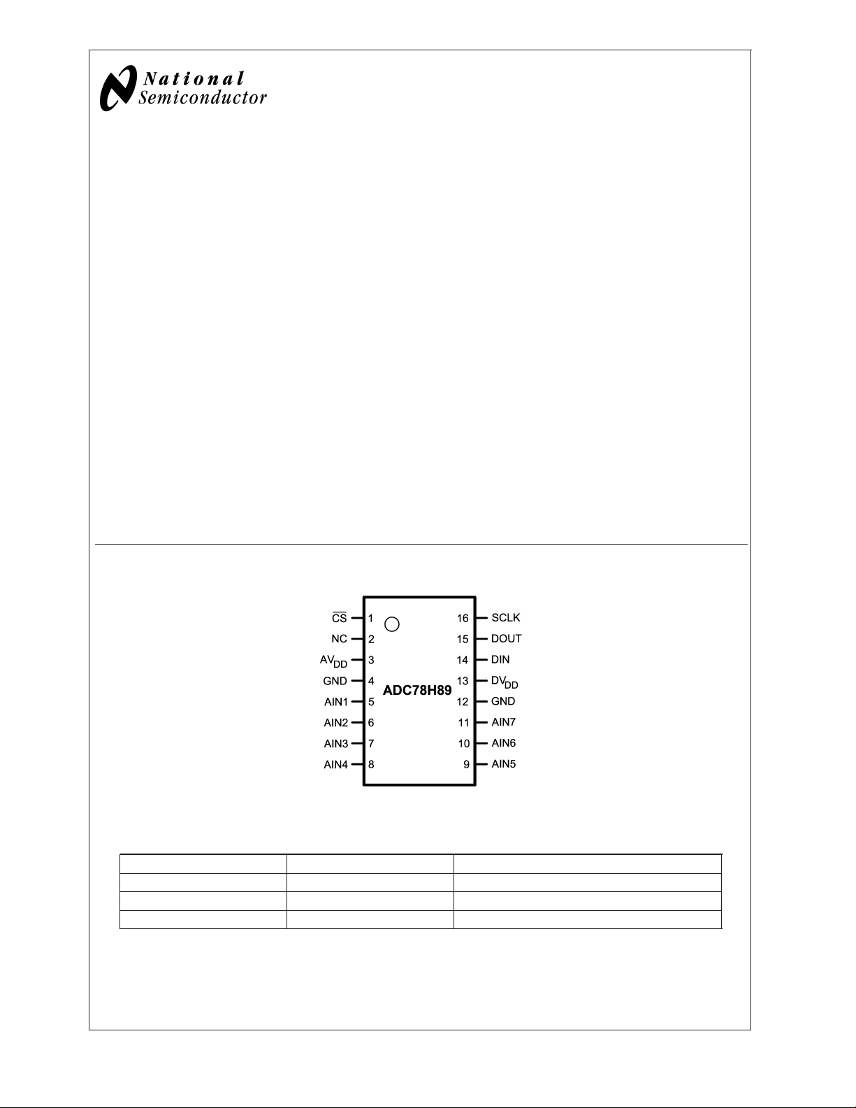
Connection Diagram
Features
n Seven input channels
n Variable power management
n Independent analog and digital supplies
™
n SPI
n Packaged in 16-lead TSSOP
/QSPI™/MICROWIRE™/DSP compatible
Key Specifications
n Conversion Rate 500 KSPS
n DNL
n INL
n Power Consumption
— 3V Supply 1.5 mW (typ)
— 5V Supply 8.3 mW (typ)
±
1 LSB (max)
±
1 LSB (max)
Applications
n Automotive Navigation
n Portable Systems
n Medical Instruments
n Mobile Communications
n Instrumentation and Control Systems
20061605
Ordering Information
Order Code Temperature Range Description
ADC78H89CIMT −40˚C to +85˚C 16-Lead TSSOP Package
ADC78H89CIMTX −40˚C to +85˚C 16-Lead TSSOP Package, Tape & Reel
ADC78H89EVAL Evaluation Board
TRI-STATE®is a trademark of National Semiconductor Corporation.
MICROWIRE
QSPI
© 2005 National Semiconductor Corporation DS200616 www.national.com
™
is a trademark of National Semiconductor Corporation.
™
and SPI™are trademarks of Motorola, Inc.
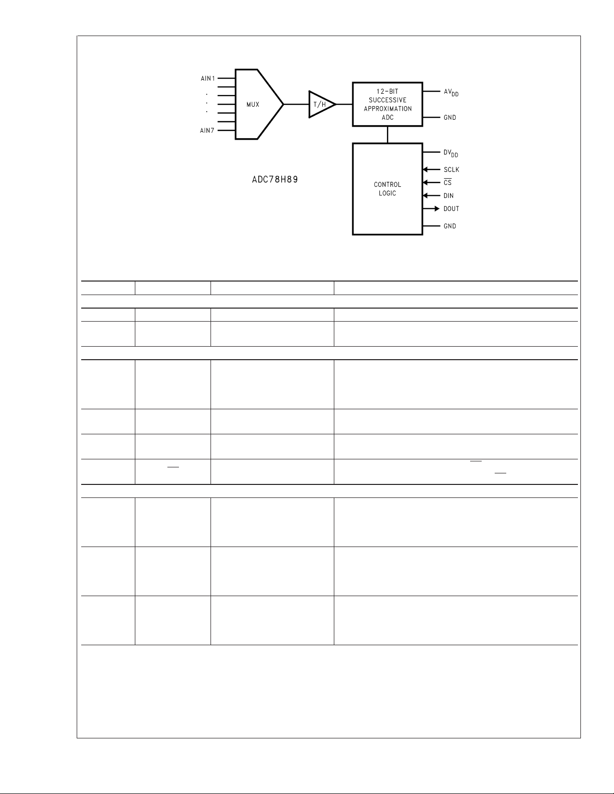
Block Diagram
ADC78H89
20061607
Pin Descriptions and Equivalent Circuits
Pin No. Symbol Equivalent Circuit Description
ANALOG I/O
5 - 11 AIN1 to AIN7 Analog inputs. These signals can range from 0V to AV
2NC
DIGITAL I/O
16 SCLK
15 DOUT
14 DIN
1CS
POWER SUPPLY
3AV
13 DV
DD
DD
4, 12 GND
This pin is not connected internally, and can be left floating,
or tied to ground.
Digital clock input. The range of frequencies for this input is
50 kHz to 8 MHz, with guaranteed performance at 8 MHz.
This clock directly controls the conversion and readout
processes.
Digital data output. The output samples are clocked out of this
pin on falling edges of the SCLK pin.
Digital data input. The ADC78H89’s Control Register is
loaded through this pin on rising edges of the SCLK pin.
Chip select. On the falling edge of CS, a conversion process
begins. Conversions continue as long as CS is held low.
Positive analog supply pin. This pin should be connected to a
quiet +2.7V to +5.25V source and bypassed to GND with 0.1
µF ceramic monolithic and 1 µF tantalum capacitors located
within 1 cm of the power pin.
Positive digital supply pin. This pin should be connected to a
+2.7V to AV
supply, and bypassed to GND with a 0.1 µF
DD
ceramic monolithic capacitor located within 1 cm of the power
pin.
The ground return for both analog and digital supplies. These
pins are tied directly together internally, so must be connected
to the same potential. If any potential exists across these
pins, large currents will flow through the device.
.
DD
www.national.com 2
ADC78H89
Absolute Maximum Ratings (Notes 1, 2)
If Military/Aerospace specified devices are required,
please contact the National Semiconductor Sales Office/
Distributors for availability and specifications.
Analog Supply Voltage AV
Digital Supply Voltage DV
DD
DD
Voltage on Any Pin to GND −0.3V to AV
−0.3V to 6.5V
−0.3V to AVDD+
0.3V, max 6.5V
DD
Operating Ratings (Notes 1, 2)
Operating Temperature Range −40˚C ≤ T
AV
Supply Voltage +2.7V to +5.25V
DD
DV
Supply Voltage +2.7V to AV
DD
Digital Input Pins Voltage Range -0.3V to AV
Clock Frequency 50 kHz to 8 MHz
Analog Input Voltage 0V to AV
+0.3V
Input Current at Any Pin (Note 3)
Package Input Current (Note 3)
Power Dissipation at T
= 25˚C See (Note 4)
A
ESD Susceptibility (Note 5)
Human Body Model
Machine Model
±
10 mA
±
20 mA
2500V
250V
Package Thermal Resistance
Package θ
16-lead TSSOP on
4-layer, 2 oz. PCB 96˚C / W
Soldering Temperature, Infrared,
10 seconds (Note 6) 260˚C
Junction Temperature +150˚C
Storage Temperature −65˚C to +150˚C
ADC78H89 Converter Electrical Characteristics (Note 8)
The following specifications apply for AVDD=DVDD= +2.7V to 5.25V, f
noted. Boldface limits apply for T
A=TMIN
to T
: all other limits TA= 25˚C.
MAX
Symbol Parameter Conditions Typical Limits
STATIC CONVERTER CHARACTERISTICS
Resolution with No Missing Codes AV
INL Integral Non-Linearity AV
DNL Differential Non-Linearity AV
OE Offset Error AV
OEM Offset Error Match AV
GE Gain Error AV
GEM Gain Error Match AV
= +5.0V, DVDD= +3.3V 12 Bits
DD
= +5.0V, DVDD= +3.3V
DD
= +5.0V, DVDD= +3.3V
DD
= +5.0V, DVDD= +3.3V
DD
= +5.0V, DVDD= +3.3V
DD
= +5.0V, DVDD= +3.3V
DD
= +5.0V, DVDD= +3.3V
DD
DYNAMIC CONVERTER CHARACTERISTICS
AV
= +5.0V, DVDD= +3.0V,
SINAD Signal-to-Noise Plus Distortion Ratio
SNR Signal-to-Noise Ratio
THD Total Harmonic Distortion
SFDR Spurious-Free Dynamic Range
ENOB Effective Number of Bits
Channel-to-Channel Crosstalk
Intermodulation Distortion, Second
IMD
Order Terms
Intermodulation Distortion, Third
Order Terms
FPBW -3 dB Full Power Bandwidth
DD
= 40.2 kHz, −0.02 dBFS
f
IN
AV
= +5.0V, DVDD= +3.0V,
DD
= 40.2 kHz, −0.02 dBFS
f
IN
AV
= +5.0V, DVDD= +3.0V,
DD
= 40.2 kHz, −0.02 dBFS
f
IN
AV
= +5.0V, DVDD= +3.0V,
DD
= 40.2 kHz, −0.02 dBFS
f
IN
AV
= +5.0V, DVDD= +3.0V,
DD
= 40.2 kHz, −0.02 dBFS
f
IN
AV
= +5.0V, DVDD= +3.0V,
DD
= 40.2 kHz
f
IN
AV
= +5.0V, DVDD= +3.0V,
DD
= 40.161 kHz, fb= 41.015 kHz
f
a
AV
= +5.0V, DVDD= +3.0V,
DD
= 40.161 kHz, fb= 41.015 kHz
f
a
AV
= +5V 11 MHz
DD
AV
= +3V 8 MHz
DD
SCLK
= 8 MHz, f
= 500 KSPS unless otherwise
SAMPLE
±
±
±
±
±
±
72.6 dB
72.8 dB
-86 dB
88 dB
11.8 bits
-82 dB
-93 dB
-90 dB
≤ +85˚C
A
DD
DD
DD
JA
Units
(Note 7)
1 LSB (max)
1 LSB (max)
2 LSB (max)
2 LSB (max)
3 LSB (max)
3 LSB (max)
www.national.com3
ADC78H89 Converter Electrical Characteristics (Note 8) (Continued)
The following specifications apply for AVDD=DVDD= +2.7V to 5.25V, f
noted. Boldface limits apply for T
A=TMIN
to T
: all other limits TA= 25˚C.
MAX
ADC78H89
Symbol Parameter Conditions Typical Limits
ANALOG INPUT CHARACTERISTICS
V
IN
I
DCL
C
INA
DIGITAL INPUT CHARACTERISTICS
V
IH
V
IL
I
IN
C
IND
DIGITAL OUTPUT CHARACTERISTICS
V
OH
V
OL
I
OZH
I
OZL
C
OUT
POWER SUPPLY CHARACTERISTICS (C
AV
DD
DV
DD
I
DD
P
D
AC ELECTRICAL CHARACTERISTICS
f
SCLK
f
S
t
CONV
DC Duty Cycle 50
t
ACQ
f
RATE
t
AD
Input Range 0 to AV
DC Leakage Current
Input Capacitance
Input High Voltage
In Track Mode 33 pF
In Hold Mode 3 pF
= +4.75Vto +5.25V 2.4 V (min)
DV
DD
DV
= +2.7V to +3.6V 2.1 V (min)
DD
Input Low Voltage DVDD= +2.7V to +5.25V 0.8 V (max)
Input Current VIN=0VorDV
DD
Input Capacitance 2 4 pF (max)
Output High Voltage
Output Low Voltage I
,
TRI-STATE Leakage Current
I
SOURCE
DV
SINK
= 200 µA,
= +2.7V to +5.25V
DD
= 200 µA 0.4 V (max)
TRI-STATE Output Capacitance 2 4 pF (max)
Output Coding Straight (Natural) Binary
=10pF)
L
,
Analog and Digital Supply Voltages AVDD≥ DV
DD
AVDD=DVDD= +4.75V to +5.25V,
Total Supply Current, Normal Mode
(Operational, CS low)
Total Supply Current, Shutdown (CS
high)
Power Consumption, Normal Mode
(Operational, CS low)
Power Consumption, Shutdown (CS
high)
f
AV
f
AV
f
AV
f
AVDD=DVDD= +4.75V to +5.25V 8.3 12 mW (max)
AV
AV
AV
= 500 KSPS, fIN=40kHz
SAMPLE
=DVDD= +2.7V to +3.6V,
DD
= 500 KSPS, fIN=40kHz
SAMPLE
=DVDD= +4.75V to +5.25V,
DD
= 0 KSPS
SAMPLE
=DVDD= +2.7V to +3.6V,
DD
= 0 KSPS
SAMPLE
=DVDD= +2.7V to +3.6V 1.5 8.3 mW (max)
DD
=DVDD= +4.75V to +5.25V 0.5 µW
DD
=DVDD= +2.7V to +3.6V 0.3 µW
DD
Maximum Clock Frequency 8 MHz (max)
Minimum Clock Frequency 50 kHz
Maximum Sample Rate 500 KSPS (min)
Conversion Time 13 13 SCLK cycles
Track/Hold Acquisition Time Full-Scale Step Input 3 SCLK cycles
Throughput Time Conversion Time + Acquisition Time 16 SCLK cycles
Throughput Rate 500 KSPS (min)
Aperture Delay 4 ns
SCLK
= 8 MHz, f
= 500 KSPS unless otherwise
SAMPLE
DD
±
0.01 1 µA (max)
1.65 2.3 mA (max)
0.5 2.3 mA (max)
0.1 µA
0.1 µA
±
1 µA (max)
DV
−0.5 V (min)
DD
±
1 µA (max)
2.7 V (min)
5.25 V (max)
40 % (min)
60 % (max)
Units
(Note 7)
V
www.national.com 4
ADC78H89 Timing Specifications
The following specifications apply for AVDD=DVDD= +2.7V to 5.25V, f
T
A=TMIN
to T
: all other limits TA= 25˚C.
MAX
Symbol Parameter Conditions Typical Limits Units
t
SCLK High to CS Fall Setup Time (Note 10) 10 ns (min)
1a
t
SCLK Low to CS Fall Hold Time (Note 10) 10 ns (min)
1b
Delay from CS Until DOUT
t
2
TRI-STATE®Disabled
Data Access Time after SCLK
t
3
Falling Edge
Data Setup Time Prior to SCLK
t
4
Rising Edge
t
Data Valid SCLK Hold Time 10 ns (max)
5
t
SCLK High Pulse Width
6
t
SCLK Low Pulse Width
7
CS Rising Edge to DOUT
t
8
High-Impedance
Note 1: Absolute maximum ratings are limiting values which indicate limits beyond which damage to the device may occur. Operating Ratings indicate conditions
for which the device is functional, but do not guarantee specific performance limits. For guaranteed specifications and test conditions, see the Electrical
Characteristics. The guaranteed specifications apply only for the test conditions listed. Some performance characteristics may degrade when the device is not
operated under the listed test conditions.
Note 2: All voltages are measured with respect to GND = 0V, unless otherwise specified.
Note 3: When the input voltage at any pin exceeds the power supplies (that is, V
The 50 mA maximum package input current rating limits the number of pins that can safely exceed the power supplies with an input current of 10 mA to five.
Note 4: The absolute maximum junction temperature (T
junction-to-ambient thermal resistance (θ
for maximum power dissipation listed above will be reached only when the ADC78H89 is operated in a severe fault condition (e.g. when input or output pins are
driven beyond the power supply voltages, or the power supply polarity is reversed). Obviously, such conditions should always be avoided.
Note 5: Human body model is 100 pF capacitor discharged through a 1.5 kΩ resistor. Machine model is 220 pF discharged through ZERO ohms.
Note 6: See AN450, “Surface Mounting Methods and Their Effect on Product Reliability”, or the section entitled “Surface Mount” found in any post 1986 National
Semiconductor Linear Data Book, for other methods of soldering surface mount devices.
Note 7: Tested limits are guaranteed to National’s AOQL (Average Outgoing Quality Level).
Note 8: Data sheet min/max specification limits are guaranteed by design, test, or statistical analysis.
Note 9: Except power supply pins.
Note 10: Clock may be in any state (high or low) when CS is asserted, with the restrictions on setup and hold time given by t
), and the ambient temperature (TA), and can be calculated using the formula PDMAX=(TJmax − TA)/θJA. The values
JA
max) for this device is 150˚C. The maximum allowable power dissipation is dictated by TJmax, the
J
<
IN
AGND or V
= 8 MHz, CL=50pF,Boldface limits apply for
SCLK
30 ns (max)
30 ns (max)
10 ns (max)
0.4 x
t
SCLK
0.4 x
t
SCLK
20 ns (max)
>
VAor VD), the current at that pin should be limited to 10 mA.
IN
and t1b.
1a
ns (min)
ns (min)
ADC78H89
www.national.com5
 Loading...