September 19, 2008
ADC161S626
16-Bit, 50 to 250 kSPS, Differential Input, MicroPower ADC
ADC161S626 16-Bit, 50 to 250 kSPS, Differential Input, MicroPower ADC
General Description
The ADC161S626 is a 16-bit successive-approximation register (SAR) Analog-to-Digital converter (ADC) with a maximum sampling rate of 250 kSPS. The ADC161S626 has a
minimum signal span accuracy of ± 0.003% over the temperate range of −40°C to +85°C. The converter features a differential analog input with an excellent common-mode signal
rejection ratio of 85 dB, making the ADC161S626 suitable for
noisy environments.
The ADC161S626 operates with a single analog supply (VA)
and a separate digital input/output (VIO) supply. VA can range
from +4.5V to +5.5V and VIO can range from +2.7V to +5.5V.
This allows a system designer to maximize performance and
minimize power consumption by operating the analog portion
of the ADC at a VA of +5V while interfacing with a +3.3V controller. The serial data output is binary 2's complement and is
SPI™ compatible.
The performance of the ADC161S626 is guaranteed over
temperature at clock rates of 1 MHz to 5 MHz and reference
voltages of +2.5V to +5.5V. The ADC161S626 is available in
a small 10-lead MSOP package. The high accuracy, differential input, low power consumption, and small size make the
ADC161S626 ideal for direct connection to bridge sensors
and transducers in battery operated systems or remote data
acquisition applications.
Applications
Direct Sensor Interface
■
I/O Modules
■
Data Acquisition
■
Portable Systems
■
Motor Control
■
Medical Instruments
■
Instrumentation and Control Systems
■
Features
16-bit resolution with no missing codes
■
Guaranteed performance from 50 to 250 kSPS
■
±0.003% signal span accuracy
■
Separate Digital Input/Output Supply
■
True differential input
■
External voltage reference range of +0.5V to V
■
Zero-Power Track Mode with 0 µsec wake-up delay
■
Wide input common-mode voltage range of 0V to V
■
SPI™/QSPI™/MICROWIRE™ compatible Serial
■
Interface
Operating temperature range of −40°C to +85°C
■
Small MSOP-10 package
■
A
Key Specifications
Conversion Rate 50 kSPS to 250 kSPS
■
DNL + 0.8 / − 0.5 LSB
■
INL ± 0.8 LSB
■
Offset Error Temp Drift 2.5 µV/°C
■
Gain Error Temp Drift 0.3 ppm/°C
■
SNR 93.2 dBc
■
THD − 104 dBc
■
■
Power Consumption
■
10 kSPS, 5V 0.24 mW
—
■
200 kSPS, 5V 5.3 mW
—
250 kSPS, 5V 5.8 mW
—
Power-Down, 5V 10 µW
—
A
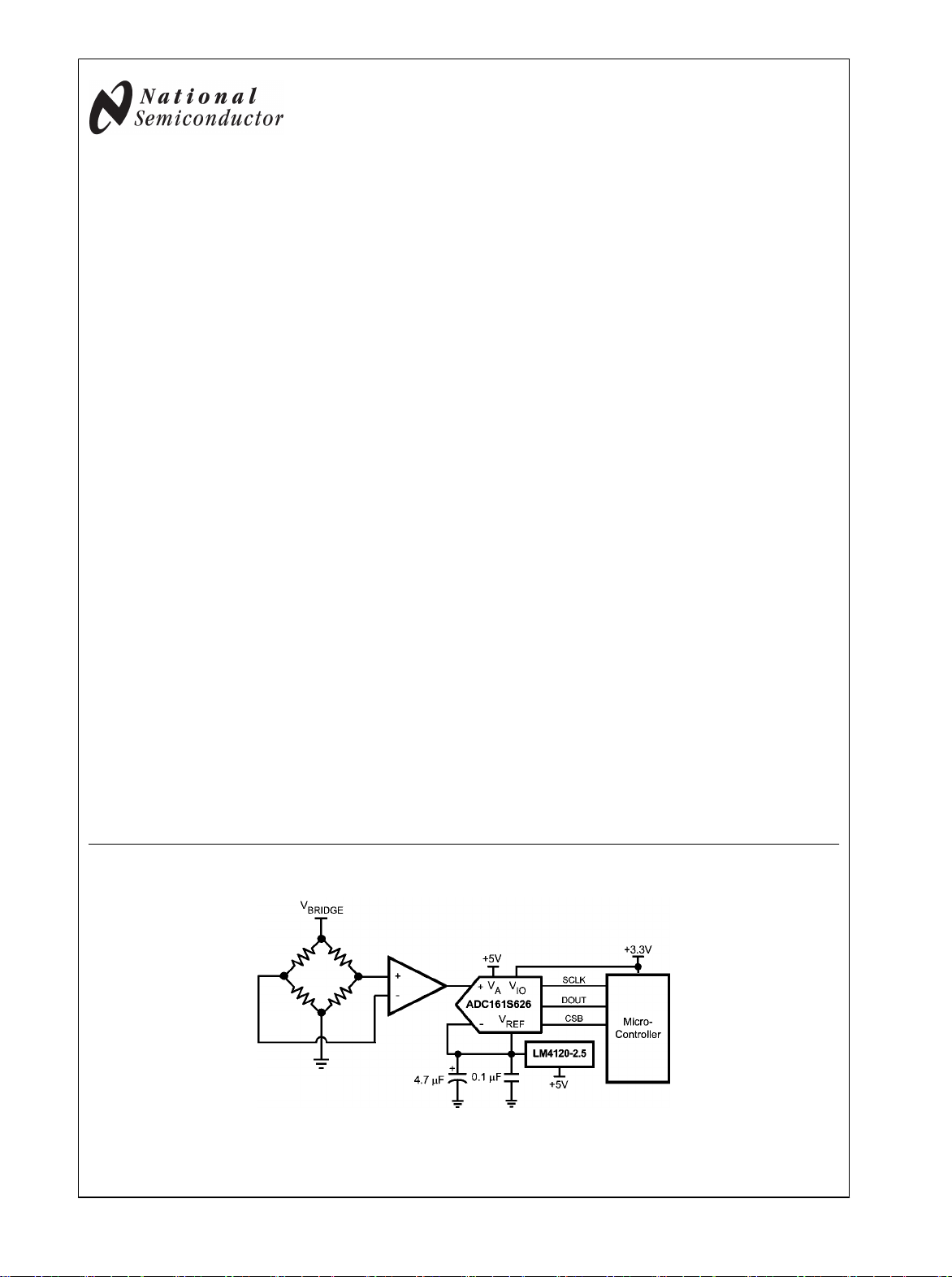
Typical Application
30073482
TRI-STATE® is a trademark of National Semiconductor Corporation.
MICROWIRE™ is a trademark of National Semiconductor Corporation.
QSPI™ and SPI™ are trademarks of Motorola, Inc.
© 2008 National Semiconductor Corporation 300734 www.national.com
Ordering Information
Order Code Temperature Range Description Top Mark
ADC161S626CIMM −40°C to +85°C 10-Lead MSOP Package, 1000 Units Tape & Reel X98C
ADC161S626
ADC161S626CIMMX −40°C to +85°C 10-Lead MSOP Package, 3500 Units Tape & Reel X98C
ADC161S626EB Evaluation Board
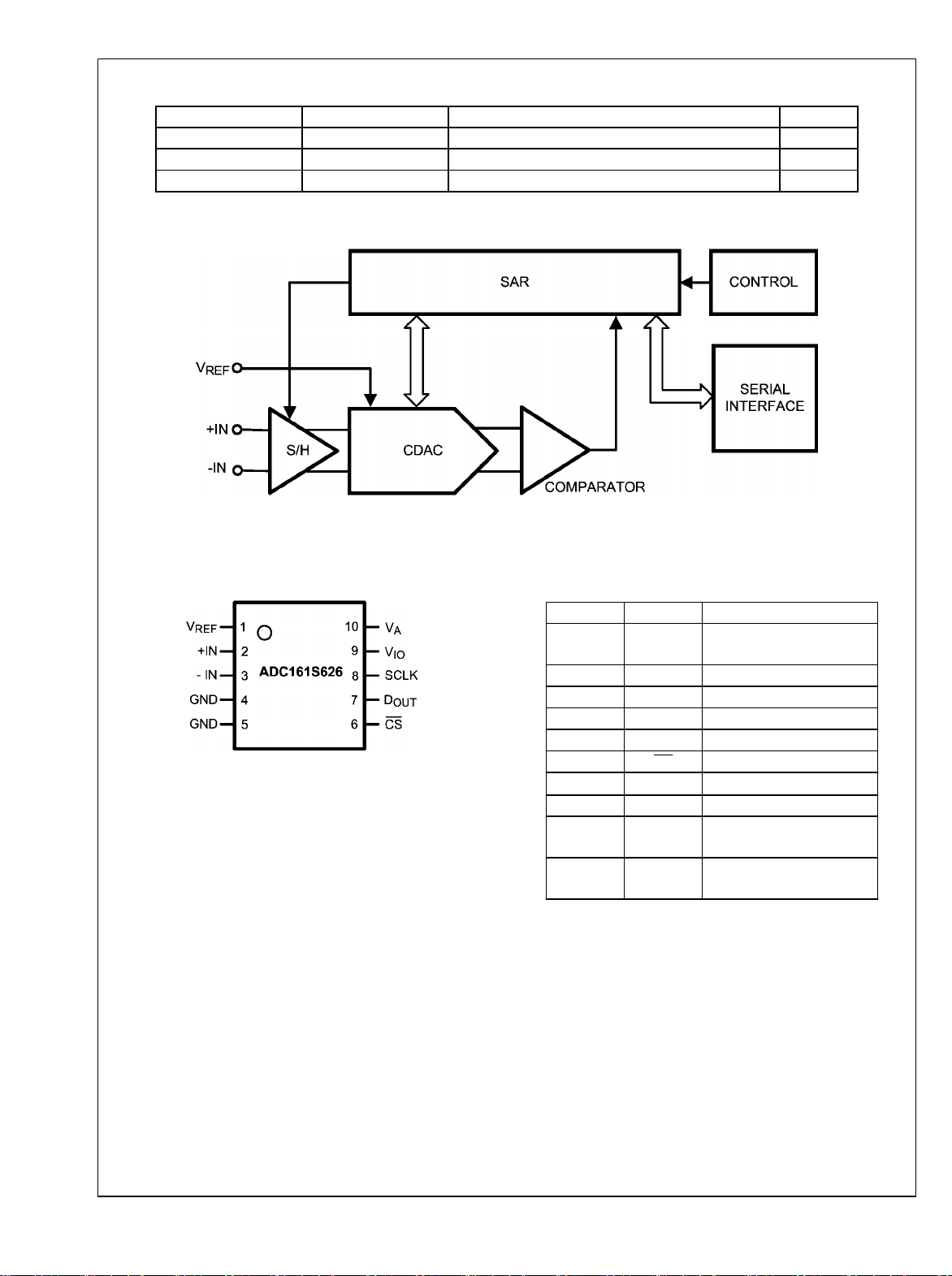
Block Diagram
30073402
Connection Diagram
30073405
Pin Descriptions
Pin No. Symbol Description
1
V
2 +IN Non-Inverting Input
3 −IN Inverting Input
4 GND Ground
5 GND Ground
6 CS Chip Select Bar
7
D
8 SCLK Serial Clock
9
10
V
V
Voltage Reference
REF
+0.5V < V
Serial Data Output
OUT
Digital Input/Output Power
IO
+2.7V < V
Analog Power
A
+4.5V < V
REF
REF
REF
< V
A
< +5.5V
< +5.5V
www.national.com 2
ADC161S626
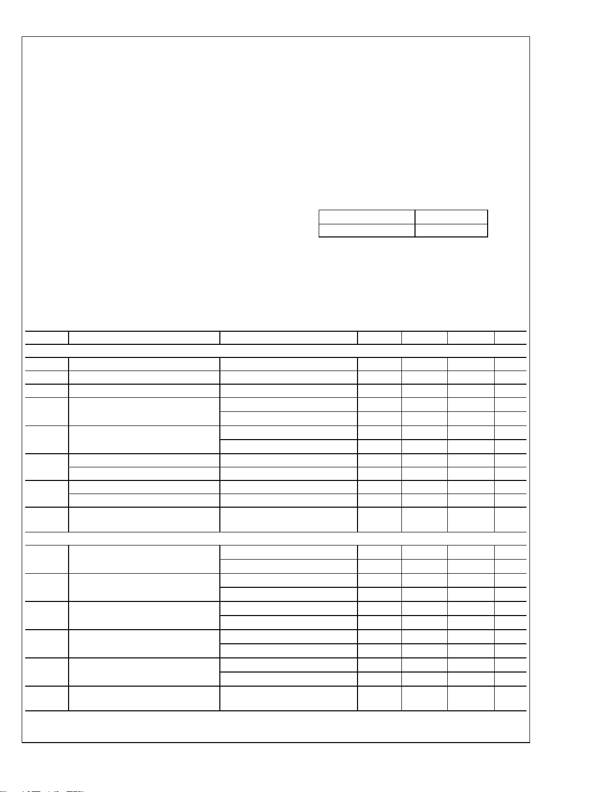
Absolute Maximum Ratings (Notes 1, 2)
If Military/Aerospace specified devices are required,
please contact the National Semiconductor Sales Office/
Distributors for availability and specifications.
Analog Supply Voltage V
Digital I/O Supply Voltage V
A
IO
Voltage on Any Analog Input Pin to
GND
Voltage on Any Digital Input Pin to
GND
Input Current at Any Pin (Note 3) ±10 mA
Package Input Current (Note 3) ±50 mA
Power Consumption at TA = 25°C
ESD Susceptibility (Note 5)
Human Body Model
Machine Model
Charge Device Model
Junction Temperature +150°C
Storage Temperature −65°C to +150°C
−0.3V to 6.5V
−0.3V to 6.5V
−0.3V to (VA + 0.3V)
−0.3V to (VIO + 0.3V)
See (Note 4)
2500V
250V
1250V
Operating Ratings (Notes 1, 2)
Operating Temperature Range
Supply Voltage, V
Supply Voltage, V
Reference Voltage, V
A
IO
REF
Analog Input Pins Voltage Range 0V to V
Differential Analog Input Voltage −V
Input Common-Mode Voltage, VCMSee Figure 10 (Sect 2.3)
Digital Input Pins Voltage Range 0V to V
Clock Frequency 1 MHz to 5 MHz
−40°C ≤ TA ≤ +85°C
+4.5V to +5.5V
+2.7V to +5.5V
+0.5V to V
to +V
REF
REF
Package Thermal Resistance
Package
10-lead MSOP 240°C / W
Soldering process must comply with National
Semiconductor's Reflow Temperature Profile specifications.
Refer to www.national.com/packaging. (Note 6)
θ
JA
IO
ADC161S626 Converter Electrical Characteristics (Note 7)
The following specifications apply for VA = 4.5V to 5.5V, VIO = 2.7V to 5.5V, and V
or V
= 4.5V to 5.5V for f
REF
values apply for TA = T
= 1 MHz to 5 MHz; fIN = 20 kHz, and CL = 25 pF, unless otherwise noted. Maximum and minimum
SCLK
to T
MIN
; the typical values are tested at TA = 25°C.
MAX
Symbol Parameter Conditions Min Typ Max Units
STATIC CONVERTER CHARACTERISTICS
Resolution with No Missing Codes 16 Bits
DNL Differential Non-Linearity −1 -0.5/+0.8 +2 LSB
INL Integral Non-Linearity −2 ±0.8 +2 LSB
V
= 2.5V
OE Offset Error
OE
FSE
GE
GE
DRIFT
DRIFT
Offset Error Temperature Drift
Positive Full-Scale Error −0.003 ±0.03 %FS
Negative Full-Scale Error −0.002 ±0.03 %FS
Positive Gain Error −0.002 ±0.02 %FS
Negative Gain Error −0.0001 ±0.02 %FS
Gain Error Temperature Drift 0.3
V
V
V
REF
REF
REF
REF
= 5V
= 2.5V
= 5V
DYNAMIC CONVERTER CHARACTERISTICS
V
= 2.5V
SINAD Signal-to-Noise Plus Distortion Ratio
SNR Signal-to-Noise Ratio
THD Total Harmonic Distortion
SFDR Spurious-Free Dynamic Range
ENOB Effective Number of Bits
FPBW −3 dB Full Power Bandwidth
REF
V
= 4.5V to 5.5V
REF
V
= 2.5V
REF
V
= 4.5V to 5.5V
REF
V
= 2.5V
REF
V
= 4.5V to 5.5V
REF
V
= 2.5V
REF
V
= 4.5V to 5.5V
REF
V
= 2.5V
REF
V
= 4.5V to 5.5V
REF
Output at 70.7%FS with FS
Differential Input
= 2.5V to 5.5V for f
REF
= 1 MHz to 4 MHz
SCLK
−1 −0.1 +1 mV
−0.4 mV
3.7 µV/°C
2.5 µV/°C
85 88 dBc
89 93.0 dBc
85 88 dBc
89 93.2 dBc
−104 dBc
−106 dBc
108 dBc
111 dBc
13.8 14.3 bits
14.5 15.2 bits
26 MHz
ppm/°
C
A
A
3 www.national.com
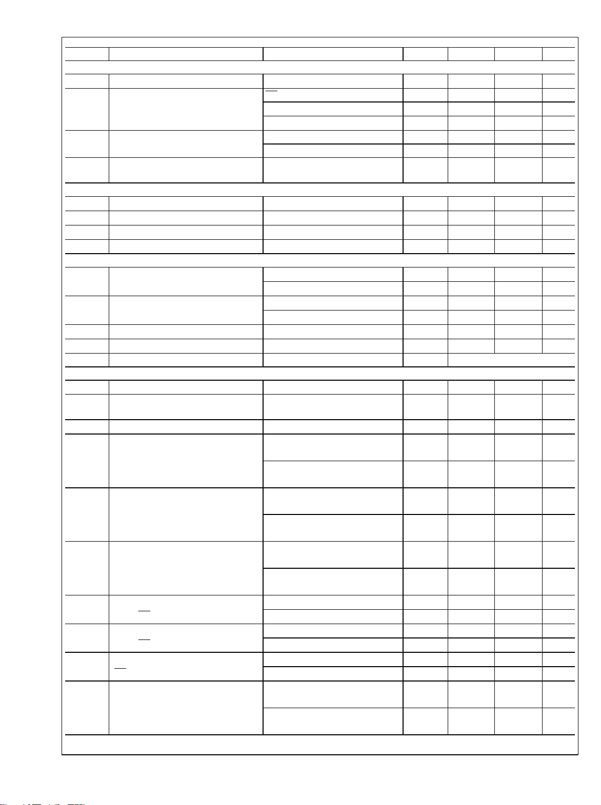
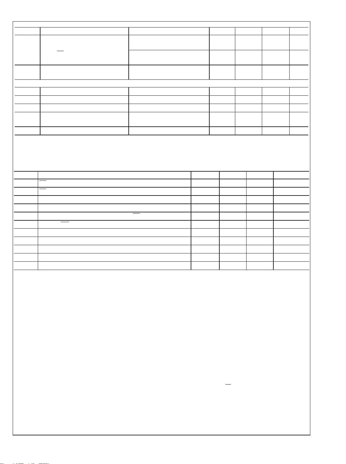
Symbol Parameter Conditions Min Typ Max Units
ANALOG INPUT CHARACTERISTICS
V
IN
ADC161S626
I
INA
C
INA
Differential Input Range
Analog Input Current
Input Capacitance (+IN or −IN)
CMRR Common Mode Rejection Ratio
CS high ±1 µA
V
= 5V, VIN = 0V, fS = 50 kSPS
REF
V
= 5V, VIN = 0V, fS = 200 kSPS
REF
In Acquisition Mode 20 pF
In Conversion Mode 4 pF
See the Specification Definitions for
the test condition
−V
REF
+V
REF
3.2 nA
10.3 nA
85 dB
DIGITAL INPUT CHARACTERISTICS
V
V
I
C
IND
IH
IL
IND
Input High Voltage
Input Low Voltage
Digital Input Current ±1 µA
Input Capacitance 4 pF
fIN = 0 Hz 0.7 x V
fIN = 0 Hz
1.7
IO
1.9 V
0.3 x V
DIGITAL OUTPUT CHARACTERISTICS
V
V
I
OZH
C
OH
OL
OUT
Output High Voltage
Output Low Voltage
, I
TRI-STATE Leakage Current
OZL
TRI-STATE Output Capacitance
= 200 µA VIO − 0.2 VIO − 0.03
SOURCE
I
= 1 mA
SOURCE
I
= 200 µA
SOURCE
I
= 1 mA
SOURCE
Force 0V or V
Force 0V or V
A
A
0.07 V
4 pF
VIO − 0.09
0.01 0.4 V
±1 µA
V
V
I
Output Coding Binary 2'S Complement
POWER SUPPLY CHARACTERISTICS
V
A
V
IO
V
REF
IVA (Conv)
I
VIO
(Conv)
I
VREF
(Conv)
IVA (PD)
I
(PD)
VIO
I
VREF
PWR
(Conv)
Analog Supply Voltage Range 4.5 5 5.5 V
Digital Input/Output Supply Voltage
Range
(Note 9) 2.7 3 5.5 V
Reference Voltage Range 0.5 5
Analog Supply Current, Conversion
Mode
Digital I/O Supply Current, Conversion
Mode
Reference Current, Conversion Mode
Analog Supply Current, Power Down
Mode (CS high)
Digital I/O Supply Current, Power Down
Mode (CS high)
Reference Current, Power Down Mode
(PD)
(CS high)
Power Consumption, Conversion Mode
VA = 5V, f
fS = 200 kSPS
VA = 5V, f
fS = 250 kSPS
VIO = 3V, f
fS = 200 kSPS
VIO = 3V, f
fS = 250 kSPS
VA = 5V, f
fS = 200 kSPS
VA = 5V, f
fS = 250 kSPS
f
= 5 MHz, VA = 5V
SCLK
f
= 0 Hz, VA = 5V (Note 8)
SCLK
f
= 5 MHz, VIO = 3V
SCLK
f
= 0 Hz, VIO = 3V (Note 8)
SCLK
f
= 5 MHz, V
SCLK
f
= 0 Hz, V
SCLK
VA = 5V, f
kSPS, and fIN = 20 kHz,
VA = 5V, f
kSPS, and fIN = 20
= 4 MHz,
SCLK
= 5 MHz,
SCLK
= 4 MHz,
SCLK
= 5 MHz,
SCLK
= 4 MHz,
SCLK
= 5 MHz,
SCLK
= 5V
REF
= 5V (Note 8)
REF
= 4 MHz, fS = 200
SCLK
= 5 MHz, fS = 250
SCLK
1060 µA
1160 1340 µA
80 µA
100 µA
80 µA
100 170 µA
7 µA
2 3 µA
1 µA
0.3 0.5 µA
0.5 µA
0.5 0.7 µA
5.3 mW
5.8 6.7 mW
V
A
V
V
IO
V
www.national.com 4
Symbol Parameter Conditions Min Typ Max Units
f
= 5 MHz, VA = 5.0V
PWR (PD)
Power Consumption, Power Down
Mode (CS high)
PSRR Power Supply Rejection Ratio
SCLK
(Note 8)
f
= 0 Hz, VA = 5.0V
SCLK
(Note 8)
See the Specification Definitions for
the test condition
35 µW
10 15 µW
−78 dB
AC ELECTRICAL CHARACTERISTICS
f
SCLK
f
S
t
ACQ
t
CONV
t
AD
Maximum Clock Frequency 1 5 MHz
Maximum Sample Rate (Note 10) 50 250 kSPS
Acquisition/Track Time 600 ns
Conversion/Hold Time 17
SCLK
cycles
Aperture Delay See the Specification Definitions 6 ns
ADC161S626 Timing Specifications (Note 7)
The following specifications apply for VA = 4.5V to 5.5V, VIO = 2.7V to 5.5V, V
25 pF, unless otherwise noted. Maximum and minimum values apply for TA = T
25°C.
Symbol Parameter Min Typ Max Units
t
t
CS Setup Time prior to an SCLK rising edge 8 3 ns
CSS
CS Hold Time after an SCLK rising edge 8 3
CSH
t
D
DH
t
DA
t
DIS
t
CS
t
EN
t
CH
t
CL
t
r
t
f
Hold Time after an SCLK falling edge
OUT
D
Access Time after an SCLK falling edge
OUT
D
Disable Time after the rising edge of CS (Note 11)
OUT
Minimum CS Pulse Width 20 ns
D
Enable Time after the 2nd falling edge of SCLK
OUT
SCLK High Time 20 ns
SCLK Low Time 20 ns
D
Rise Time
OUT
D
Fall Time
OUT
= 2.5V to 5.5V, f
REF
to T
MIN
MAX
; the typical values are tested at TA =
= 1Mz to 5MHz, and CL =
SCLK
6 11 ns
18 41 ns
20 30 ns
20 70 ns
7 ns
7 ns
ADC161S626
Note 1: Absolute Maximum Ratings indicate limits beyond which damage to the device may occur. Operating Ratings indicate conditions for which the device is
functional, but do not guarantee specific performance limits. For guaranteed specifications and test conditions, see the Electrical Characteristics. The guaranteed
specifications apply only for the test conditions listed. Some performance characteristics may degrade when the device is not operated under the listed test
conditions. Operation of the device beyond the maximum Operating Ratings is not recommended.
Note 2: All voltages are measured with respect to GND = 0V, unless otherwise specified.
Note 3: When the input voltage at any pin exceeds the power supplies (that is, VIN < GND or VIN > VA), the current at that pin should be limited to 10 mA. The 50
mA maximum package input current rating limits the number of pins that can safely exceed the power supplies with an input current of 10 mA to five.
Note 4: The absolute maximum junction temperature (TJmax) for this device is 150°C. The maximum allowable power dissipation is dictated by TJmax, the
junction-to-ambient thermal resistance (θJA), and the ambient temperature (TA), and can be calculated using the formula PDMAX = (TJmax − TA)/θJA. The values
for maximum power dissipation listed above will be reached only when the ADC161S626 is operated in a severe fault condition (e.g. when input or output pins
are driven beyond the power supply voltages, or the power supply polarity is reversed). Such conditions should always be avoided.
Note 5: Human body model is a 100 pF capacitor discharged through a 1.5 kΩ resistor. Machine model is a 220 pF capacitor discharged through 0 Ω. Charge
device model simulates a pin slowly acquiring charge (such as from a device sliding down the feeder in an automated assembler) then rapidly being discharged.
Note 6: Reflow temperature profiles are different for lead-free packages.
Note 7: Typical values are at TJ = 25°C and represent most likely parametric norms. Test limits are guaranteed to National's AOQL (Average Outgoing Quality
Level).
Note 8: This parameter is guaranteed by design and/or characterization and is not tested in production.
Note 9: The value of VIO is independent of the value of VA. For example, VIO could be operating at 5.5V while VA is operating at 4.5V or VIO could be operating
at 2.7V while VA is operating at 5.5V.
Note 10: While the maximum sample rate is f
Note 11: t
is the time for D
DIS
to change 10% while being loaded by the Timing Test Circuit.
OUT
/ 20, the actual sample rate may be lower than this by having the CS rate slower than f
SCLK
5 www.national.com
SCLK
/ 20.
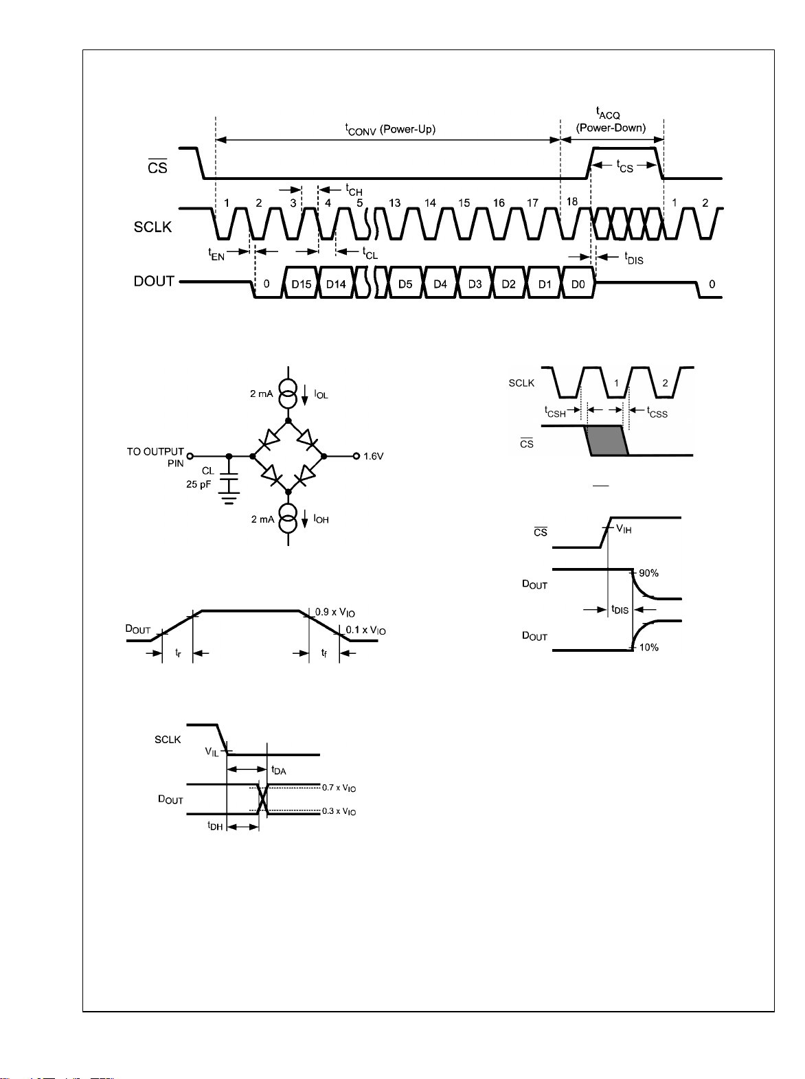
Timing Diagrams
ADC161S626
30073401
FIGURE 1. ADC161S626 Single Conversion Timing Diagram
30073410
FIGURE 2. Timing Test Circuit
FIGURE 3. D
FIGURE 4. D
Rise and Fall Times
OUT
Hold and Access Times
OUT
30073411
30073408
30073406
FIGURE 5. Valid CS Assertion Times
30073412
FIGURE 6. Voltage Waveform for t
DIS
www.national.com 6
ADC161S626
Specification Definitions
APERTURE DELAY is the time between the first falling edge
of SCLK and the time when the input signal is sampled for
conversion.
COMMON MODE REJECTION RATIO (CMRR) is a measure
of how well in-phase signals common to both input pins are
rejected.
To calculate CMRR, the change in output offset is measured
while the common mode input voltage is changed from 2V to
3V.
CMRR = 20 LOG ( Δ Common Input / Δ Output Offset)
CONVERSION TIME is the time required, after the input voltage is acquired, for the ADC to convert the input voltage to a
digital word.
DIFFERENTIAL NON-LINEARITY (DNL) is the measure of
the maximum deviation from the ideal step size of 1 LSB.
DUTY CYCLE is the ratio of the time that a repetitive digital
waveform is high to the total time of one period. The specification here refers to the SCLK.
EFFECTIVE NUMBER OF BITS (ENOB, or EFFECTIVE
BITS) is another method of specifying Signal-to-Noise and
Distortion or SINAD. ENOB is defined as (SINAD − 1.76) /
6.02 and says that the converter is equivalent to a perfect
ADC of this (ENOB) number of bits.
FULL POWER BANDWIDTH is a measure of the frequency
at which the reconstructed output fundamental drops 3 dB
below its low frequency value for a full scale input.
GAIN ERROR is the deviation from the ideal slope of the
transfer function. It is the difference between Positive FullScale Error and Negative Full-Scale Error and can be calculated as:
Gain Error = Positive Full-Scale Error − Negative Full-Scale
INTEGRAL NON-LINEARITY (INL) is a measure of the deviation of each individual code from a line drawn from ½ LSB
below the first code transition through ½ LSB above the last
code transition. The deviation of any given code from this
straight line is measured from the center of that code value.
MISSING CODES are those output codes that will never appear at the ADC outputs. The ADC161S626 is guaranteed not
to have any missing codes.
NEGATIVE FULL-SCALE ERROR is the difference between
the differential input voltage at which the output code transitions from code 0x8001h to 0x8000h and −V
NEGATIVE GAIN ERROR is the difference between the negative full-scale error and the offset error.
Error
+ 1 LSB.
REF
OFFSET ERROR is the difference between the differential
input voltage at which the output code transitions from code
0x0000h to 0x0001h and 1 LSB.
POSITIVE FULL-SCALE ERROR is the difference between
the differential input voltage at which the output code transitions from code 0xFFFEh to 0xFFFFh and V
POSITIVE GAIN ERROR is the difference between the positive full-scale error and the offset error.
POWER SUPPLY REJECTION RATIO (PSRR) is a measure
of how well a change in the analog supply voltage is rejected.
PSRR is calculated from the ratio of the change in offset error
for a given change in supply voltage, expressed in dB. For the
ADC161S626, VA is changed from 4.5V to 5.5V.
PSRR = 20 LOG (ΔOutput Offset / ΔVA)
SIGNAL TO NOISE RATIO (SNR) is the ratio, expressed in
dB, of the rms value of the input signal to the rms value of the
sum of all other spectral components below one-half the sampling frequency, not including harmonics or d.c.
SIGNAL TO NOISE PLUS DISTORTION (S/N+D or
SINAD) Is the ratio, expressed in dB, of the rms value of the
input signal to the rms value of all of the other spectral components below one-half the sampling frequency, including
harmonics but excluding d.c.
SPURIOUS FREE DYNAMIC RANGE (SFDR) is the difference, expressed in dB, between the desired signal amplitude
to the amplitude of the peak spurious spectral component below one-half the sampling frequency, where a spurious spectral component is any signal present in the output spectrum
that is not present at the input and may or may not be a harmonic.
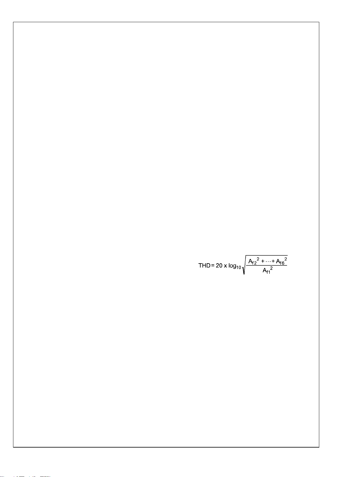
TOTAL HARMONIC DISTORTION (THD) is the ratio of the
rms total of the first five harmonic components at the output
to the rms level of the input signal frequency as seen at the
output, expressed in dB. THD is calculated as
where Af1 is the RMS power of the input frequency at the output and Af2 through Af6 are the RMS power in the first 5
harmonic frequencies.
THROUGHPUT TIME is the minimum time required between
the start of two successive conversion.
- 1 LSB.
REF
7 www.national.com
 Loading...