

February 21, 2008
ADC12DS105
Dual 12-Bit, 105 MSPS A/D Converter with Serial LVDS
Outputs
ADC12DS105 Dual 12-Bit, 105 MSPS A/D Converter with Serial LVDS Outputs
General Description
The ADC12DS105 is a high-performance CMOS analog-todigital converter capable of converting two analog input signals into 12-bit digital words at rates up to 105 Mega Samples
Per Second (MSPS). The digital outputs are serialized and
provided on differential LVDS signal pairs. This converter uses a differential, pipelined architecture with digital error correction and an on-chip sample-and-hold circuit to minimize
power consumption and the external component count, while
providing excellent dynamic performance. The ADC12DS105
may be operated from a single +3.0V or 3.3V power supply.
A power-down feature reduces the power consumption to
very low levels while still allowing fast wake-up time to full
operation. The differential inputs accept a 2V full scale differential input swing. A stable 1.2V internal voltage reference is
provided, or the ADC12DS105 can be operated with an external 1.2V reference. The selectable duty cycle stabilizer
maintains performance over a wide range of clock duty cycles. A serial interface allows access to the internal registers
for full control of the ADC12DS105's functionality. The ADC12DS105 is available in a 60-lead LLP package and operates over the industrial temperature range of −40°C to +85°C
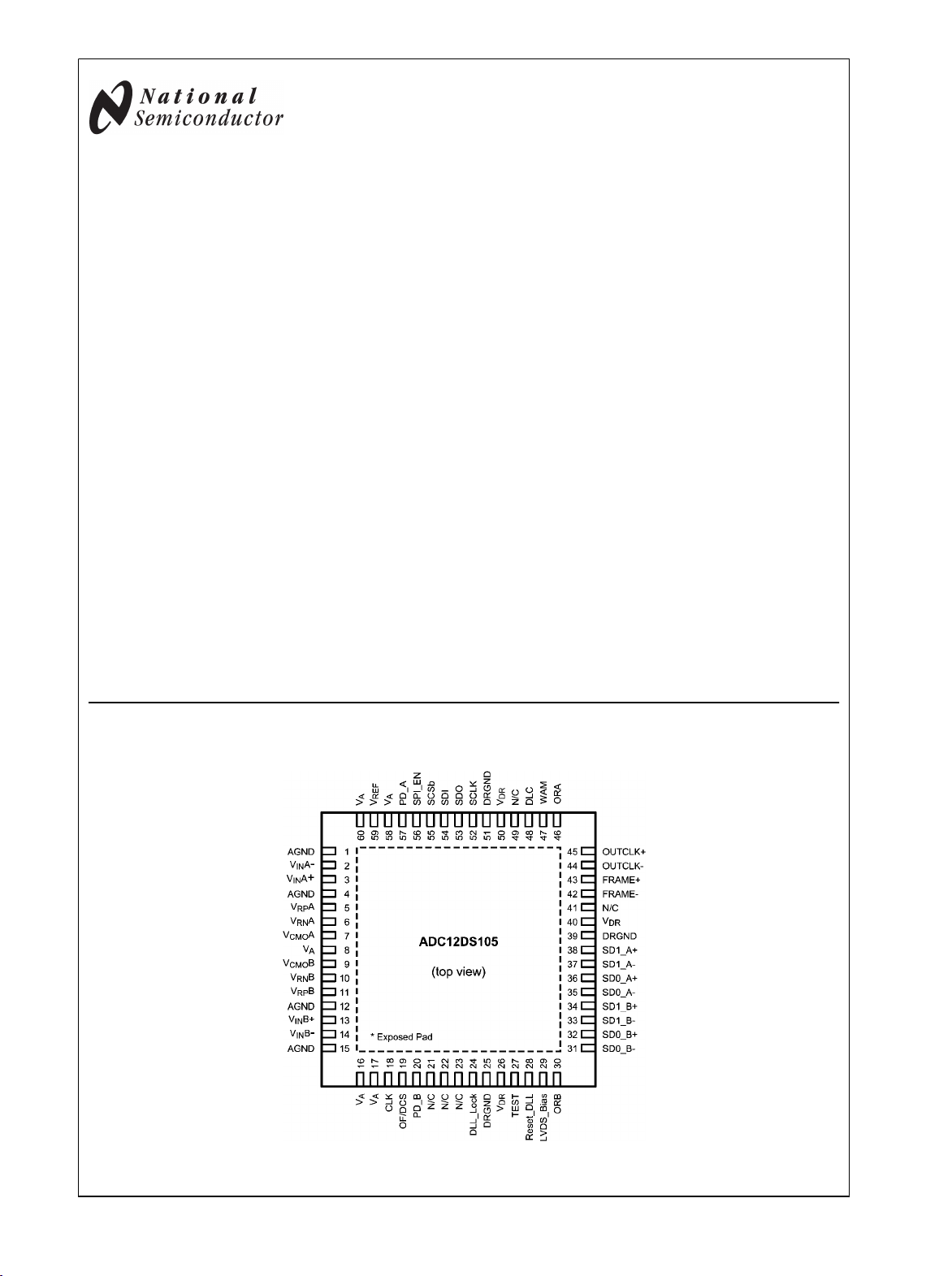
Connection Diagram
Features
Clock Duty Cycle Stabilizer
■
Single +3.0 or 3.3V supply operation
■
Serial LVDS Outputs
■
Serial Control Interface
■
Overrange outputs
■
60-pin LLP package, (9x9x0.8mm, 0.5mm pin-pitch)
■
Key Specifications
Resolution 12 Bits
■
Conversion Rate 105 MSPS
■
SNR (fIN = 240 MHz) 68.5 dBFS (typ)
■
SFDR (fIN = 240 MHz) 83 dBFS (typ)
■
Full Power Bandwidth 1 GHz (typ)
■
Power Consumption 1 W (typ)
■
Applications
High IF Sampling Receivers
■
Wireless Base Station Receivers
■
Test and Measurement Equipment
■
Communications Instrumentation
■
Portable Instrumentation
■
20211701
© 2008 National Semiconductor Corporation 202117 www.national.com
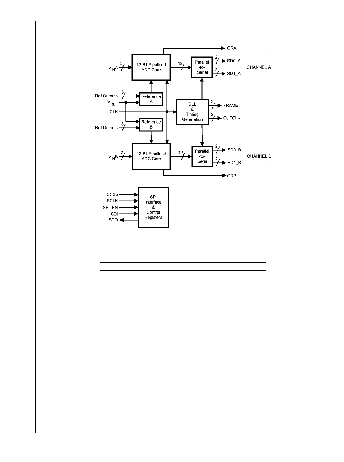
Block Diagram
ADC12DS105
Ordering Information
Industrial (−40°C ≤ TA ≤ +85°C)
20211702
Package
ADC12DS105CISQ 60 Pin LLP
ADC12DS105LFEB Evaluation Board for
Input Frequency < 70 MHz
www.national.com 2

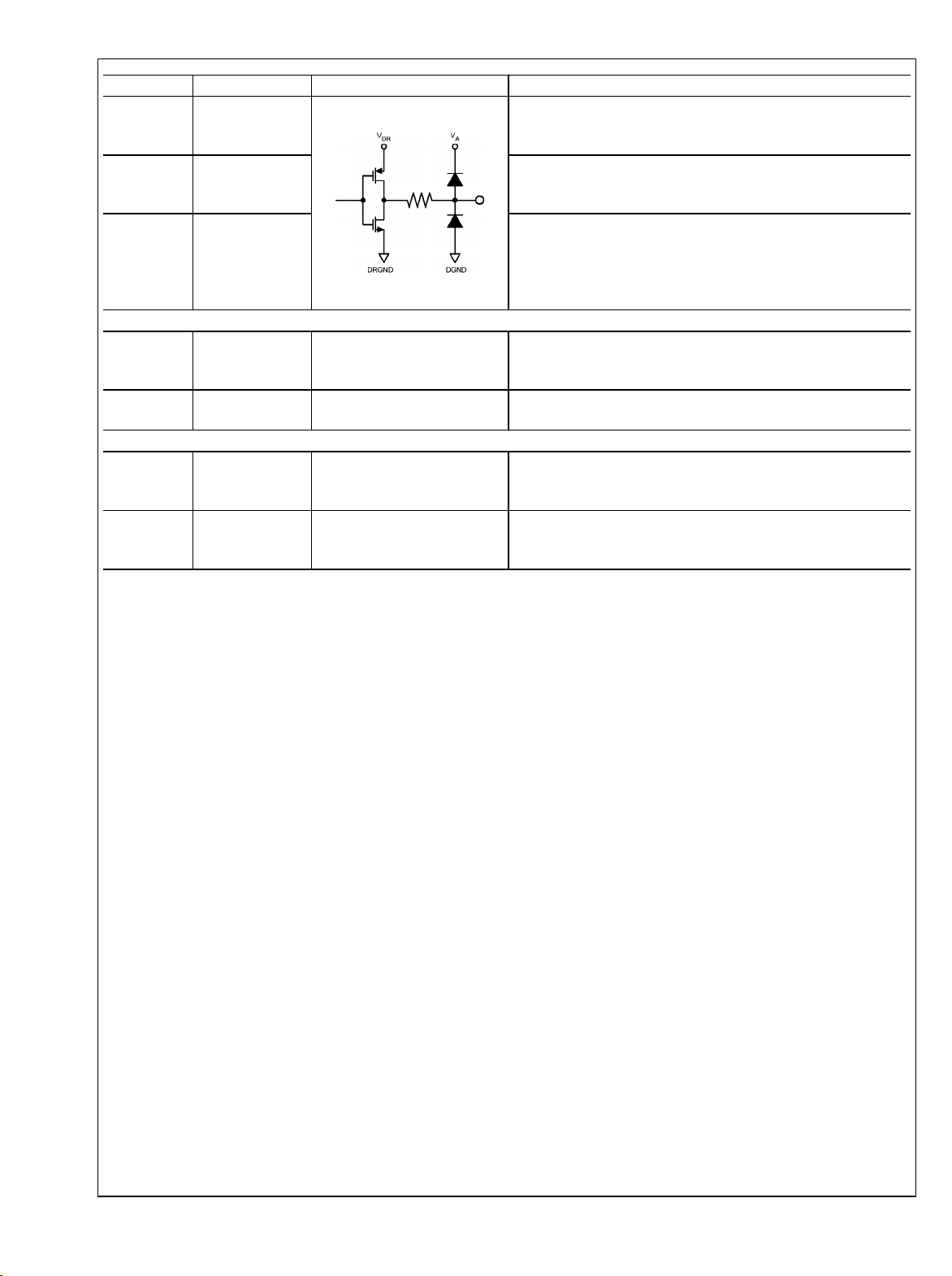
Pin Descriptions and Equivalent Circuits
Pin No. Symbol Equivalent Circuit Description
ANALOG I/O
3
13
2
14
VINA+
VINB+
VINAVINB-
Differential analog input pins. The differential full-scale input signal
level is 2V
with each input pin signal centered on a common
P-P
mode voltage, VCM.
ADC12DS105
5
11
7
9
6
10
59
29 LVDS_Bias
DIGITAL I/O
18 CLK
28 Reset_DLL
VRPA
VRPB
V
CMO
V
CMO
VRNA
VRNB
V
REF
These pins should each be bypassed to AGND with a low ESL
(equivalent series inductance) 0.1 µF capacitor placed very close
A
B
to the pin to minimize stray inductance. An 0201 size 0.1 µF
capacitor should be placed between VRP and VRN as close to the
pins as possible, and a 1 µF capacitor should be placed in parallel.
VRP and VRN should not be loaded. V
may be loaded to 1mA
CMO
for use as a temperature stable 1.5V reference.
It is recommended to use V
to provide the common mode
CMO
voltage, VCM, for the differential analog inputs.
Reference Voltage. This device provides an internally developed
1.2V reference. When using the internal reference, V
should be
REF
decoupled to AGND with a 0.1 µF and a 1µF, low equivalent series
inductance (ESL) capacitor.
This pin may be driven with an external 1.2V reference voltage.
This pin should not be used to source or sink current.
LVDS Driver Bias Resistor is applied from this pin to Analog
Ground. The nominal value is 3.6KΩ
The clock input pin.
The analog inputs are sampled on the rising edge of the clock input.
Reset_DLL input. This pin is normally low. If the input clock
frequency is changed abruptly, the internal timing circuits may
become unlocked. Cycle this pin high for 1 microsecond to re-lock
the DLL. The DLL will lock in several microseconds after
Reset_DLL is asserted.
19 OF/DCS
This is a four-state pin controlling the input clock mode and output
data format.
OF/DCS = VA, output data format is 2's complement without duty
cycle stabilization applied to the input clock
OF/DCS = AGND, output data format is offset binary, without duty
cycle stabilization applied to the input clock.
OF/DCS = (2/3)*VA, output data is 2's complement with duty cycle
stabilization applied to the input clock
OF/DCS = (1/3)*VA, output data is offset binary with duty cycle
stabilization applied to the input clock.
Note: This signal has no effect when SPI_EN is high and the SPI
interface is enabled.
3 www.national.com
Pin No. Symbol Equivalent Circuit Description
This is a two-state input controlling Power Down.
57
ADC12DS105
20
27 TEST
47 WAM
48 DLC
45
44
43
42
PD_A
PD_B
OUTCLK+
OUTCLK-
FRAME+
FRAME-
PD = VA, Power Down is enabled and power dissipation is reduced.
PD = AGND, Normal operation.
Note: This signal has no effect when SPI_EN is high and the SPI
interface is enabled.
Test Mode. When this signal is asserted high, a fixed test pattern
(101001100011 msb->lsb) is sourced at the data outputs.
With this signal deasserted low, the device is in normal operation
mode.
Note: This signal has no effect when SPI_EN is high and the SPI
interface is enabled.
Word Alignment Mode.
In single-lane mode this pin must be set to logic-0.
In dual-lane mode only, when this signal is at logic-0 the serial data
words are offset by half-word. With this signal at logic-1 the serial
data words are aligned with each other.
Note: This signal has no effect when SPI_EN is high and the SPI
interface is enabled.
Dual-Lane Configuration. The dual-lane mode is selected when
this signal is at logic-0. With this signal at logic-1, all data is sourced
on a single lane (SD1_x) for each channel.
Note: This signal has no effect when SPI_EN is high and the SPI
interface is enabled.
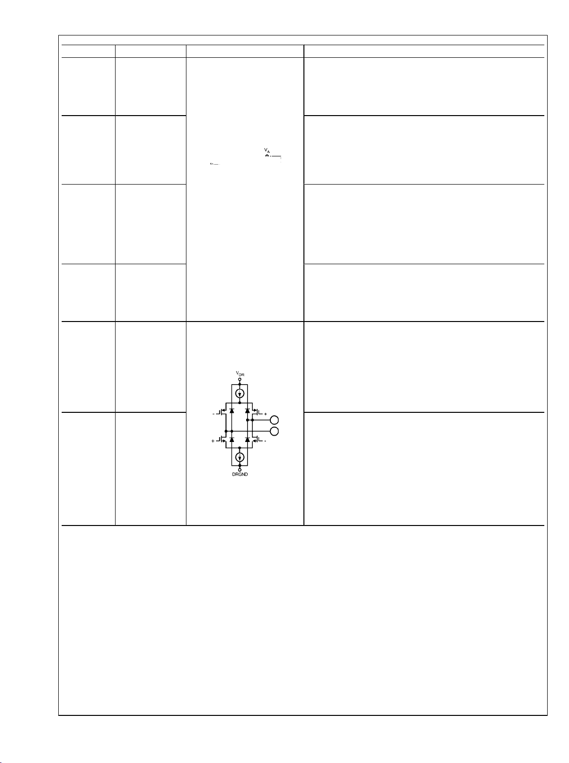
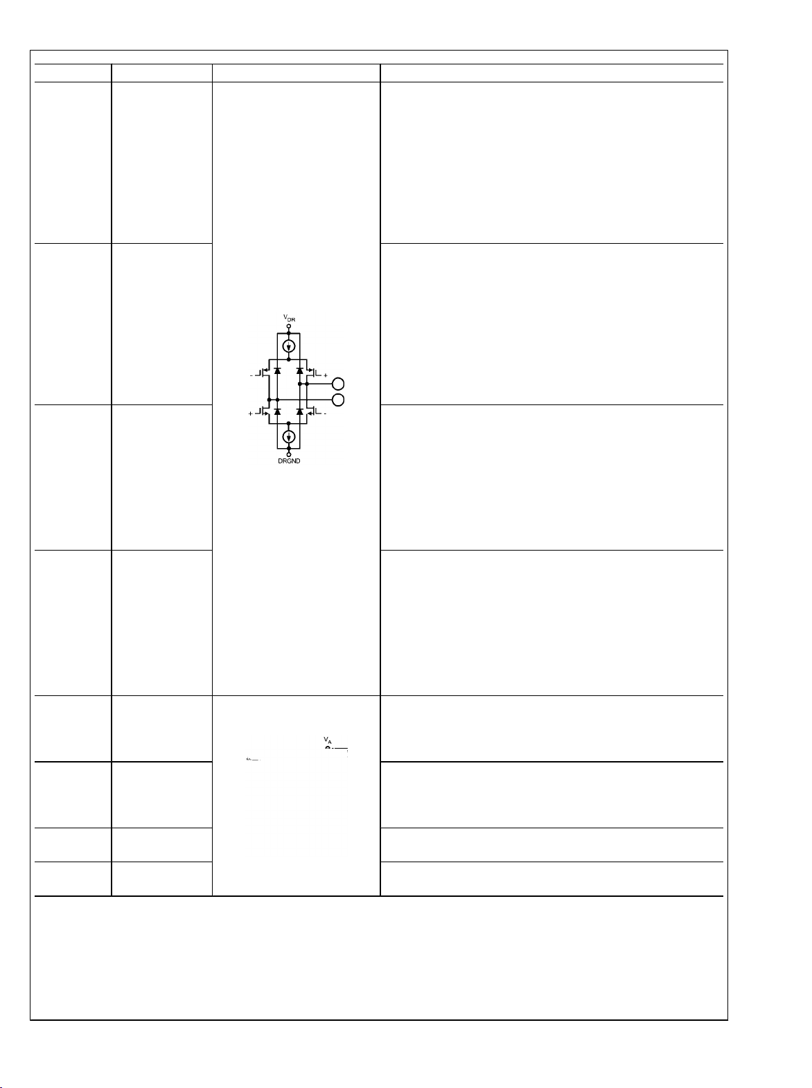
Serial Clock. This pair of differential LVDS signals provides the
serial clock that is synchronous with the Serial Data outputs. A bit
of serial data is provided on each of the active serial data outputs
with each falling and rising edge of this clock. This differential
output is always enabled while the device is powered up. In powerdown mode this output is held in logic-low state. A 100-ohm
termination resistor must always be used between this pair of
signals at the far end of the transmission line.
Serial Data Frame. This pair of differential LVDS signals transitions
at the serial data word boundaries. The SD1_A+/- and SD1_B+/output words always begin with the rising edge of the Frame signal.
The falling edge of the Frame signal defines the start of the serial
data word presented on the SD0_A+/- and SD0_B+/- signal pairs
in the Dual-Lane mode. This differential output is always enabled
while the device is powered up. In power-down mode this output is
held in logic-low state. A 100-ohm termination resistor must always
be used between this pair of signals at the far end of the
transmission line.
www.national.com 4
Pin No. Symbol Equivalent Circuit Description
Serial Data Output 1 for Channel A. This is a differential LVDS pair
of signals that carries channel A ADC’s output in serialized form.
The serial data is provided synchronous with the OUTCLK output.
In Single-Lane mode each sample’s output is provided in
38
37
34
33
36
35
32
31
56 SPI_EN
55 SCSb
52 SCLK
54 SDI
SD1_A+
SD1_A-
SD1_B+
SD1_B-
SD0_A+
SD0_A-
SD0_B+
SD0_B-
succession. In Dual-Lane mode every other sample output is
provided on this output. This differential output is always enabled
while the device is powered up. In power-down mode this output
holds the last logic state. A 100-ohm termination resistor must
always be used between this pair of signals at the far end of the
transmission line.
Serial Data Output 1 for Channel B. This is a differential LVDS pair
of signals that carries channel B ADC’s output in serialized form.
The serial data is provided synchronous with the OUTCLK output.
In Single-Lane mode each sample’s output is provided in
succession. In Dual-Lane mode every other sample output is
provided on this output. This differential output is always enabled
while the device is powered up. In power-down mode this output
holds the last logic state. A 100-ohm termination resistor must
always be used between this pair of signals at the far end of the
transmission line.
Serial Data Output 0 for Channel A. This is a differential LVDS pair
of signals that carries channel A ADC’s alternating samples’ output
in serialized form in Dual-Lane mode. The serial data is provided
synchronous with the OUTCLK output. In Single-Lane mode this
differential output is held in high impedance state. This differential
output is always enabled while the device is powered up. In power-
down mode this output holds the last logic state. A 100-ohm
termination resistor must always be used between this pair of
signals at the far end of the transmission line.
Serial Data Output 0 for Channel B. This is a differential LVDS pair
of signals that carries channel B ADC’s alternating samples’ output
in serialized form in Dual-Lane mode. The serial data is provided
synchronous with the OUTCLK output. In Single-Lane mode this
differential output is held in high impedance state. This differential
output is always enabled while the device is powered up. In power-
down mode this output holds the last logic state. A 100-ohm
termination resistor must always be used between this pair of
signals at the far end of the transmission line.
SPI Enable: The SPI interface is enabled when this signal is
asserted high. In this case the direct control pins have no effect.
When this signal is deasserted, the SPI interface is disabled and
the direct control pins are enabled.
Serial Chip Select: While this signal is asserted SCLK is used to
accept serial data present on the SDI input and to source serial
data on the SDO output. When this signal is deasserted, the SDI
input is ignored and the SDO output is in tri-state mode.
Serial Clock: Serial data are shifted into and out of the device
synchronous with this clock signal.
Serial Data-In: Serial data are shifted into the device on this pin
while SCSb signal is asserted.
ADC12DS105
5 www.national.com
Pin No. Symbol Equivalent Circuit Description
Serial Data-Out: Serial data are shifted out of the device on this pin
53 SDO
while SCSb signal is asserted. This output is in tri-state mode when
SCSb is deasserted.
ADC12DS105
46
30
ORA
ORB
Overrange. These CMOS outputs are asserted logic-high when
their respective channel’s data output is out-of-range in either high
or low direction.
DLL_Lock Output. When the internal DLL is locked to the input
CLK, this pin outputs a logic high. If the input CLK is changed
24 DLL_Lock
abruptly, the internal DLL may become unlocked and this pin will
output a logic low. Cycle Reset_DLL (pin 28) to re-lock the DLL to
the input CLK.
ANALOG POWER
8, 16, 17, 58,
60
1, 4, 12, 15,
Exposed Pad
V
A
AGND The ground return for the analog supply.
Positive analog supply pins. These pins should be connected to a
quiet source and be bypassed to AGND with 0.1 µF capacitors
located close to the power pins.
DIGITAL POWER
Positive driver supply pin for the output drivers. This pin should be
26, 40, 50
V
DR
connected to a quiet voltage source and be bypassed to DRGND
with a 0.1 µF capacitor located close to the power pin.
The ground return for the digital output driver supply. This pins
25, 39, 51 DRGND
should be connected to the system digital ground, but not be
connected in close proximity to the ADC's AGND pins.
www.national.com 6
ADC12DS105
Absolute Maximum Ratings (Notes 1, 3)
If Military/Aerospace specified devices are required,
please contact the National Semiconductor Sales Office/
Distributors for availability and specifications.
Supply Voltage (VA, VDR) −0.3V to 4.2V
Voltage on Any Pin
(Not to exceed 4.2V)
Input Current at Any Pin other
than Supply Pins (Note 4)
−0.3V to (VA +0.3V)
±5 mA
Operating Ratings (Notes 1, 3)
Operating Temperature
Supply Voltage (VA=VDR) +2.7V to +3.6V
Clock Duty Cycle
(DCS Enabled) 30/70 %
(DCS disabled) 45/55 %
V
CM
|AGND-DRGND|
−40°C ≤ TA ≤ +85°C
1.4V to 1.6V
≤100mV
Package Input Current (Note 4) ±50 mA
Max Junction Temp (TJ) +150°C
Thermal Resistance (θJA)
30°C/W
ESD Rating
Human Body Model (Note 6) 2500V
Machine Model (Note 6) 250V
Storage Temperature −65°C to +150°C
Soldering process must comply with National
Semiconductor's Reflow Temperature Profile
specifications. Refer to www.national.com/packaging.
(Note 7)
Converter Electrical Characteristics
Unless otherwise specified, the following specifications apply: AGND = DRGND = 0V, VA = +3.3V, VDR = +3.0V, Internal V
+1.2V, f
T
MAX
Symbol Parameter Conditions
= 105 MHz, VCM = V
CLK
, CL = 5 pF/pin. Typical values are for TA = 25°C. Boldface limits apply for T
CMO
. All other limits apply for TA = 25°C (Notes 8, 9)
Typical
(Note 10)
MIN
Limits
STATIC CONVERTER CHARACTERISTICS
Resolution with No Missing Codes 12 Bits (min)
INL Integral Non Linearity
DNL Differential Non Linearity
±0.5
±0.3
2 LSB (max)
-2 LSB (min)
0.8 LSB (max)
-0.8 LSB (min)
PGE Positive Gain Error 0.15 ±1 %FS (max)
NGE Negative Gain Error 0.07 ±1 %FS (max)
TC PGE Positive Gain Error Tempco
TC NGE Negative Gain Error Tempco
V
OFF
TC V
Offset Error
Offset ErrorTempco
OFF
−40°C ≤ TA ≤ +85°C
−40°C ≤ TA ≤ +85°C
−40°C ≤ TA ≤ +85°C
ppm/°C
ppm/°C
0.03 ±0.55 %FS (max)
ppm/°C
Under Range Output Code 0 0
Over Range Output Code 4095 4095
REFERENCE AND ANALOG INPUT CHARACTERISTICS
V
CMO
V
CM
C
IN
V
REF
TC V
V
RP
V
RN
Common Mode Output Voltage 1.5
Analog Input Common Mode Voltage 1.5
VIN Input Capacitance (each pin to GND)
(Note 11)
VIN = 1.5 Vdc
± 0.5 V
(CLK LOW) 8.5 pF
(CLK HIGH) 3.5 pF
Internal Reference Voltage 1.18
Internal Reference Voltage Tempco
REF
−40°C ≤ TA ≤ +85°C
18 ppm/°C
Internal Reference Top 2.0 V
Internal Reference Bottom 1.0 V
1.4
1.6
1.4
1.6
1.17
1.21
REF
≤ TA ≤
Units
(Limits)
V (min)
V (max)
V (min)
V (max)
V (min)
V (max)
=
7 www.national.com
Symbol Parameter Conditions
Internal Reference Accuracy
ADC12DS105
EXT
V
REF
External Reference Voltage 1.2
(VRP-VRN)
Typical
(Note 10)
0.97
Limits
0.89
1.06
1.176
1.224
Dynamic Converter Electrical Characteristics
Unless otherwise specified, the following specifications apply: AGND = DRGND = 0V, VA = +3.3V, VDR = +3.0V, Internal V
+1.2V, f
T
MAX
Symbol Parameter Conditions
DYNAMIC CONVERTER CHARACTERISTICS, AIN = -1dBFS
FPBW Full Power Bandwidth -1 dBFS Input, −3 dB Corner 1.0 GHz
SNR Signal-to-Noise Ratio
SFDR Spurious Free Dynamic Range
ENOB Effective Number of Bits
THD Total Harmonic Disortion
H2 Second Harmonic Distortion
H3 Third Harmonic Distortion
SINAD Signal-to-Noise and Distortion Ratio
IMD Intermodulation Distortion
= 105 MHz, VCM = V
CLK
, CL = 5 pF/pin, . Typical values are for TA = 25°C. Boldface limits apply for T
CMO
. All other limits apply for TA = 25°C (Notes 8, 9)
fIN = 10 MHz
fIN = 70 MHz
fIN = 240 MHz
fIN = 10 MHz
fIN = 70 MHz
fIN = 240 MHz
fIN = 10 MHz
fIN = 70 MHz
fIN = 240 MHz
fIN = 10 MHz
fIN = 70 MHz
fIN = 240 MHz
fIN = 10 MHz
fIN = 70 MHz
fIN = 240 MHz
fIN = 10 MHz
fIN = 70 MHz
fIN = 240 MHz
fIN = 10 MHz
fIN = 70 MHz
fIN = 240 MHz
fIN = 19.5 and 20.5 MHz,
each -7dBFS
Typical
(Note 10)
Limits
71 dBFS
70 dBFS
68.5 67.4 dBFS
88 dBFS
85 dBFS
83 76.5 dBFS
11.5 Bits
11.3 Bits
11 10.7 Bits
−86 dBFS
−85 dBFS
−80 -74 dBFS
−90 dBFS
−88 dBFS
−83 -76.5 dBFS
−88 dBFS
−85 dBFS
−83 -76.5 dBFS
70.8 dBFS
69.9 dBFS
68.2 66.5 dBFS
-82 dBFS
(Limits)
V (min)
V (max)
V (min)
V (max)
≤ TA ≤
MIN
(Limits)
(Note 2)
Units
REF
Units
=
Logic and Power Supply Electrical Characteristics
Unless otherwise specified, the following specifications apply: AGND = DRGND = 0V, VA = +3.3V, VDR = +3.0V, Internal V
+1.2V, f
T
MAX
Symbol Parameter Conditions
DIGITAL INPUT CHARACTERISTICS (CLK, PD_A,PD_B,SCSb,SPI_EN,SCLK,SDI,TEST,WAM,DLC)
V
IN(1)
V
IN(0)
I
IN(1)
I
IN(0)
www.national.com 8
= 105 MHz, VCM = V
CLK
, CL = 5 pF/pin. Typical values are for TA = 25°C. Boldface limits apply for T
CMO
. All other limits apply for TA = 25°C (Notes 8, 9)
Logical “1” Input Voltage
Logical “0” Input Voltage
Logical “1” Input Current
VD = 3.6V
VD = 3.0V
VIN = 3.3V
Logical “0” Input Current VIN = 0V
Typical
(Note 10)
Limits
2.0 V (min)
0.8 V (max)
10
µA
−10 µA
MIN
REF
≤ TA ≤
Units
(Limits)
=
 Loading...