

ADC122S021
2 Channel, 200 KSPS 12-Bit A/D Converter
ADC122S021 2 Channel, 200 KSPS 12-Bit A/D Converter
April 2005
General Description
The ADC122S021 is a low-power, two-channel CMOS 12-bit
analog-to-digital converter with a high-speed serial interface.
Unlike the conventional practice of specifying performance
at a single sample rate only, the ADC122S021 is fully specified over a sample rate range of 50 kSPS to 200 kSPS. The
converter is based on a successive-approximation register
architecture with an internal track-and-hold circuit. It can be
configured to accept one or two input signals at inputs IN1
and IN2.
The output serial data is straight binary, and is compatible
with several standards, such as SPI
IRE, and many common DSP serial interfaces.
The ADC122S021 operates with a single supply that can
range from +2.7V to +5.25V. Normal power consumption
using a +3V or +5V supply is 2.2 mW and 7.9 mW, respectively. The power-down feature reduces the power consumption to just 0.14 µW using a +3V supply, or 0.32 µW using a
+5V supply.
The ADC122S021 is packaged in an 8-lead MSOP package.
Operation over the industrial temperature range of −40˚C to
+85˚C is guaranteed.
™
, QSPI™, MICROW-
Features
n Specified over a range of sample rates.
n Two input channels
n Variable power management
n Single power supply with 2.7V - 5.25V range
Key Specifications
n DNL +0.4 / −0.2 LSB (typ)
n INL
n SNR 72.0 dB (typ)
n Power Consumption
— 3V Supply 2.2 mW (typ)
— 5V Supply 7.9 mW (typ)
Applications
n Portable Systems
n Remote Data Acquisition
n Instrumentation and Control Systems
Pin-Compatible Alternatives by Resolution and Speed
All devices are fully pin and function compatible.
Resolution Specified for Sample Rate Range of:
50 to 200 kSPS 200 to 500 kSPS 500 kSPS to 1 MSPS
12-bit ADC122S021 ADC122S051 ADC122S101
10-bit ADC102S021 ADC102S051 ADC102S101
8-bit ADC082S021 ADC082S051 ADC082S101
±
0.35 LSB (typ)
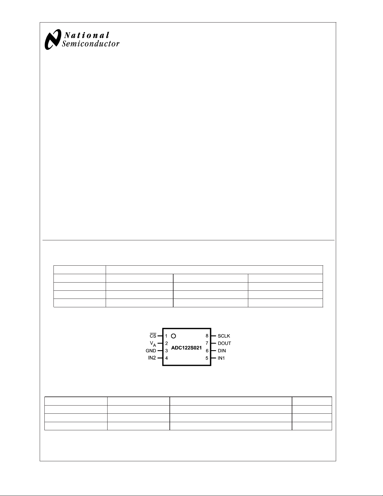
Connection Diagram
20124605
Ordering Information
Order Code Temperature Range Description Top Mark
ADC122S021CIMM −40˚C to +85˚C 8-Lead MSOP Package X18C
ADC122S021CIMMX −40˚C to +85˚C 8-Lead MSOP Package, Tape & Reel X18C
ADC122S021EVAL Evaluation Board
TRI-STATE®is a trademark of National Semiconductor Corporation
™
QSPI
and SPI™are trademarks of Motorola, Inc.
© 2005 National Semiconductor Corporation DS201246 www.national.com
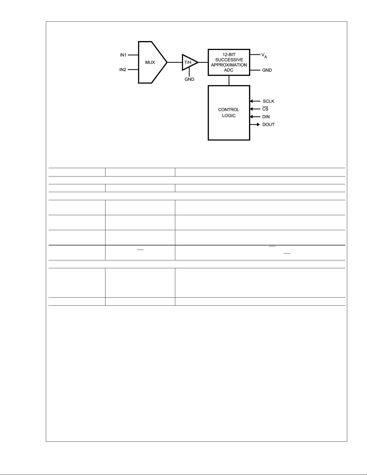
Block Diagram
ADC122S021
Pin Descriptions and Equivalent Circuits
Pin No. Symbol Description
ANALOG I/O
5,4 IN1 and IN2 Analog inputs. These signals can range from 0V to V
DIGITAL I/O
8 SCLK
7 DOUT
6 DIN
1CS
POWER SUPPLY
2V
3 GND The ground return for the analog supply and signals.
A
20124607
.
A
Digital clock input. This clock directly controls the conversion
and readout processes.
Digital data output. The output samples are clocked out of this
pin on falling edges of the SCLK pin.
Digital data input. The ADC122S021’s Control Register is
loaded through this pin on rising edges of the SCLK pin.
Chip select. On the falling edge of CS, a conversion process
begins. Conversions continue as long as CS is held low.
Positive supply pin. This pin should be connected to a quiet
+2.7V to +5.25V source and bypassed to GND witha1µF
capacitor and a 0.1 µF monolithic capacitor located within 1
cm of the power pin.
www.national.com 2
ADC122S021
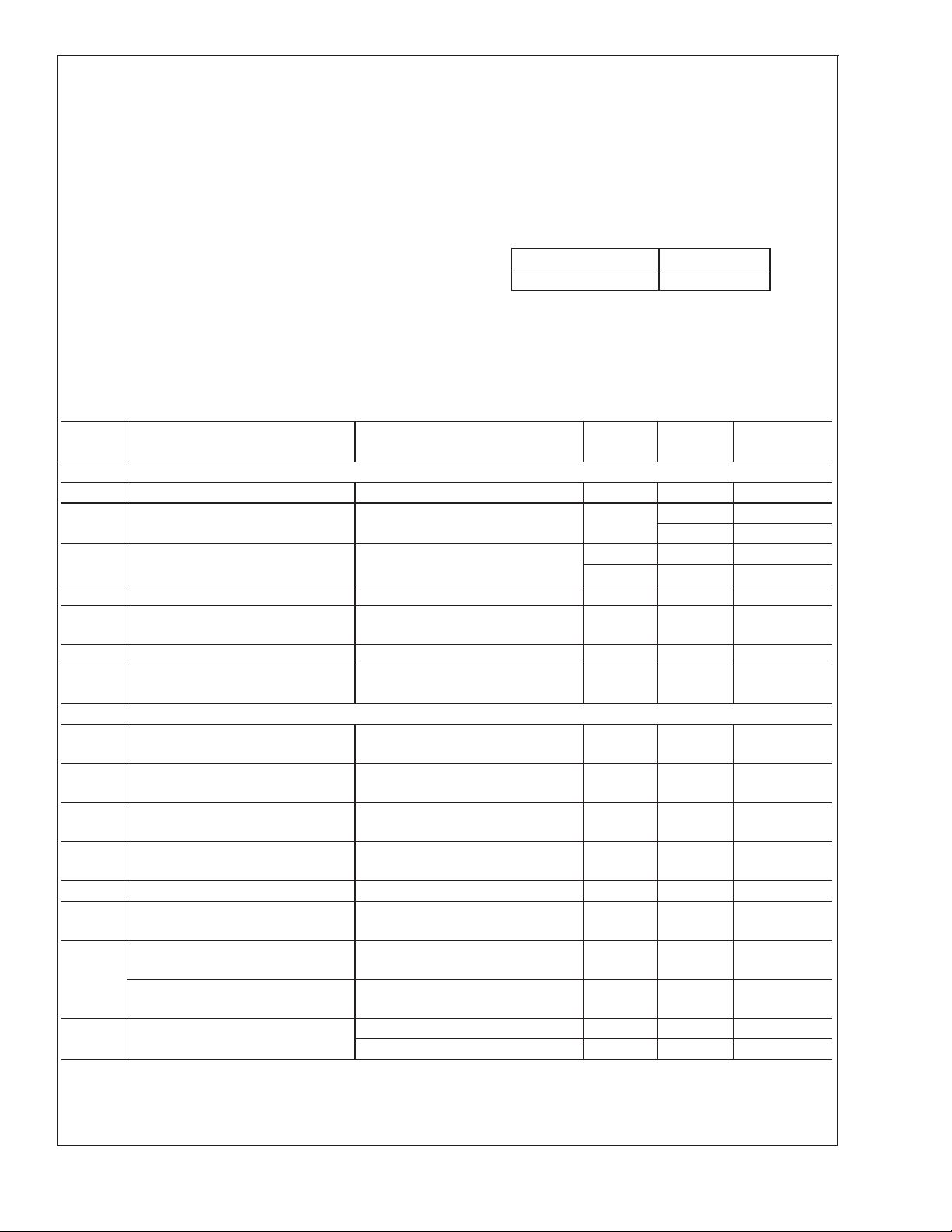
Absolute Maximum Ratings (Notes 1, 2)
If Military/Aerospace specified devices are required,
please contact the National Semiconductor Sales Office/
Distributors for availability and specifications.
Analog Supply Voltage V
A
Voltage on Any Pin to GND −0.3V to V
Input Current at Any Pin (Note 3)
Package Input Current (Note 3)
Power Consumption at T
= 25˚C See (Note 4)
A
ESD Susceptibility (Note 5)
Human Body Model
Machine Model
Junction Temperature +150˚C
Storage Temperature −65˚C to +150˚C
−0.3V to 6.5V
+0.3V
A
±
10 mA
±
20 mA
2500V
250V
Operating Ratings (Notes 1, 2)
Operating Temperature Range −40˚C ≤ T
V
Supply Voltage +2.7V to +5.25V
A
Digital Input Pins Voltage Range −0.3V to V
Clock Frequency 0.8 MHz to 3.2 MHz
Analog Input Voltage 0V to V
Package Thermal Resistance
Package θ
8-lead MSOP 250˚C / W
Soldering process must comply with National Semiconductor’s Reflow Temperature Profile specifications. Refer to
www.national.com/packaging. (Note 6)
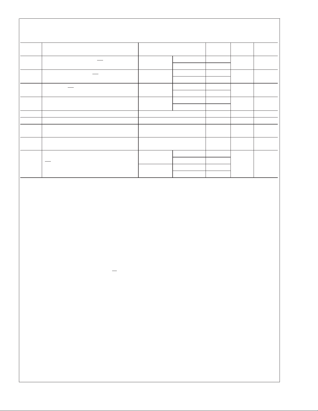
ADC122S021 Converter Electrical Characteristics (Note 9)
The following specifications apply for VA= +2.7V to 5.25V, GND = 0V, f
kSPS, C
= 35 pF unless otherwise noted. Boldface limits apply for TA=T
L
Symbol Parameter Conditions Typical
STATIC CONVERTER CHARACTERISTICS
Resolution with No Missing Codes 12 Bits
INL Integral Non-Linearity
DNL Differential Non-Linearity
V
OFF
OEM
Offset Error +0.37
Channel to Channel Offset Error
Match
FSE Full Scale Error
FSEM
Channel to Channel Full-Scale Error
Match
DYNAMIC CONVERTER CHARACTERISTICS
V
= +2.7 to 5.25V,
SINAD Signal-to-Noise Plus Distortion Ratio
SNR Signal-to-Noise Ratio
THD Total Harmonic Distortion
SFDR Spurious-Free Dynamic Range
ENOB Effective Number of Bits V
Channel-to-Channel Crosstalk
Intermodulation Distortion, Second
IMD
Order Terms
Intermodulation Distortion, Third
Order Terms
FPBW -3 dB Full Power Bandwidth
A
= 39.9 kHz, −0.02 dBFS
f
IN
V
= +2.7 to 5.25V,
A
= 39.9 kHz, −0.02 dBFS
f
IN
V
= +2.7 to 5.25V,
A
= 39.9 kHz, −0.02 dBFS
f
IN
V
= +2.7 to 5.25V,
A
= 39.9 kHz, −0.02 dBFS
f
IN
= +2.7 to 5.25V, 11.7 11.2 Bits (min)
A
V
= +5.25V
A
= 39.9 kHz
f
IN
V
= +5.25V,
A
= 40.161 kHz, fb= 41.015 kHz
f
a
V
= +5.25V,
A
= 40.161 kHz, fb= 41.015 kHz
f
a
V
= +5V 11 MHz
A
V
= +3V 8 MHz
A
= 0.8 MHz to 3.2 MHz, f
SCLK
MIN
to T
MAX
: all other limits TA= 25˚C.
±
0.35
+0.4 +1.1 LSB (max)
−0.2 −0.8 LSB (min)
±
0.1
±
0.52
+0.1
72 69.2 dB (min)
72 70.6 dB (min)
−84 −75 dB (max)
86 76 dB (min)
−86 dB
−81 dB
−88 dB
≤ +85˚C
A
JA
= 50 kSPS to 200
SAMPLE
Limits
(Note 7)
Units
+0.8 LSB (max)
−1.1 LSB (min)
±
1.3 LSB (max)
±
1.0 LSB (max)
±
1.5 LSB (max)
±
1.0 LSB (max)
A
A
www.national.com3
ADC122S021 Converter Electrical Characteristics (Note 9) (Continued)
The following specifications apply for VA= +2.7V to 5.25V, GND = 0V, f
kSPS, C
Symbol Parameter Conditions Typical
ADC122S021
= 35 pF unless otherwise noted. Boldface limits apply for TA=T
L
ANALOG INPUT CHARACTERISTICS
V
I
C
IN
DCL
INA
Input Range 0 to V
DC Leakage Current
Input Capacitance
Track Mode 33 pF
Hold Mode 3 pF
DIGITAL INPUT CHARACTERISTICS
= +5.25V 2.4 V (min)
V
V
IH
V
IL
I
IN
C
IND
Input High Voltage
Input Low Voltage 0.8 V (max)
Input Current VIN=0VorVIN=V
Digital Input Capacitance 2 4 pF (max)
A
V
= +3.6V 2.1 V (min)
A
A
DIGITAL OUTPUT CHARACTERISTICS
V
V
I
I
C
OZH
OZL
OH
OL
OUT
I
Output High Voltage
Output Low Voltage
,
TRI-STATE®Leakage Current
SOURCE
I
SOURCE
I
SINK
I
SOURCE
TRI-STATE®Output Capacitance 2 4 pF (max)
= 200 µA VA− 0.03 VA− 0.5 V (min)
=1mA VA− 0.1
= 200 µA 0.02 0.4 V (max)
= 1 mA 0.1 V
Output Coding Straight (Natural) Binary
POWER SUPPLY CHARACTERISTICS (C
V
A
Analog Supply Voltage
=10pF)
L
VA= +5.25V,
Supply Current, Normal Mode
(Operational, CS low)
I
A
Supply Current, Shutdown (CS high)
f
V
f
VA= +5.25V,
f
V
f
Power Consumption, Normal Mode
P
D
(Operational, CS low)
Power Consumption, Shutdown (CS
high)
VA= +5.25V 7.9 11 mW (max)
V
V
V
= 200 KSPS, fIN= 39.9 kHz
SAMPLE
= +3.6V,
A
= 200 KSPS, fIN= 39.9 kHz
SAMPLE
= 0 kSPS
SAMPLE
= +3.6V,
A
= 0 kSPS
SAMPLE
= +3.6V 2.2 3.6 mW (max)
A
= +5.25V 0.32 µW
A
= +3.6V 0.14 µW
A
AC ELECTRICAL CHARACTERISTICS
f
SCLK
f
S
t
CONV
DC SCLK Duty Cycle f
t
ACQ
Maximum Clock Frequency (Note 8)
Sample Rate (Note 8)
Conversion Time 13 SCLK cycles
= 3.2 MHz 50
SCLK
Track/Hold Acquisition Time Full-Scale Step Input 3 SCLK cycles
Throughput Time Acquisition Time + Conversion Time 16 SCLK cycles
= 0.8 MHz to 3.2 MHz, f
SCLK
MIN
to T
MAX
: all other limits TA= 25˚C.
±
±
±
1.5 2.1 mA (max)
0.62 1.0 mA (max)
= 50 kSPS to 200
SAMPLE
0.02
0.02
0.01
Limits
(Note 7)
A
±
1 µA (max)
±
10 µA (max)
±
1 µA (max)
Units
2.7 V (min)
5.25 V (max)
60 nA
38 nA
0.8 MHz (min)
3.2 MHz (max)
50 kSPS (min)
200 kSPS (max)
30 % (min)
70 % (max)
V
www.national.com 4
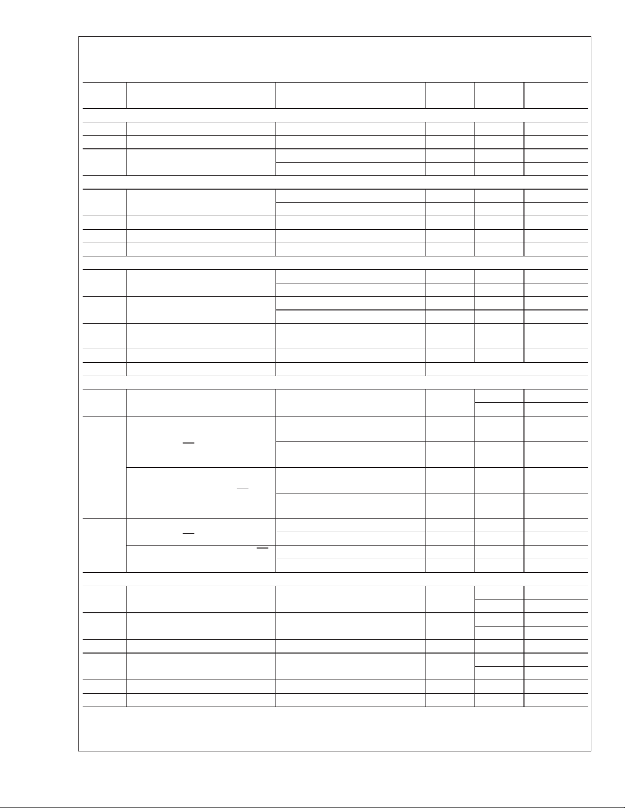
ADC122S021 Timing Specifications
The following specifications apply for VA= +2.7V to 5.25V, GND = 0V, f
kSPS, C
=35pF,Boldface limits apply for TA=T
L
MIN
to T
: all other limits TA= 25˚C.
MAX
Symbol Parameter Conditions Typical
t
t
t
CSU
CLH
t
EN
ACC
t
SU
t
t
CH
t
CL
Setup Time SCLK High to CS Falling Edge (Note 10)
Hold time SCLK Low to CS Falling Edge (Note 10)
Delay from CS Until DOUT active
Data Access Time after SCLK Falling Edge
Data Setup Time Prior to SCLK Rising Edge +3 10 ns (min)
Data Valid SCLK Hold Time +3 10 ns (min)
H
SCLK High Pulse Width
SCLK Low Pulse Width
Output Falling
t
DIS
CS Rising Edge to DOUT High-Impedance
Output Rising
Note 1: Absolute Maximum Ratings indicate limits beyond which damage to the device may occur. Operating Ratings indicate conditions for which the device is
functional, but do not guarantee specific performance limits. For guaranteed specifications and test conditions, see the Electrical Characteristics. The guaranteed
specifications apply only for the test conditions listed. Some performance characteristics may degrade when the device is not operated under the listed test
conditions.
Note 2: All voltages are measured with respect to GND = 0V, unless otherwise specified.
Note 3: When the input voltage at any pin exceeds the power supply (that is, V
mA maximum package input current rating limits the number of pins that can safely exceed the power supplies with an input current of 10 mA to two. The Absolute
Maximum Rating specification does not apply to the V
Note 4: The absolute maximum junction temperature (T
junction-to-ambient thermal resistance (θ
for maximum power dissipation listed above will be reached only when the device is operated in a severe fault condition (e.g. when input or output pins are driven
beyond the power supply voltages, or the power supply polarity is reversed). Obviously, such conditions should always be avoided.
Note 5: Human body model is 100 pF capacitor discharged through a 1.5 kΩ resistor. Machine model is 220 pF discharged through zero ohms.
Note 6: Reflow temperature profiles are different for lead-free and non-lead-free packages.
Note 7: Tested limits are guaranteed to National’s AOQL (Average Outgoing Quality Level).
Note 8: This is the frequency range over which the electrical performance is guaranteed. The device is functional over a wider range which is specified under
Operating Ratings.
Note 9: Data sheet min/max specification limits are guaranteed by design, test, or statistical analysis.
Note 10: Clock may be in any state (high or low) when CS is asserted, with the restrictions on setup and hold time given by t
), and the ambient temperature (TA), and can be calculated using the formula PDMAX=(TJmax − TA)/θJA. The values
JA
pin. The current into the VApin is limited by the Analog Supply Voltage specification.
A
max) for this device is 150˚C. The maximum allowable power dissipation is dictated by TJmax, the
J
IN
<
GND or V
= 0.8 MHz to 3.2 MHz, f
SCLK
= 50 kSPS to 200
SAMPLE
Limits
(Note 7)
= +3.0V −3.5
V
A
V
= +5.0V −0.5
A
= +3.0V +4.5
V
A
V
= +5.0V +1.5
A
VA= +3.0V +4
V
= +5.0V +2
A
= +3.0V +14.5
V
A
V
= +5.0V +13
A
0.5 x
t
SCLK
0.5 x
t
SCLK
= +3.0V 1.8
V
A
V
= +5.0V 1.3
A
V
= +3.0V 1.0
A
V
= +5.0V 1.0
A
>
VA), the current at that pin should be limited to 10 mA. The 20
IN
CSU
10 ns (min)
10 ns (min)
30 ns (max)
30 ns (max)
0.3 x
t
SCLK
0.3 x
t
SCLK
20 ns (max)
and t
.
CLH
Units
ns (min)
ns (min)
ADC122S021
www.national.com5
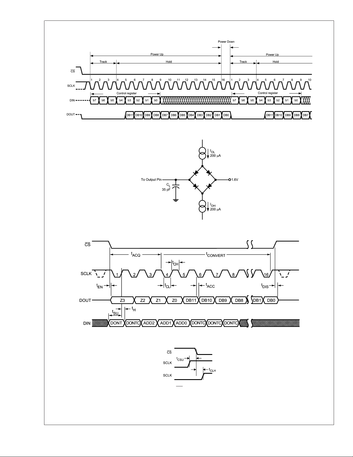
Timing Diagrams
ADC122S021
ADC122S021 Operational Timing Diagram
20124608
Timing Test Circuit
20124651
ADC122S021 Serial Timing Diagram
SCLK and CS Timing Parameters
www.national.com 6
20124606
20124650
 Loading...