

MXIC MX23C4100 Datasheet

FEATURES
MX23C4100
4M-BIT [512K x 8/256K x 16] MASK ROM
• Switchable organization
- 512K x 8 (byte mode)
- 256K x 16 (word mode)
• Single +5V power supply
• Fast access time:100/120/150ns
GENERAL DESCRIPTION
The MX23C4100 is a 5V only, 4M-bit, Read Only
Memory . It is organized as 512Kx8 bits (byte mode) or
as 256Kx16 bit (word mode) depending on BYTE (pin
31) voltage level. MX23C4100 has a static standby
mode, and has an access time of 100/120/150/200ns.
It is designed to be compatible with all microprocessors
and similar applications in which high performance, large
bit storage and simple interfacing are important design
considerations.
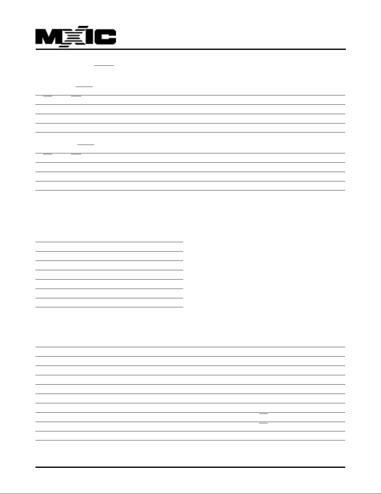
PIN CONFIGURATION
40 PDIP/SOP
A17
CE
VSS
OE
Q0
Q8
Q1
Q9
Q2
Q10
Q3
Q11
1
A7
2
A6
3
A5
4
A4
5
A3
6
A2
7
A1
8
A0
9
10
11
12
MX23C4100
13
14
15
16
17
18
19
20
A8
40
A9
39
A10
38
A11
37
A12
36
A13
35
A14
34
A15
33
A16
32
BYTE
31
VSS
30
Q15/A-1
29
Q7
28
Q14
27
Q6
26
Q13
25
Q5
24
Q12
23
Q4
22
VCC
21
• Totally static operation
• Completely TTL compatible
• Operating current: 60mA
• Standby current: 100uA
• Package
- 40 pin DIP (600 mil)
- 40 pin SOP
MX23C4100 offers automatic pow er-down, with powerdown controlled by the chip enable (CE) input. When
CE is not selected, the device automatically powers
down and remains in a low-power standb y mode as long
as CE stays in the unselected mode.
The OE input as well as OE input may be programmed
active Low.
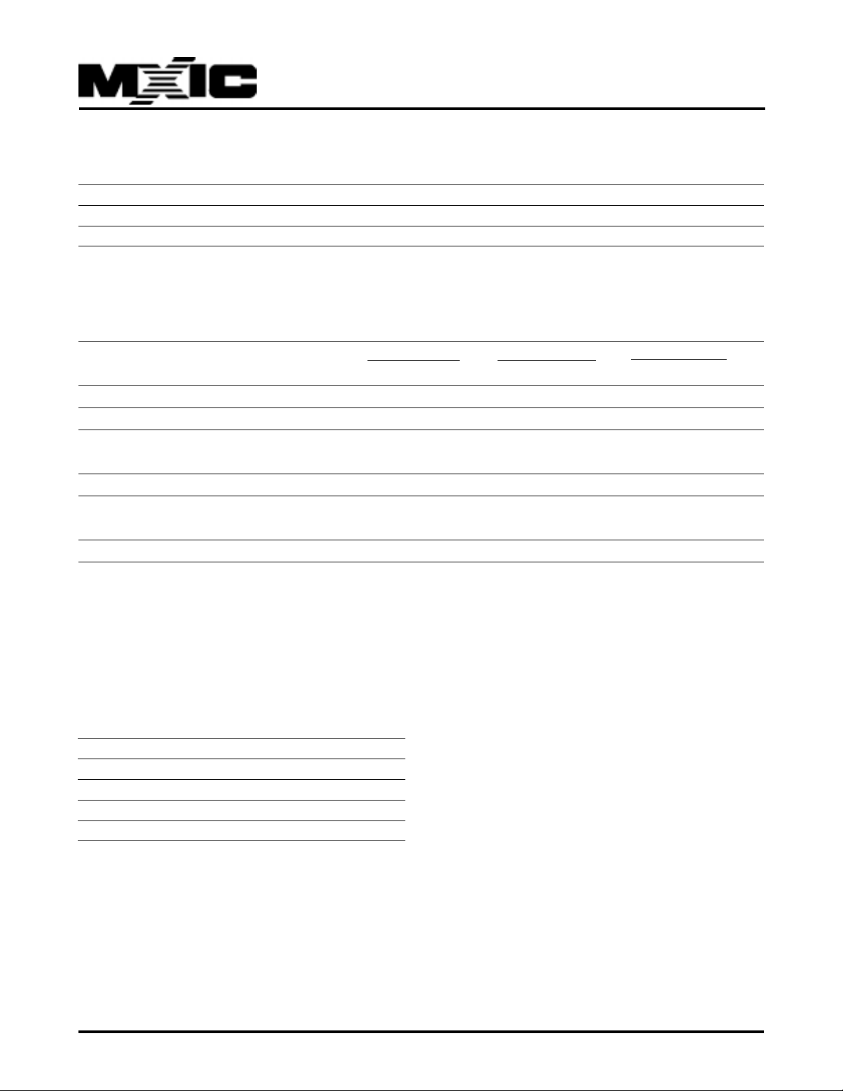
BLOCK DIAGRAM
CE
OE
BYTE
Q15/A-1
A0~A17
ADDRESS
INPUTS
VCC
VSS
.
.
.
.
.
.
.
.
CONTROL
LOGIC
Y-DECODER
X-DECODER
.
.
.
.
.
.
.
.
OUTPUT
BUFFERS
Y-DECODER
4M BIT
ROM ARRAY
Q0~Q14
PIN DESCRIPTION
Symbol Pin Function
A0~A17 Address Input
Q0~Q14 Data Output
CE Chip Enable Input
OE Output Enab le Input
BYTE Word/Byte Selection
Q15/A-1 Q15(Word mode)/LSB address(Byte
mode)
VCC Po wer Supply Pin (+5V)
VSS Ground Pin
P/N:PM0136 REV. 3.6, JUL. 16, 2001
1
MX23C4100
TRUTH TABLE OF BYTE FUNCTION
BYTE MODE (BYTE=VSS)
CE OE D15/A-1 MODE D0-D7 SUPPL Y CURRENT NO TE
H X X Non selected High Z Standby (ICC2) 1
L H X Non selected High Z Operating (ICC1) 1
L L A-1 input Selected DOUT Operating (ICC1) 1
WORD MODE (BYTE=VCC)
CE OE D15/A-1 MODE D0-D7 SUPPL Y CURRENT NO TE
H X High Z Non selected High Z Standby (ICC2) 1
L H High Z Non selected High Z Operating (ICC1) 1
L L DOUT Selected DOUT Operating (ICC1) 1
NOTE1:X=H or L
ABSOLUTE MAXIMUM RATINGS*
RATING VALUE
Ambient Operating Temperature 0°C to 70°C
Storage T emperature -65°C to 125°C
Applied Input Voltage -0.5V to 7.0V
Applied Output Voltage -0.5V to 7.0V
VCC to Ground Potential -0.5V to 7.0V
Power Dissipation 1.0W
*Note:
Stress greater than those listed under ABSOLUTE MAXIMUM
RA TINGS ma y cause permanent damage to the device. This
is a stress rating only and functional operation of the device
at these or any other conditions above those indicated in the
operational sections of this specification is not implied. Exposure to absolute maximum rating conditions for extended
period may affect reliability.
DC CHARACTERISTICS (Ta = 0°C ~ 70°C, VCC = 5V±10%)
Item Symbol MIN. MAX. Conditions
Output High Voltage VOH 2.4V - IOH = -1.0mA
Output Low Voltage VOL - 0.4V IOL = 2.1mA
Input High Voltage VIH 2.2V VCC+0.3V
Input Low Voltage VIL -0.3V 0.8V
Input Leakage Current ILI - 10uA VIN=0 to 5.5V
Output Leakage Current ILO - 10uA VOUT=0 to 5.5V
Power-Do wn Supply Current ICC3 - 100uA CE>VCC-0.2V
Standby Supply Current ICC2 - 1.0mA CE = VIH
Operating Supply Current ICC1 - 60mA Note 1
P/N:PM0136
REV. 3.6, JUL. 16, 2001
2
MX23C4100
CAPACIT ANCE (Ta = 25°C, f=1.0MHz (Note 2))
Item Symbol MIN. MAX. UNIT Conditions
Input Capacitance CIN - 10 pF VIN=0V
Output Capacitance COUT - 10 pF VOUT=0V
AC CHARACTERISTICS (Ta = 0°C ~ 70°C, VCC = 5V±10%)
Item Symbol 23C4100-10 23C4100-12 23C4100-15
MIN. MAX. MIN. MAX. MIN. MAX.
Cycle Time tCYC 100ns - 120ns - 150ns Address Access Time tAA - 100ns - 120ns - 150ns
Output Hold Time After tOH 0ns - 0ns - 0ns Address Change
Chip Enable Access Time tACE - 100ns - 120ns - 150ns
Output Enable Select tA OE - 50ns - 70ns - 80ns
Access Time
Output High Z Delay tHZ - 20ns - 20ns - 20ns
Note:
1. Measured with device selected at f=5 MHz and output unloaded.
2. This parameter is periodically sampled and is not 100% teseted.
AC T est Conditions
Input Pulse Levels 0.4V to 2.4V
Input Rise and Fall Times 10ns
Input Timing Level 1.5V
Output Timing Le v el 0.8V and 2.0V
Output Load 1TLL+100pF
P/N:PM0136
REV. 3.6, JUL. 16, 2001
3
 Loading...