

Page 1
P45 Neo3 V2/
P43 Neo3 V2 Series
MS-7514 (V2.X) Mainboard
G52-75141XC
i
Page 2

Copyright Notice
The material in this document is the intellectual property of MICRO-STAR
INTERNATIONAL. We take every care in the preparation of this document, but no
guarantee is given as to the correctness of its contents. Our products are under
continual improvement and we reserve the right to make changes without notice.
Trademarks
All trademarks are the properties of their respective owners.
NVIDIA, the NVIDIA logo, DualNet, and nForce are registered trademarks or trade-
marks of NVIDIA Corporation in the United States and/or other countries.
AMD, Athlon™ , Athlon™ XP, Thoroughbred™, and Duron™ are registered trade-
marks of AMD Corporation.
Intel® and Pentium® are registered trademarks of Intel Corporation.
PS/2 and OS®/2 are registered trademarks of International Business Machines
Corporation.
Windows® 2000/NT/XP/Vista are registered trademarks of Microsoft Corporation.
Netware® is a registered trademark of Novell, Inc.
Award® is a registered trademark of Phoenix Technologies Ltd.
AMI® is a registered trademark of American Megatrends Inc.
Revision History
Revision Revision History Date
V2.0 First release for Asia September 2008
Technical Support
If a problem arises with your system and no solution can be obtained from the user’ s
manual, please contact your place of purchase or local distributor. Alternatively,
please try the following help resources for further guidance.
Visit the MSI website for FAQ, technical guide, BIOS updates, driver updates,
and other information: http://global.msi.com.tw/index.php?
func=service
Contact our technical staff at: http://ocss.msi.com.tw
ii
Page 3
Safety Instructions
1. Always read the safety instructions carefully.
2. Keep this User’s Manual for future reference.
3. Keep this equipment away from humidity.
4. Lay this equipment on a reliable flat surface before setting it up.
5. The openings on the enclosure are for air convection hence protects the equipment from overheating. DO NOT COVER THE OPENINGS.
6. Make sure the voltage of the power source and adjust properly 110/220V before connecting the equipment to the power inlet.
7. Place the power cord such a way that people can not step on it. Do not place
anything over the power cord.
8. Always Unplug the Power Cord before inserting any add-on card or module.
9. All cautions and warnings on the equipment should be noted.
10. Never pour any liquid into the opening that could damage or cause electrical
shock.
11. If any of the following situations arises, get the equipment checked by service
personnel:
† The power cord or plug is damaged.
† Liquid has penetrated into the equipment.
† The equipment has been exposed to moisture.
† The equipment does not work well or you can not get it work according to
User’s Manual.
† The equipment has dropped and damaged.
† The equipment has obvious sign of breakage.
12. DO NOT LEAVE THIS EQUIPMENT IN AN ENVIRONMENT UNCONDITIONED, STORAGE TEMPERATURE ABOVE 600 C (1400F), IT MAY DAMAGE THE EQUIPMENT.
CAUTION: Danger of explosion if battery is incorrectly replaced.
Replace only with the same or equivalent type recommended by the
manufacturer.
iii
Page 4
FCC-B Radio Frequency Interference Statement
This equipment has been
tested and found to comply
with the limits for a Class B
digital device, pursuant to Part
15 of the FCC Rules. These limits are designed to provide reasonable protection
against harmful interference in a residential installation. This equipment generates,
uses and can radiate radio frequency energy and, if not installed and used in accor-
dance with the instructions, may cause harmful interference to radio communications.
However, there is no guarantee that interference will not occur in a particular
installation. If this equipment does cause harmful interference to radio or television
reception, which can be determined by turning the equipment off and on, the user is
encouraged to try to correct the interference by one or more of the measures listed
below.
† Reorient or relocate the receiving antenna.
† Increase the separation between the equipment and receiver.
† Connect the equipment into an outlet on a circuit different from that to
which the receiver is connected.
† Consult the dealer or an experienced radio/television technician for help.
Notice 1
The changes or modifications not expressly approved by the party responsible for
compliance could void the user’s authority to operate the equipment.
Notice 2
Shielded interface cables and A.C. power cord, if any, must be used in order to
comply with the emission limits.
VOIR LA NOTICE D ’INSTALLATION AVANT DE RACCORDER AU RESEAU.
Micro-Star International
MS-7514
This device complies with Part 15 of the FCC Rules. Operation is subject to the
following two conditions:
(1) this device may not cause harmful interference, and
(2) this device must accept any interference received, including interference that
may cause undesired operation.
iv
Page 5
WEEE (Waste Electrical and Electronic Equipment) Statement
v
Page 6
vi
Page 7
vii
Page 8

CONTENTS
Copyright Notice.......................................................................................................ii
Trademarks..............................................................................................................ii
Revision History.......................................................................................................ii
Technical Support....................................................................................................ii
Safety Instructions...................................................................................................iii
FCC-B Radio Frequency Interference Statement...................................................iv
WEEE (Waste Electrical and Electronic Equipment) Statement............................v
English..............................................................................................En-1
Mainboard Specifications.........................................................................................En-2
Quick Components Guide........................................................................................En-4
CPU (Central Processing Unit)................................................................................En-5
Memory.....................................................................................................................En-9
Power Supply...........................................................................................................En-11
Back Panel...............................................................................................................En-12
Connectors...............................................................................................................En-14
Jumper......................................................................................................................En-21
Buttons.....................................................................................................................En-22
Switch.......................................................................................................................En-23
Slots..........................................................................................................................En-24
LED Status Indicators..............................................................................................En-25
BIOS Setup..............................................................................................................En-26
Software Information................................................................................................En-35
......................................................................................................................
한국어
메인보드 사양 ..........................................................................................................Kr-2
빠른 부품 설명서.....................................................................................................Kr-
CPU (중앙 처리 장치).............................................................................................Kr-5
메모리.......................................................................................................................Kr-9
전원 공급장치 ..........................................................................................................Kr-11
후면 패널..................................................................................................................Kr-12
커넥터.......................................................................................................................Kr-14
점퍼...........................................................................................................................Kr-21
버튼...........................................................................................................................Kr-22
스위치.......................................................................................................................Kr-23
Kr-1
4
viii
Page 9

슬롯...........................................................................................................................Kr-24
LED 상태 표시기.....................................................................................................Kr-25
BIOS 설정................................................................................................................Kr-26
소프트웨어 정보.......................................................................................................Kr-35
日本語..................................................................................................................... Jp-1
マザーボードの仕様.................................................................................................Jp-2
クイックコンポーネントガイド..............................................................................Jp-4
CPU に関する注意事項 ...........................................................................................Jp-5
メモリ.......................................................................................................................Jp-9
電源 ..........................................................................................................................Jp-11
バックパネル............................................................................................................Jp-12
コネクター...............................................................................................................Jp-14
ジャンパ...................................................................................................................Jp-21
ボタン.......................................................................................................................Jp-22
スイッチ...................................................................................................................Jp-23
スロット...................................................................................................................Jp-24
LED状態インジケーター ........................................................................................Jp-25
BIOS の設定.............................................................................................................Jp-26
ソフトウェアの情報.................................................................................................Jp-35
繁體中文................................................................................... Tc-1
主機板規格.............................................................................................................Tc-2
快速安裝指南..........................................................................................................Tc-4
中央處理器..............................................................................................................Tc-5
記憶體......................................................................................................................Tc-9
電源供應器..............................................................................................................Tc-11
背板..........................................................................................................................Tc-12
連接器......................................................................................................................Tc-14
跳線..........................................................................................................................Tc-21
按鈕..........................................................................................................................Tc-22
開關..........................................................................................................................Tc-23
插槽..........................................................................................................................Tc-24
LED 燈號說明 .........................................................................................................Tc-25
ix
Page 10

BIOS 設定 ...............................................................................................................Tc-26
軟體訊息..................................................................................................................Tc-35
简体中文.............................................................................................Sc-1
主板规格....................................................................................................................Sc-2
组件指南....................................................................................................................Sc-4
中央处理器: CPU.......................................................................................................Sc-5
内存...........................................................................................................................Sc-9
电源适配器.................................................................................................................Sc-11
后置面板....................................................................................................................Sc-12
接口...........................................................................................................................Sc-14
跳线...........................................................................................................................Sc-21
按钮...........................................................................................................................Sc-22
开关...........................................................................................................................Sc-23
插槽...........................................................................................................................Sc-24
LED状态指示............................................................................................................Sc-25
BIOS 设置.................................................................................................................Sc-26
软件信息....................................................................................................................Sc-35
x
Page 11

P45 Neo3 V2/
P43 Neo3 V2 Series
User’s Guide
English
English
En-1
Page 12
MS-7514 Mainboard
Mainboard Specifications
Processor Support
- Intel® Core 2 Extreme, Core 2 Quad, Core 2 Duo, Pentium DualCore and Celeron Dual-Core processors in the LGA775 package
- Intel® next generation 45 nm Multi-core CPU
*(For the latest information about CPU, please visit
http://global.msi.com.tw/index.php?func=cpuform)
Supported FSB
- 1600*(OC)/ 1333/ 1066/ 800 MHz
Chipset
- North Bridge: Intel® P45/ P43 chipset
- South Bridge: Intel® ICH10/ ICH10R chipset
Memory Support
- 4 DDR2 DIMMs support DDR2 1066**(OC)/ 800/ 667 SDRAM
(240pin / 1.8V / 16GB Max)
**(For more information on compatible components, please visit http://
global.msi.com.tw/index.php?func=testreport)
LAN
- Supports PCIE LAN 10/100/1000 Fast Ethernet by Realtek 8111C
Audio
- Chip integrated by Realtek® ALC888
- Flexible 8-channel audio with jack sensing
- Compliant with Azalia 1.0 Spec
- Meet Microsoft Vista Premium spec
IDE
- 1 IDE port by JMicron JMB363
- Supports Ultra DMA 66/100/133 mode
- Supports PIO, Bus Master operation mode
SATA
- 6 SATAII ports by ICH10/ ICH10R (SATA1~6)
- 2 SATAII ports by JMicron JMB363 (SATA7~8)
- Supports storage and data transfers at up to 3 Gb/s
RAID
- SATA1~6 support RAID 0/ 1/ 5/ 10/ JBOD mode by ICH10R
- SATA7 & SATA8 support RAID 0/ RAID1/ JBOD by JMicron
JMB363
En-2
Page 13
1394 (optional)
- Supports 1394 by JMicron JMB381
FDD
- 1 floppy port
- Supports 1 FDD with 360KB, 720KB, 1.2MB, 1.44MB and 2.88MB
Connectors
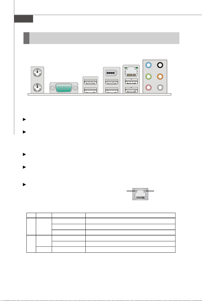
Back panel
- 1 PS/2 mouse port
- 1 PS/2 keyboard port
- 1 Serial port
- 6 USB 2.0 Ports
- 1 LAN jack
- 6 flexible audio jacks
- 1 1394 port (optional)
On-Board Pinheaders / Connectors / buttons
- 3 USB 2.0 pinheaders
- 1 1394 pinheader (optional)
- 1 chassis intrusion connector
- 1 S/PDIF-out pinheader
- 1 CD-in connector
- 1 front audio pinheader
- 1 TPM Module connector (optional)
- 1 Hardware Overclock FSB Switch
- 1 Reset button (optional)
- 1 Power button (optional)
- 1 Clear CMOS button (optional)
TPM (optional)
- Supports TPM
Slots
- 1 PCI Express x16 slot, support up to PCI Express 2.0 x16 speed
- 2 PCI Express x1 slots
- 3 PCI slots, support 3.3V/ 5V PCI bus Interface
Form Factor
- ATX (30.5cm X 24.5cm)
Mounting
- 9 mounting holes
English
En-3
Page 14
MS-7514 Mainboard
ON
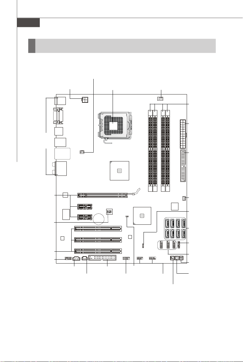
Quick Components Guide
SYSFAN2,
En-16
Back Panel,
En-12
PCIE,
En-24
OC_SW1,
En-23
PCI,
En-24
JAUD1,
En-19
PWR1, En-11
JCD1,
En-18
JSP1,
En-17
CPU, En-5
123
FDD1,
En-14
JCI1, En-16
J1394_1,
En-17
CPUFAN1, En-16
JFP2, JFP1
En-18
CLR_CMOS1,
En-22
DDR2 DIMMs,
En-9
JPWR1,
En-11
IDE1,
En-14
SYSFAN1,
En-16
JBAT1,
En-21
SATA,
En-15
JTPM1,
En-19
JUSB1~3,
En-20
RESET1,
En-22
POWER1,
En-22
En-4
Page 15
CPU (Central Processing Unit)
When you are installing the CPU, make sure to install the cooler to prevent
overheating. If you do not have the CPU cooler, consult your dealer before turning
on the computer.
For the latest information about CPU, please visit http://global.msi.com.tw/index.
php?func=cpuform
Important
Overheating
Overheating will seriously damage the CPU and system. Always make sure
the cooling fan can work properly to protect the CPU from overheating. Make
sure that you apply an even layer of thermal paste (or thermal tape) between
the CPU and the heatsink to enhance heat dissipation.
Replacing the CPU
While replacing the CPU, always turn off the ATX power supply or unplug the
power supply’s power cord from the grounded outlet first to ensure the safety
of CPU.
Overclocking
This mainboard is designed to support overclocking. However, please make
sure your components are able to tolerate such abnormal setting, while
doing overclocking. Any attempt to operate beyond product specifications is
not recommended. We do not guarantee the damages or risks caused
by inadequate operation or beyond product specifications.
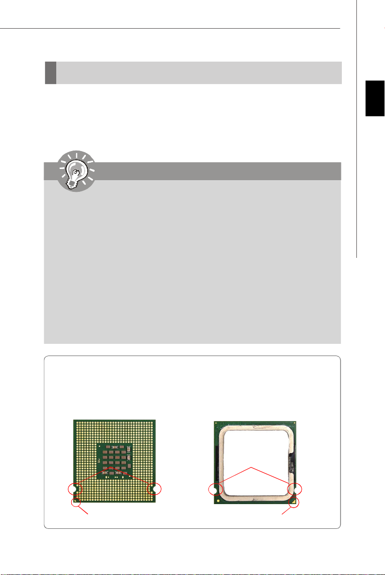
Introduction to LGA 775 CPU
The pin-pad side of LGA 775
CPU.
The surface of LGA 775 CPU.
Remember to apply some thermal paste on it for better heat
dispersion.
English
Alignment Key Alignment Key
Yellow triangle is the Pin 1 indicator
Yellow triangle is the Pin 1 indicator
En-5
Page 16
MS-7514 Mainboard
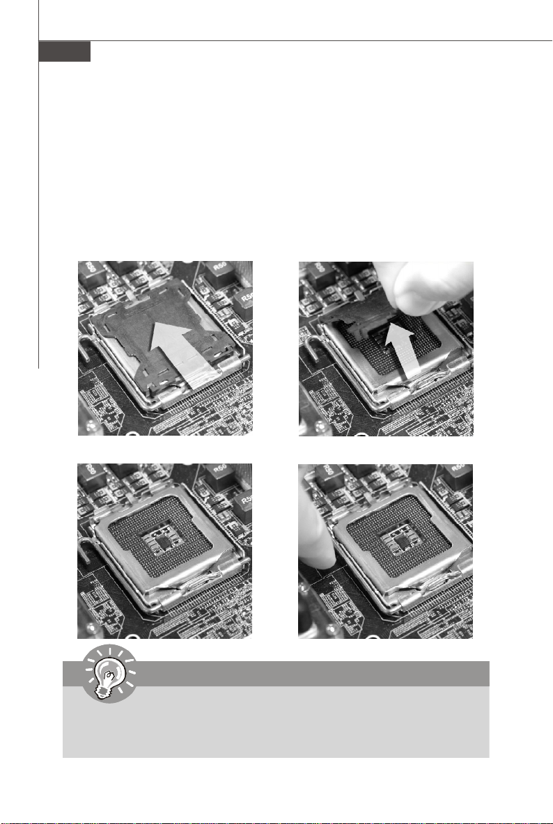
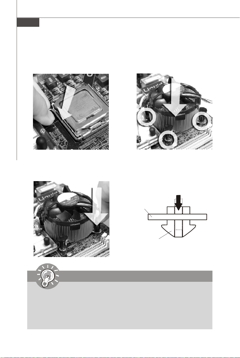
CPU & Cooler Installation
When you are installing the CPU, make sure the CPU has a cooler attached on
the top to prevent overheating. Meanwhile, do not forget to apply some thermal
paste on CPU before installing the heat sink/cooler fan for better heat dispersion.
Follow the steps below to install the CPU & cooler correctly. Wrong installation will
cause the damage of your CPU & mainboard.
1.The CPU socket has a plastic cap
on it to protect the contact from
damage. Before you install the CPU,
always cover it to protect the socket
pin.
2.Remove the cap from lever hinge
side (as the arrow shows).
3.The pins of socket reveal.
4.Open the load lever.
Important
1.Confirm if your CPU cooler is firmly installed before turning on your system.
2. Do not touch the CPU socket pins to avoid damaging.
3. The availability of the CPU land side cover depends on your CPU packing.
En-6
Page 17
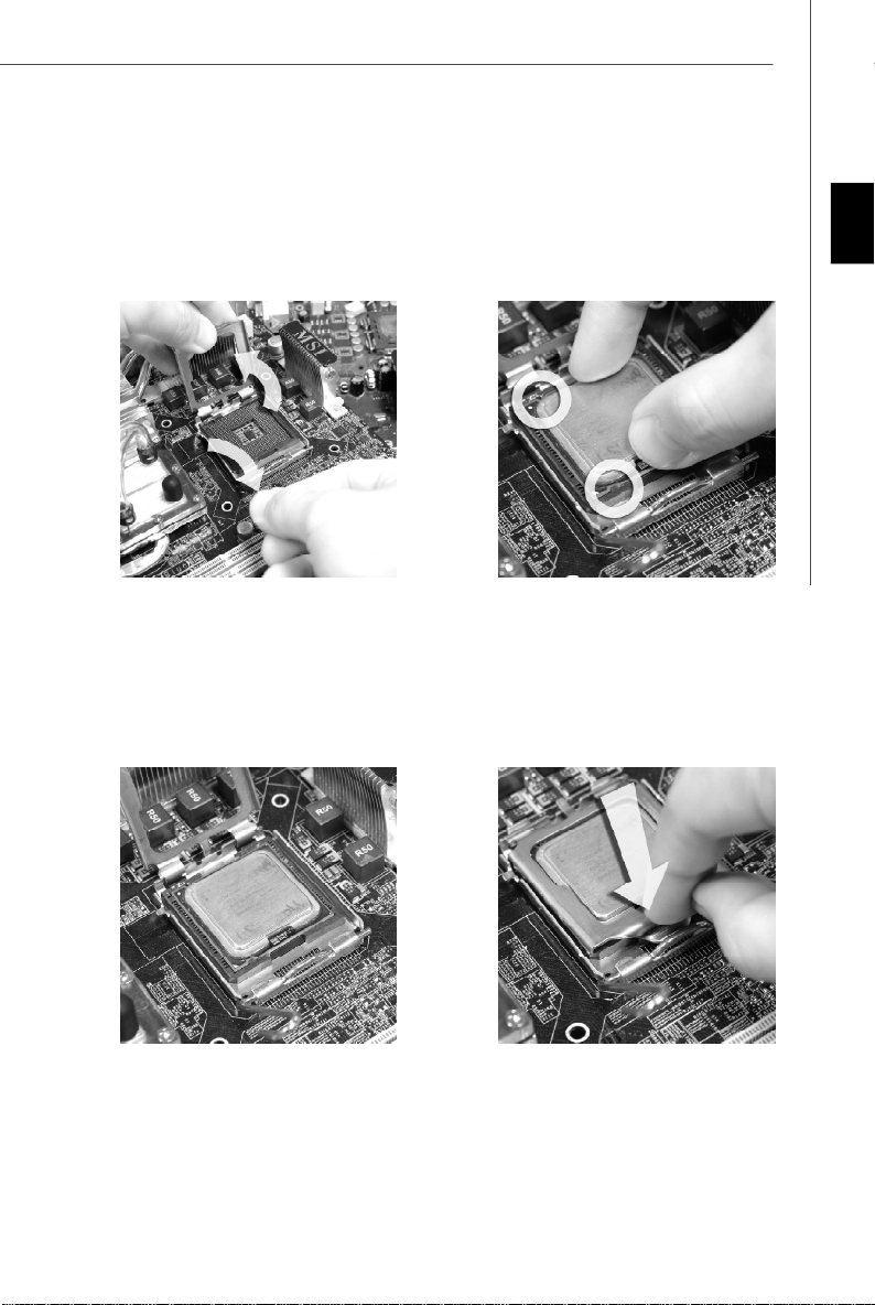
5.Lift the load lever up and open the
load plate.
6.After confirming the CPU direction
for correct mating, put down the
CPU in the socket housing frame.
Be sure to grasp on the edge of
the CPU base. Note that the alignment keys are matched.
alignment
key
English
7.Visually inspect if the CPU is
seated well into the socket. If not,
take out the CPU with pure vertical
motion and reinstall.
8.Cover the load plate onto the
package.
En-7
Page 18
MS-7514 Mainboard
9.Press down the load lever lightly
onto the load plate, and then secure the lever with the hook under
retention tab.
11.Press the four hooks down to fasten
the cooler. Then rotate the locking
switch (refer to the correct direction
marked on it) to lock the hooks.
10. Align the holes on the mainboard
with the heatsink. Push down the
cooler until its four clips get
wedged into the holes of the
mainboard.
12.Turn over the mainboard to confirm that the clip-ends are correctly
inserted.
Mainboard
locking
switch
Hook
Important
1. Read the CPU status in BIOS.
2. Whenever CPU is not installed, always protect your CPU socket pin with the
plastic cap covered (shown in Figure 1) to avoid damaging.
3. Mainboard photos shown in this section are for demonstration of the CPU/
cooler installation only. The appearance of your mainboard may vary depending on the model you purchase.
En-8
Page 19
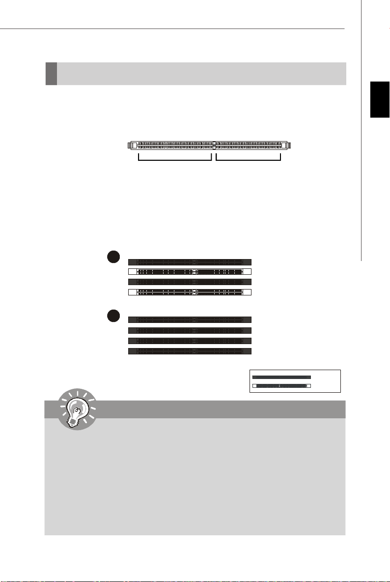
Memory
1
2
Installed
These DIMM slots are used for installing memory modules.
For more information on compatible components, please visit http://global.msi.com.
tw/index.php?func=testreport
DDR2
240-pin, 1.8V
56x2=112 pin64x2=128 pin
Dual-Channel Memory Population Rules
In Dual-Channel mode, the memory modules can transmit and receive data with two
data bus lines simultaneously. Enabling Dual-Channel mode can enhance the system
performance. Please refer to the following illustrations for population rules under
Dual-Channel mode.
DIMM1
DIMM2
DIMM3
DIMM4
DIMM1
DIMM2
DIMM3
DIMM4
English
Empty
Important
-DDR2 memory modules are not interchangeable with DDR and the DDR2
standard is not backwards compatible. You should always install DDR2
memory modules in the DDR2 DIMM slots.
-In Dual-Channel mode, make sure that you install memory modules of the
same type and density in different channel DIMM slots.
-To enable successful system boot-up, always insert the memory modules
into the DIMM1 first.
- Due to the chipset resource deployment, the system density will only be
detected up to 15+GB (not full 16GB) when each DIMM is installed with a
4GB memory module.
En-9
Page 20
MS-7514 Mainboard
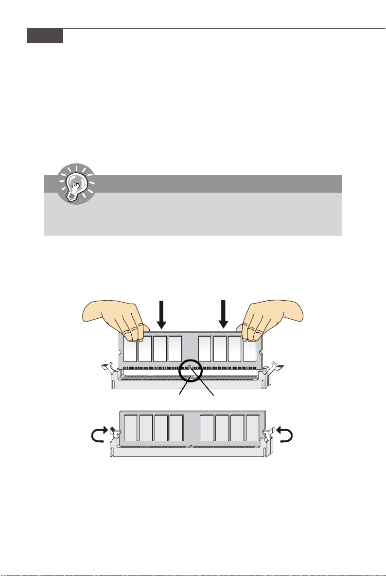
Installing Memory Modules
1. The memory module has only one notch on the center and will only fit in the right
orientation.
2. Insert the memory module vertically into the DIMM slot. Then push it in until the
golden finger on the memory module is deeply inserted in the DIMM slot. The plastic
clip at each side of the DIMM slot will automatically close when the memory module
is properly seated.
Important
You can barely see the golden finger if the memory module is properly inserted
in the DIMM slot.
3. Manually check if the memory module has been locked in place by the DIMM slot
clips at the sides.
En-10
Volt
Notch
Page 21
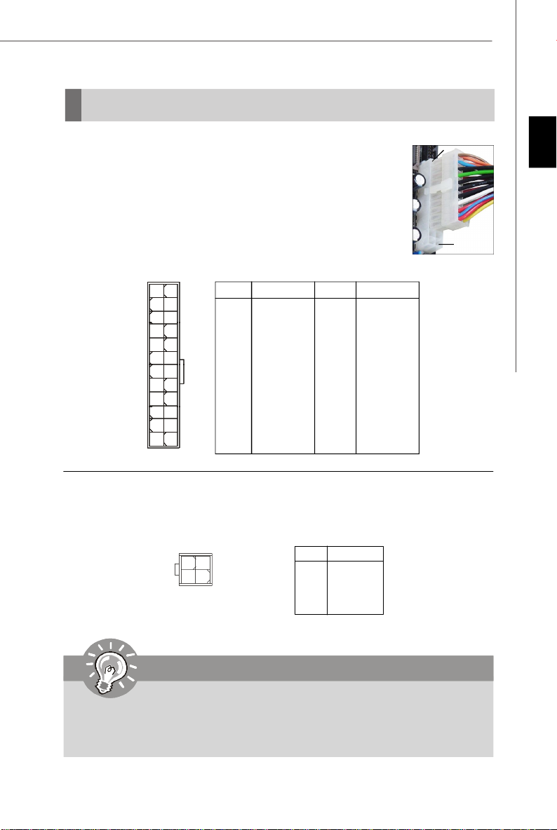
Power Supply
ATX 24-Pin Power Connector: JPWR1
This connector allows you to connect an ATX 24-pin power supply.
To connect the ATX 24-pin power supply, make sure the plug of the
power supply is inserted in the proper orientation and the pins are
aligned. Then push down the power supply firmly into the connector.
You may use the 20-pin ATX power supply as you like. If you’d like
to use the 20-pin ATX power supply, please plug your power supply along with pin 1 & pin 13 (refer to the image at the right hand).
Pin Definition
PIN SIGNAL
13 +3.3V
14 -12V
15 GND
16 PS-ON#
17 GND
18 GND
19 GND
20 Res
21 +5V
22 +5V
23 +5V
24 GND
JPWR1
12
1
24
13
PIN SIGNAL
1 +3.3V
2 +3.3V
3 GND
4 +5V
5 GND
6 +5V
7 GND
8 PWR OK
9 5VSB
10 +12V
11 +12V
12 +3.3V
ATX 4-pin Power Connector: PWR1
This power connector is used to provide power to the CPU.
Pin Definition
PIN SIGNAL
1 GND
2 GND
3 12V
4 12V
PWR1
2
4
13
pin 13
pin 12
English
Important
1. Make sure that all the connectors are connected to proper ATX power supplies to ensure stable operation of the mainboard.
2. Power supply of 400 watts (and above) is highly recommended for system
stability.
En-11
Page 22
MS-7514 Mainboard
Back Panel
Mouse
Keyboard
Serial Port
USB Port
(optional)
1394 Port
USB Port
LAN
USB Port
Line-In
Line-Out
Mic
RS-Out
CS-Out
SS-Out
Mouse/Keyboard
The standard PS/2® mouse/keyboard DIN connector is for a PS/2® mouse/keyboard.
Serial Port
The serial port is a 16550A high speed communications port that sends/ receives 16
bytes FIFOs. You can attach a serial mouse or other serial devices directly to the
connector.
1394 Port (optional)
The IEEE1394 port on the back panel provides connection to IEEE1394 devices.
USB Port
The USB (Universal Serial Bus) port is for attaching USB devices such as keyboard,
mouse, or other USB-compatible devices.
LAN
The standard RJ-45 LAN jack is for connection to
Green / OrangeYellow
the Local Area Network (LAN). You can connect a
network cable to it.
LED Color LED State Condition
Left Yellow On (steady state) LAN link is established.
Green Off 10 Mbit/sec data rate is selected.
Right On 100 Mbit/sec data rate is selected.
Orange On 1000 Mbit/sec data rate is selected.
Off LAN link is not established.
On (brighter & pulsing)The computer is communicating with another computer on the LAN.
En-12
Page 23

Audio Ports
These audio connectors are used for audio devices. It is easy to differentiate between audio effects according to the color of audio jacks.
Line-In (Blue) - Line In is used for external CD player, tapeplayer or
other audio devices.
Line-Out (Green) - Line Out, is a connector for speakers or headphones.
Mic (Pink) - Mic, is a connector for microphones.
RS-Out (Black) - Rear-Surround Out in 4/ 5.1/ 7.1 channel mode.
CS-Out (Orange) - Center/ Subwoofer Out in 5.1/ 7.1 channel mode.
SS-Out (Gray) - Side-Surround Out 7.1 channel mode.
English
En-13
Page 24
MS-7514 Mainboard
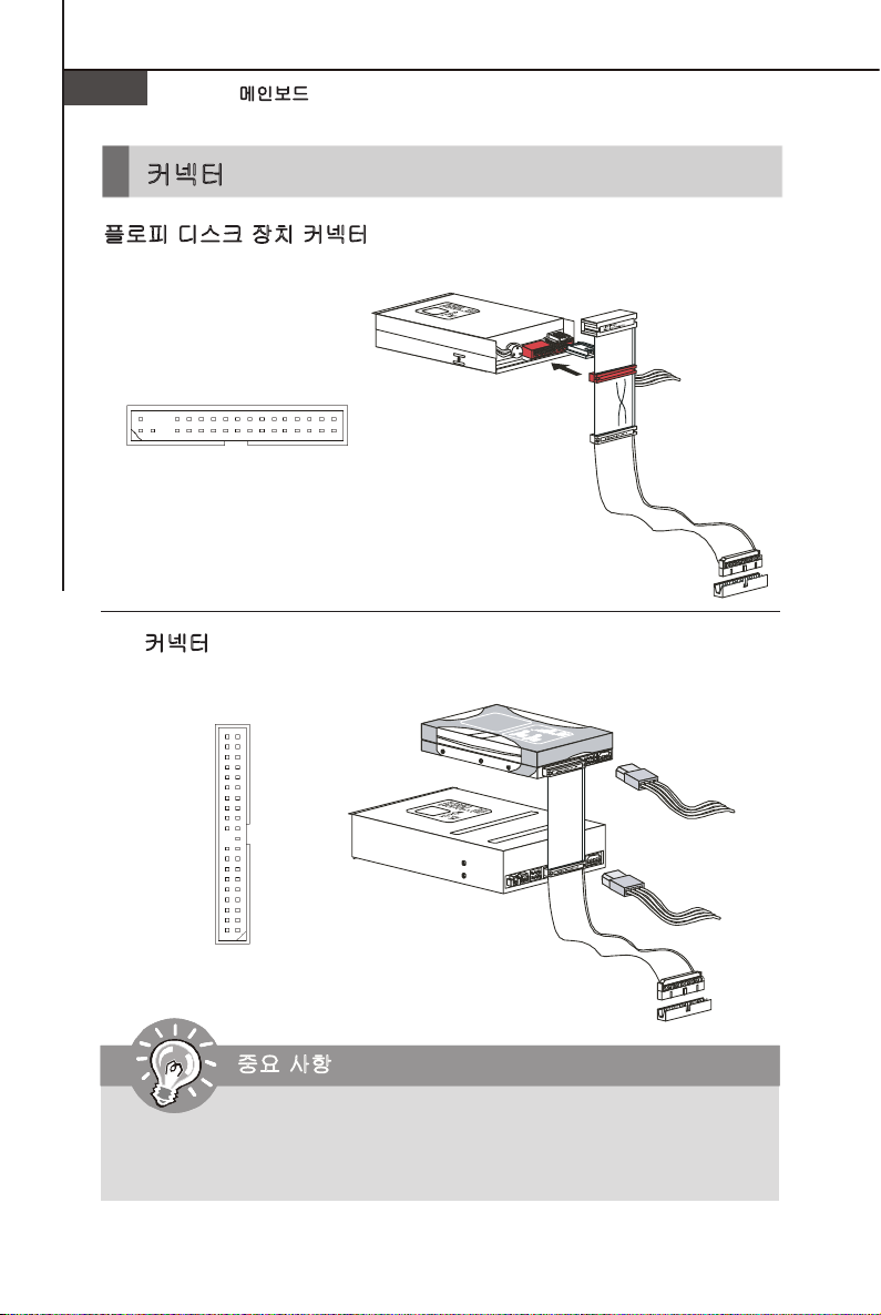
Connectors
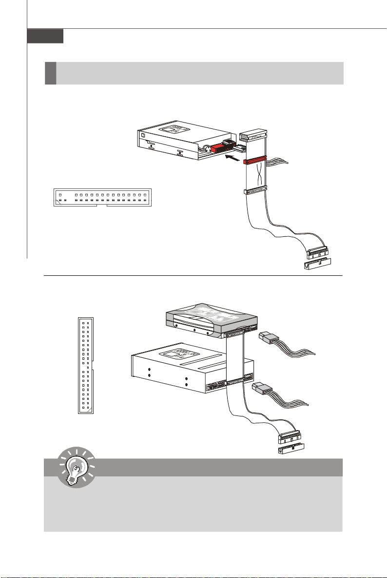
Floppy Disk Drive Connector: FDD1
This connector supports 360KB, 720KB, 1.2MB, 1.44MB or 2.88MB floppy disk drive.
IDE Connector: IDE1
This connector supports IDE hard disk drives, optical disk drives and other IDE devices.
Important
If you install two IDE devices on the same cable, you must configure the
drives separately to master / slave mode by setting jumpers. Refer to IDE
device’s documentation supplied by the vendors for jumper setting
instructions.
En-14
Page 25
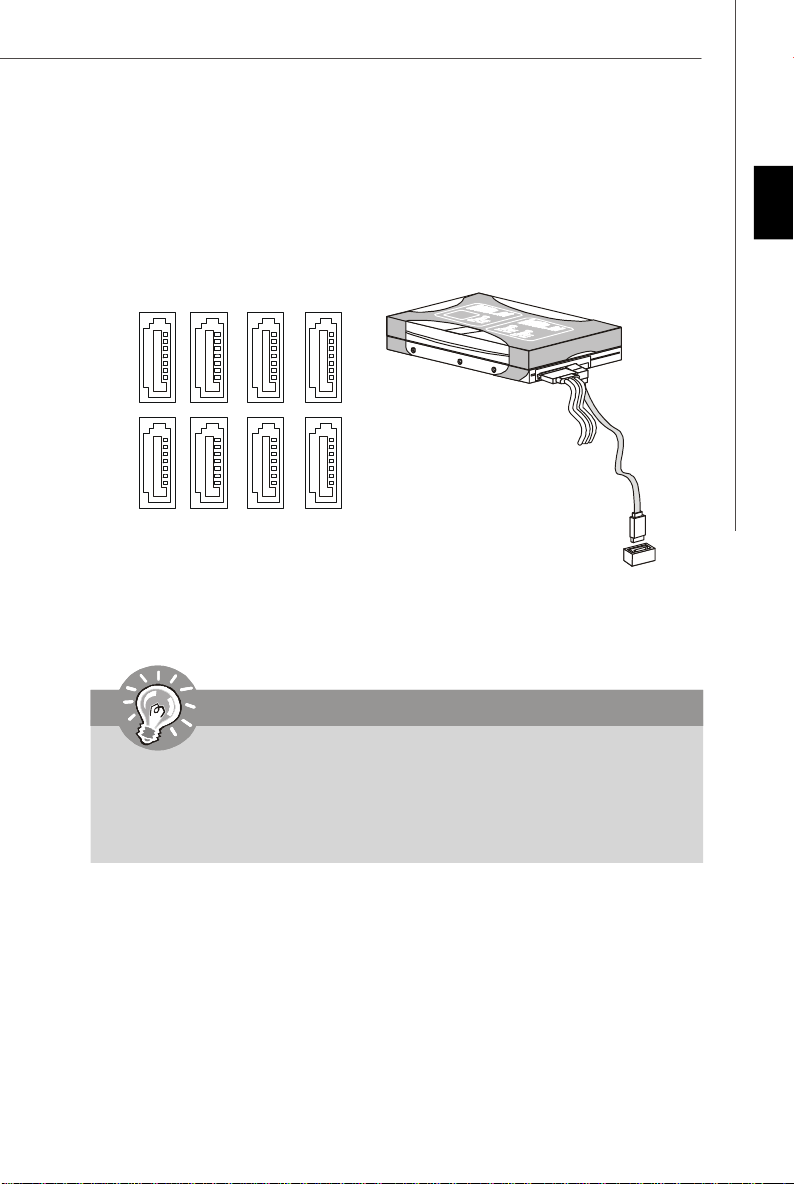
Serial ATA Connector: SATA1~8
This connector is a high-speed Serial ATA interface port. Each connector can
connect to one Serial ATA device.
English
SATA6 SATA2
SATA5
SATA4
SATA3
SATA1
SATA8
SATA7
Important
1. Please do not fold the Serial ATA cable into 90-degree angle. Otherwise,
data loss may occur during transmission.
2. SATA1~6 controlled by ICH10R/ ICH10, and the ICH10R supports RAID 0/
1/ 0+1/ 5 mode.
3. SATA7~8 controlled by JMB363 and they support RAID 0/ 1 mode.
En-15
Page 26
MS-7514 Mainboard
Fan Power Connectors: CPUFAN1, SYSFAN1~2
The fan power connectors support system cooling fan with +12V. When connecting
the wire to the connectors, always note that the red wire is the positive and should
be connected to the +12V; the black wire is Ground and should be connected to GND.
If the mainboard has a System Hardware Monitor chipset on-board, you must use a
specially designed fan with speed sensor to take advantage of the CPU fan control.
GND
NC
SENSOR
+12V
CONTROL
CPUFAN1
GND
SENSOR
+12V
GND
SYSFAN1
+12V
SYSFAN2
Important
1.Please refer to the recommended CPU fans at processor’s official website
or consult the vendors for proper CPU cooling fan.
2.CPUFAN1 supports fan control. You can install Dual Core Center utility
that will automatically control the CPU fan speed according to the actual
CPU temperature.
3. Fan cooler set with 3 or 4 pins power connector are both available for
CPUFAN1.
Chassis Intrusion Connector: JCI1
This connector connects to the chassis intrusion switch cable. If the chassis is
opened, the chassis intrusion mechanism will be activated. The system will record
this status and show a warning message on the screen. To clear the warning, you
must enter the BIOS utility and clear the record.
2
1
CINTRU
En-16
GND
JCI1
Page 27
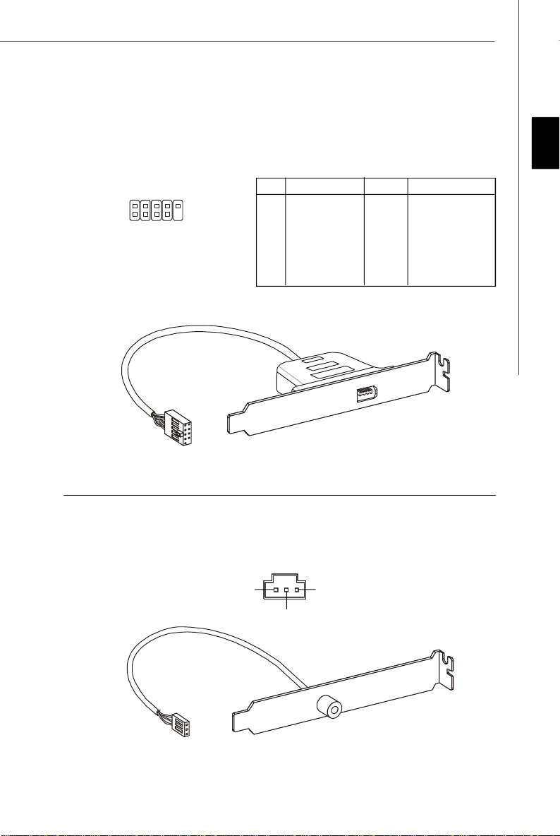
IEEE1394 Connector: J1394_1 (optional)
This connector allows you to connect the IEEE1394 device via an optional IEEE1394
bracket.
Pin Definition
PIN SIGNAL PIN SIGNAL
2
1
J1394_1
9
10
1 TPA+ 2 TPA-
3 Ground 4 Ground
5 TPB+ 6 TPB-
7 Cable power 8 Cable power
9 Key (no pin) 10 Ground
IEEE1394 Bracket (optional)
S/PDIF-Out Connector: JSP1
This connector is used to connect S/PDIF (Sony & Philips Digital Interconnect Format)
interface for digital audio transmission.
JSP1
English
VCC
GND
SPDIF
S/PDIF Bracket (optional)
En-17
Page 28
MS-7514 Mainboard
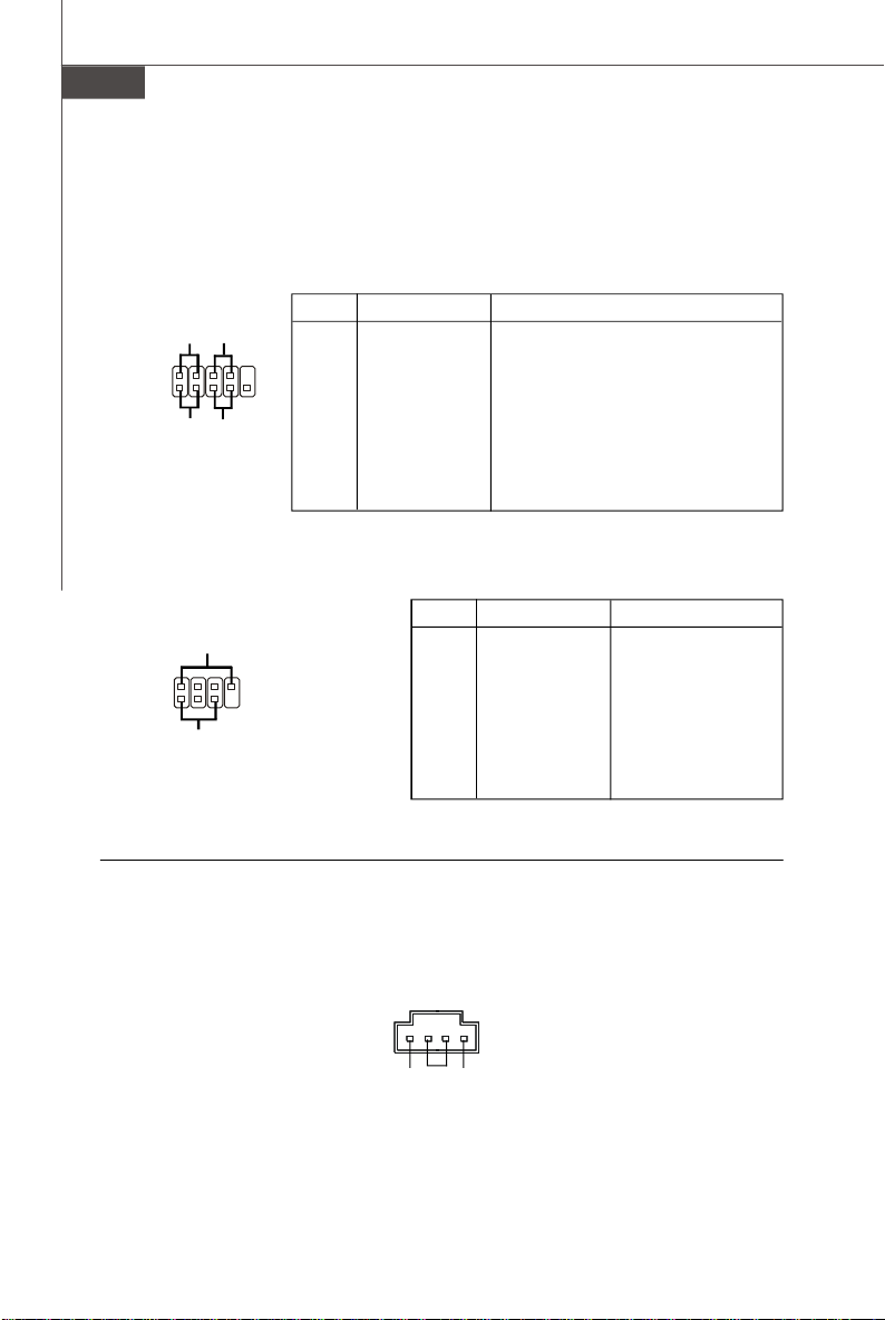
Front Panel Connectors: JFP1, JFP2
These connectors are for electrical connection to the front panel switches and LEDs.
The JFP1 is compliant with Intel® Front Panel I/O Connectivity Design Guide.
JFP1 Pin Definition
PIN SIGNAL DESCRIPTION
1 HD_LED + Hard disk LED pull-up
2 FP PWR/SLP MSG LED pull-up
3 HD_LED - Hard disk active LED
10
9
4 FP PWR/SLP MSG LED pull-up
5 RST_SW - Reset Switch low reference pull-down to GND
6 PWR_SW + Power Switch high reference pull-up
7 RST_SW + Reset Switch high reference pull-up
8 PWR_SW - Power Switch low reference pull-down to GND
9 RSVD_DNU Reserved. Do not use.
JFP2 Pin Definition
PIN SIGNAL DESCRIPTION
1 GND Ground
2 SPK- Speaker-
8
7
3 SLED Suspend LED
4 BUZ+ Buzzer+
5 PLED Power LED
6 BUZ- Buzzer-
7 NC No connection
8 SPK+ Speaker+
JFP1
JFP2
Power
LED
2
1
2
1
+
- -
HDD
LED
Speaker
+
Power
LED
Power
Switch
-
+
+
Reset
Switch
+
-
CD-In Connector: JCD1
This connector is provided for external audio input.
JCD1
R
L
GND
En-18
Page 29
Front Panel Audio Connector: JAUD1
This connector allows you to connect the front panel audio and is compliant with
Intel® Front Panel I/O Connectivity Design Guide.
JAUD1
9
10
HD Audio Pin Definition
PIN SIGNAL DESCRIPTION
1 MIC_L Microphone - Left channel
2 GND Ground
3 MIC_R Microphone - Right channel
4 NC
5 LINE out_R Analog Port - Right channel
6 MIC_JD Jack detection return from front panel microphone JACK1
7 Front_JD Jack detection sense line from the High Definition Audio CODEC
8 NC No control
9 LINE out_L Analog Port - Left channel
10 LINEout_JD Jack detection return from front panel JACK2
jack detection resistor network
1
2
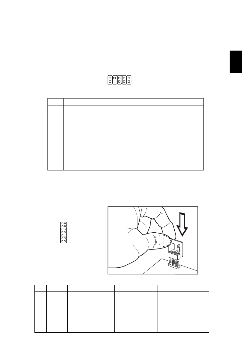
TPM Module Connector: JTPM1 (optinoal)
This connector connects to a TPM (Trusted Platform Module) module (optional). Please
refer to the TPM security platform manual for more details and usages.
21
English
1413
Pin Signal Description Pin Signal Description
1 LCLK LPC clock 2 3V_STB 3V standby power
3 LRST# LPC reset 4 VCC3 3.3V power
5 LAD0 LPC address & data pin0 6 SIRQ Serial IRQ
7 LAD1 LPC address & data pin1 8 VCC5 5V power
9 LAD2 LPC address & data pin2 10 KEY No pin
11 LAD3 LPC address & data pin3 12 GND Ground
13 LFRAME# LPC Frame 14 GND Ground
En-19
Page 30
MS-7514 Mainboard
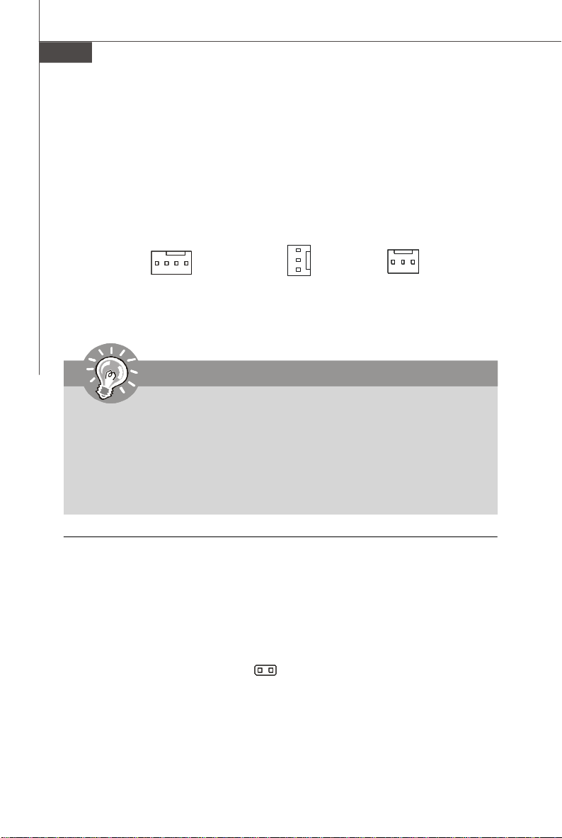
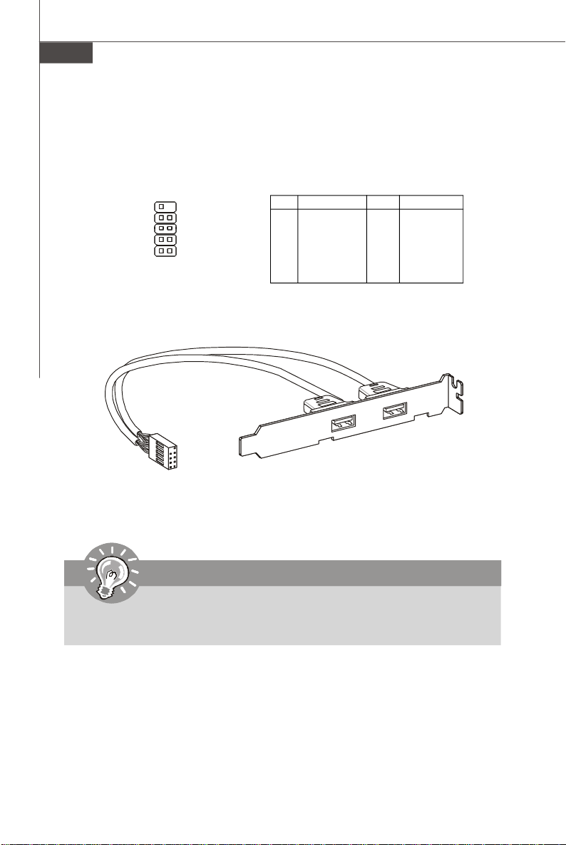
Front USB Connector: JUSB1~3
These connectors, compliant with Intel® I/O Connectivity Design Guide, is ideal for
connecting high-speed USB interface peripherals such as USB HDD, digital cameras,
MP3 players, printers, modems and the like.
Pin Definition
9
10
1 2
JUSB1~3
PIN SIGNAL PIN SIGNAL
1 VCC 2 VCC
3 USB0- 4 USB1-
5 USB0+ 6 USB1+
7 GND 8 GND
9 Key (no pin) 10 NC
USB 2.0 Bracket
(optional)
Important
Note that the pins of VCC and GND must be connected correctly to avoid
possible damage.
En-20
Page 31

Jumper
Clear CMOS Jumper: JBAT1
There is a CMOS RAM onboard that has a power supply from an external battery to
keep the data of system configuration. With the CMOS RAM, the system can automatically boot OS every time it is turned on. If you want to clear the system configuration,
set the jumper to clear data.
3
1
Clear Data
1
JBAT1
3
1
Keep Data
Important
You can clear CMOS by shorting 2-3 pin while the system is off. Then return
to 1-2 pin position. Avoid clearing the CMOS while the system is on; it will
damage the mainboard.
English
En-21
Page 32

MS-7514 Mainboard
Buttons
The motherboard provides the following buttons(optinoal) for you to set the computer’s
function. This section will explain how to change your motherboard’s function through
the use of button.
Power Button: POWER1 (optional)
This power button is used to turn-on or turn-off the system. Press the button to turnon or turn-off the system.
POWER1
Reset Button: RESET1 (optional)
This reset button is used to reset the system. Press the button to reset the system.
RESET1
Clear CMOS Button: CLR_CMOS1 (optional)
There is a CMOS RAM onboard that has a power supply from an external battery to
keep the data of system configuration. With the CMOS RAM, the system can automatically boot OS every time it is turned on. If you want to clear the system configuration,
simply press the button to clear data.
CLR_CMOS1
Important
Make sure that you power off the system before press the clear CMOS button.
En-22
Page 33

Switch
Hardware Overclock FSB Switch: OC_SW1
You can overclock the FSB to increase the processor frequency by changing the
switch OC_SW1. Follow the instructions below to set the FSB.
ON
123
Default
ON
123
200->266 MHz 200->333 MHz 200->400 MHz
ON
123
ON
123
266->333 MHz
ON
123
266->400 MHz
333->400 MHz
Important
1. Make sure that you power off the system before changing the switch.
2. Overclocking may cause instability or crash during boot, then please set
the switch to default setting.
English
En-23
Page 34

MS-7514 Mainboard
Slots
PCI (Peripheral Component Interconnect) Express Slot
The PCI Express slot supports the PCI Express interface expansion card.
The PCI Express 2.0 x16 supports up to 8.0 GB/s transfer rate.
The PCI Express x1 supports up to 250 MB/s transfer rate.
PCI Express x16 Slot
PCI Express x 1 Slot
PCI (Peripheral Component Interconnect) Slot
The PCI slot supports LAN card, SCSI card, USB card, and other add-on cards that
comply with PCI specifications.
32-bit PCI Slot
Important
When adding or removing expansion cards, make sure that you unplug the
power supply first. Meanwhile, read the documentation for the expansion card
to configure any necessary hardware or software settings for the expansion
card, such as jumpers, switches or BIOS configuration.
PCI Interrupt Request Routing
The IRQ, acronym of interrupt request line and pronounced I-R-Q, are hardware lines
over which devices can send interrupt signals to the microprocessor. The PCI IRQ
pins are typically connected to the PCI bus pins as follows:
Order 1 Order 2 Order 3 Order 4
PCI Slot 1 INT A# INT B# INT C# INT D#
PCI Slot 2 INT E# INT F# INT G# INT H#
PCI Slot 3 INT F# INT G# INT H# INT E#
En-24
Page 35

LED Status Indicators
ON
123
LED3 LED1
LED2
LED4
English
Blue Light Off
LED4 LED3 LED2 LED1 Mode
CPU is in 1 phase power mode.
CPU is in 2 phase power mode.
CPU is in 3 phase power mode.
CPU is in 4 phase power mode.
En-25
Page 36

MS-7514 Mainboard
BIOS Setup
This chapter provides basic information on the BIOS Setup program and allows you
to configure the system for optimum use. You may need to run the Setup program
when:
* An error message appears on the screen during the system booting up, and requests
you to run BIOS SETUP.
* You want to change the default settings for customized features.
Important
1.The items under each BIOS category described in this chapter are under
continuous update for better system performance. Therefore, the description
may be slightly different from the latest BIOS and should be held for reference
only.
2.Upon boot-up, the 1st line appearing after the memory count is the BIOS
version. It is usually in the format:
A7514IMS V2.0 082208 where:
1st digit refers to BIOS maker as A = AMI, W = AWARD, and P = PHOENIX.
2nd - 5th digit refers to the model number.
6th refers to the Chipset vender as A = AMD, I = Intel, V = VIA, N = Nvidia, U =
ULi.
7th - 8th digit refers to the customer as MS = all standard customers.
V2.0 refers to the BIOS version.
082208 refers to the date this BIOS was released.
En-26
Page 37

Entering Setup
Power on the computer and the system will start POST (Power On Self Test) process.
When the message below appears on the screen, press <DEL> key to enter Setup.
Press DEL to enter SETUP
If the message disappears before you respond and you still wish to enter Setup,
restart the system by turning it OFF and On or pressing the RESET button. You may
also restart the system by simultaneously pressing <Ctrl>, <Alt>, and <Delete> keys.
Getting Help
After entering the Setup menu, the first menu you will see is the Main Menu.
Main Menu
The main menu lists the setup functions you can make changes to. You can use the
arrow keys (↑↓ ) to select the item. The on-line description of the highlighted setup
function is displayed at the bottom of the screen.
Sub-Menu
If you find a right pointer symbol (as shown in the right view)
appears to the left of certain fields that means a sub-menu
containing additional options can be launched from this field.
You can use control keys (↑↓ ) to highlight the field and
press <Enter> to call up the sub-menu. Then you can use the
control keys to enter values and move from field to field within a sub-menu. If you
want to return to the main menu, just press <Esc >.
General Help <F1>
The BIOS setup program provides a General Help screen. You can call up this screen
from any menu by simply pressing <F1>. The Help screen lists the appropriate keys
to use and the possible selections for the highlighted item. Press <Esc> to exit the
Help screen.
English
En-27
Page 38

MS-7514 Mainboard
The Main Menu
Once you enter AMI® or AWARD® BIOS CMOS Setup Utility, the Main Menu will appear
on the screen. The Main Menu allows you to select from ten setup functions and two
exit choices. Use arrow keys to select among the items and press <Enter> to accept
or enter the sub-menu.
Standard CMOS Features
Use this menu for basic system configurations, such as time, date etc.
Advanced BIOS Features
Use this menu to setup the items of special enhanced features.
Integrated Peripherals
Use this menu to specify your settings for integrated peripherals.
Power Management Setup
Use this menu to specify your settings for power management.
H/W Monitor
This entry shows your PC health status.
GreenPower
Use this menu to specify the power phase.
BIOS Setting Password
Use this menu to set the Password.
Cell Menu
Use this menu to specify your settings for frequency/voltage control and overclocking.
USER SETTINGS
Use this menu to save/ load your settings to/ from CMOS for BIOS.
Load Fail-Safe Defaults
Use this menu to load the default values set by the BIOS vendor for stable system
performance.
Load Optimized Defaults
Use this menu to load the default values set by the mainboard manufacturer specifically
for optimal performance of the mainboard.
Save & Exit Setup
Save changes to CMOS and exit setup.
Exit Without Saving
Abandon all changes and exit setup.
En-28
Page 39

When enter the BIOS Setup utility, follow the processes below for general use.
1. Load Optimized Defaults : Use control keys (↑↓) to highlight the Load
Optimized Defaults field and press <Enter> , a message as below appears:
Select [Ok] and press Enter to load the default settings for optimal system
performance.
2. Setup Date/ Time : Select the Standard CMOS Features and press <Enter> to
enter the Standard CMOS Features-menu. Adjust the Date, Time fields.
3. Save & Exit Setup : Use control keys (↑↓) to highlight the Save & Exit Setup
field and press <Enter> , a message as below appears:
English
Select [Ok] and press Enter to save the configurations and exit BIOS Setup utility.
Important
The configuration above are for general use only. If you need the detailed
settings of BIOS, please read the manual in English version on MSI website.
En-29
Page 40

MS-7514 Mainboard
4. Cell Menu Introduction : This menu is for advanced user who want to overclock
the mainboard.
Important
Change these settings only if you are familiar with the chipset.
Current CPU / DRAM Frequency
These items show the current clocks of CPU and Memory speed. Read-only.
Multi-step OC Booster
This item is used to avoid the BIOS might crash with overclocking.
Disabled Disable this item, apply OC settings during POST.
Mode 1 Slight OC during POST and then apply full OC when loading
Mode 2 Load the OS then apply the OC settings.
En-30
the OS
Page 41

D.O.T. Control
D.O.T. (Dynamic Overclocking Technology) is an automatic overclocking function,
included in the MSITM’s newly developed Dual CoreCell
TM
Technology. It is designed to
detect the load balance of CPU while running programs, and to adjust the best
frequency automatically. When the mainboard detects system is running programs, it
will speed up automatically to make the program run smoothly and faster. When the
system is temporarily suspending or staying in the low load balance, it will restore the
default settings instead. Usually the Dynamic Overclocking Technology will be powered only when users' PC need to run huge amount of data like 3D games or the video
process, and the CPU and PCIE frequency need to be boosted up to enhance the
overall performance.
Important
Even though the Dynamic Overclocking Technology is more stable than
manual overclocking, basically, it is still risky. We suggest user to make
sure that your CPU / memory modules can afford to overclocking regularly
first. If you find the PC appears to be unstable or reboot incidentally, it's
better to disable the Dynamic Overclocking or to lower the level of
overclocking options. By the way, if you need to conduct overclocking
manually, you also need to disable the Dynamic OverClocking first.
Intel EIST
The Enhanced Intel SpeedStep technology allows you to set the performance level of
the microprocessor whether the computer is running on battery or AC power. This
field will appear after you installed the CPU which support speedstep technology.
English
Adjust CPU FSB Frequency (MHz)
This item allows you to set the CPU FSB frequency (in MHz).
Adjust CPU Ratio
This item lets you to adjust the CPU ratio. It is available only when the processor
supports this function.
Adjusted CPU Frequency (MHz)
It shows the adjusted CPU frequency (FSB x Ratio). Read-only.
En-31
Page 42

MS-7514 Mainboard
Advance DRAM Configuration
Press <Enter> to enter the sub-menu and the following screen appears.
MEMORY-Z
Press <Enter> to enter the sub-menu and the following screen appears.
DIMM1~4 Memory SPD Infromation
Press <Enter> to enter the sub-menu and the following screen appears.
DIMM1~4 Memory SPD Infromation
These items display the current status of the current DIMM Memory speed
information such as memory type, max bandwidth, manufacture, part number,
serial number, SDRAM cycle time, DRAM TCL, DRAM TRCD, DRAM TRP, DRAM
TRAS, DRAM TRFC, DRAM TWR, DRAM TWTR, DRAM TRRD and DRAM TRTP.
They are read only.
CAS# Latency (CL)
This controls the CAS latency, which determines the timing delay (in clock cycles)
before SDRAM starts a read command after receiving it.
tRCD
When DRAM is refreshed, both rows and columns are addressed separately.
This setup item allows you to determine the timing of the transition from RAS
(row address strobe) to CAS (column address strobe). The less the clock
cycles, the faster the DRAM performance.
tRP
This setting controls the number of cycles for Row Address Strobe (RAS) to be
allowed to precharge. If insufficient time is allowed for the RAS to accumulate its
charge before DRAM refresh, refresh may be incomplete and DRAM may fail to
retain data. This item applies only when synchronous DRAM is installed in the
system.
tRAS
This setting determines the time RAS takes to read from and write to memory
cell.
1N/2N Memory Timing
This item controls the SDRAM command rate. Select [1N] makes SDRAM signal
controller to run at 1N (N=clock cycles) rate. Selecting [2N] makes SDRAM signal
controller run at 2N rate.
Advance Memory Setting
Setting to [Auto] enables the advance memory timing automatically to be determined
by BIOS. Setting to [Manual] allows you to set advanced memory timings.
En-32
Page 43

TRFC
When the Advance Memory Setting sets to [Manual], the field is adjustable.
This setting determines the time RFC takes to read from and write to a memory
cell.
TWR
When the Advance Memory Setting sets to [Manual], the field is adjustable.
Minimum time interval between end of write data burst and the start of a
precharge command. Allows sense amplifiers to restore data to cells.
TWTR
When the Advance Memory Setting sets to [Manual], the field is adjustable.
Minimum time interval between the end of write data burst and the start of a
column-read command. It allows I/O gating to overdrive sense amplifiers before
read command starts.
TRRD
When the Advance Memory Setting sets to [Manual], the field is adjustable.
Specifies the active-to-active delay of different banks.
TRTP
When the Advance Memory Setting sets to [Manual], the field is adjustable.
Time interval between a read and a precharge command.
CHA TRD/ TRD2RD/ TWR2WR/ TWR2RD/ /TWD2WR/ TRD Phase
When the Advance Memory Setting sets to [Manual], these fields are
adjustable. These items is used to set the memory timings for memory channel
A.
CHB TRD/ TRD2RD/ TWR2WR/ TWR2RD/ TRD2WR/ TRD Phase
When the Advance Memory Setting sets to [Manual], these fields are
adjustable. These items is used to set the memory timings for memory channel
B.
FSB/DRAM Ratio
This item will allow you to adjust the ratio of FSB to memory.
Adjusted DRAM Frequency (MHz)
It shows the adjusted DDR Memory frequency. Read-only.
ClockGen Tuner
Press <Enter> to enter the sub-menu.
CPU Clock Drive/ PCI Express Clock Drive
These items are used to select the CPU/ PCI Express clock amplitude.
CPU CLK Skew/ MCH CLK Skew
These items are used to select the CPU/ North Bridge chipset clock skew. They
can help CPU to reach the higher overclocking performace.
English
En-33
Page 44

MS-7514 Mainboard
Adjust PCI Frequency (MHz)
This field allows you to select the PCI frequency (in MHz).
Auto Disable DRAM/PCI Frequency
When set to [Enabled], the system will remove (turn off) clocks from empty DIMM and
PCI slots to minimize the electromagnetic interference (EMI).
CPU Voltage (V)/ CPU GTL REF0 / CPU GTL REF1 / DRAM Voltage (V)/ MCH
Voltage (V)/ MCH GTL REF / VTT FSB Voltage (V)/ ICH Voltage (V)
These items are used to asjust the voltage of CPU, Memory, FSB and chipset.
Spread Spectrum
When the mainboard’s clock generator pulses, the extreme values (spikes) of the
pulses create EMI (Electromagnetic Interference). The Spread Spectrum function
reduces the EMI generated by modulating the pulses so that the spikes of the pulses
are reduced to flatter curves. If you do not have any EMI problem, leave the setting at
Disabled for optimal system stability and performance. But if you are plagued by EMI,
set to Enabled for EMI reduction. Remember to disable Spread Spectrum if you are
overclocking because even a slight jitter can introduce a temporary boost in clock
speed which may just cause your overclocked processor to lock up.
Important
1.If you do not have any EMI problem, leave the setting at [Disabled] for
optimal system stability and performance. But if you are plagued by EMI,
select the value of Spread Spectrum for EMI reduction.
2.The greater the Spread Spectrum value is, the greater the EMI is reduced,
and the system will become less stable. For the most suitable Spread
Spectrum value, please consult your local EMI regulation.
3.Remember to disable Spread Spectrum if you are overclocking because
even a slight jitter can introduce a temporary boost in clock speed which
may just cause your overclocked processor to lock up.
En-34
Page 45

Software Information
Take out the Driver/Utility CD that is included in the mainboard package, and place it
into the CD-ROM drive. The installation will auto-run, simply click the driver or utility
and follow the pop-up screen to complete the installation. The Driver/Utility CD contains the:
Driver menu - The Driver menu shows the available drivers. Install the driver by your
desire and to activate the device.
Utility menu - The Utility menu shows the software applications that the mainboard
supports.
WebSite menu- The WebSite menu shows the necessary websites.
Important
Please visit the MSI website to get the latest drivers and BIOS for better
system performance.
English
En-35
Page 46

This page is intentionally left blank.
viii
Page 47

시리즈
사용 설명서
한국어
한국어
Kr-1
Page 48

MS-7514 메인보드
메인보드 사양
지원되는 프로세서
- LGA775 패키지의 Intel® Core 2 Extreme, Core 2 Quad, Core 2 Duo,
Pentium Dual-Core 및 Celeron Dual-Core 프로세서
- 차세대 Intel® 45 nm Multi-core CPU
*(CPU에 대한 최신 정보는 http://global.msi.com.tw/index.
php?func=cpuform 참조)
지원되는 FSB
- 1600*(OC)/ 1333/ 1066/ 800 MHz
칩셋
- 노스 브릿지: Intel® P45/ P43 칩셋
- 사우스 브릿지: Intel® ICH10/ ICH10R 칩셋
지원되는 메모리
- 4 DDR2 DIMM이 DDR2 1066**(OC)/ 800/ 667 SDRAM 지원(240핀 /
1.8V /최대 16GB)
** (호환 가능한 부품에 대한 자세한 내용은 http://global.msi.com.tw/
index.php?func=testreport를 참조하십시오.)
LAN
- Realtek 8111C에 의해 PCIE LAN 10/100/1000 고속 이더넷 지원
Kr-2
오디오
- Realtek® ALC888에 의해 통합된 칩
- 잭 감지 기능이 있는 플렉시블 8채널 오디오
- Azalia 1.0 규격 준수
- Microsoft Vista Premium 사양 충족
IDE
- JMicron JMB363에 의한 IDE 포트 1개
- Ultra DMA 66/100/133 모드 지원
- PIO, 버스 마스터 작동 모드 지원
SATA
- ICH10/ ICH10R에 의한 SATAII 포트 6개(SATA1~6)
- JMicron JMB363에 의한 SATAII 포트 2개(SATA7~8)
- 최대 3 Gb/s의 저장 및 데이터 전송 지원
RAID
- SATA1~6이 ICH10R에 의해 RAID 0/ 1/ 5/ 10/ JBOD 모드
- SATA7 및 SATA8이 JMicron에 의해 RAID 0/ 1/ JBOD 지원 JMB363
Page 49

1394 (옵션)
- JMicron JMB381이 1394 지원
FDD
- 플로피 포트 1개
- 360KB, 720KB, 1.2MB, 1.44MB 및 2.88MB의 FDD 1개 지원
커넥터
후면 패널
- PS/2 마우스 포트 1개
- PS/2 키보드 포트 1개
- 직렬 포트 1개
- USB 2.0 포트 6개
- LAN 잭 1개
- 플렉시블 오디오 잭 6개
- 1394 포트 1개(옵션)
온보드 핀헤더/커넥터/버튼
- USB 2.0 핀헤더 3개
- 1394 핀헤더 1개(옵션)
- 섀시 침입 커넥터 1개
- S/PDIF 출력 핀헤더 1개
- CD 입력 커넥터 1개
- 전면 오디오 핀헤더 1개
- TPM 모듈 커넥터 1개(옵션)
- 하드웨어 오버클록 FSB 스위치 1개
- 리셋 버튼 1개(옵션)
- 전원 버튼 1개(옵션)
- CMOS 지우기 버튼 1개(옵션)
TPM (옵션)
- TPM 지원
한국어
슬롯
- PCI Express x16 슬롯 1개, 최대 PCI Express 2.0 x16 속도 지원
- PCI Express x1 슬롯 2개
- PCI 슬롯 3개, 3.3V/5V PCI 버스 인터페이스 지원
폼 팩터
- ATX (30.5cm X 24.5cm)
장착
- 장착 구멍 9개
Kr-3
Page 50

MS-7514 메인보드
ON
1 2 3
빠른 부품 설명서
SYSFAN2,
Kr-16
Back Panel,
Kr-12
PCIE,
Kr-24
OC_SW1,
Kr-23
PCI,
Kr-24
JAUD1,
Kr-19
PWR1, Kr-11
JCD1,
Kr-18
JSP1,
Kr-17
CPU, Kr-5
FDD1,
Kr-14
JCI1, Kr-16
J1394_1,
Kr-17
CPUFAN1, Kr-16
JFP2, JFP1
Kr-18
CLR_CMOS1,
Kr-22
DDR2 DIMMs,
Kr-9
JPWR1,
Kr-11
IDE1,
Kr-14
SYSFAN1,
Kr-16
JBAT1,
Kr-21
SATA,
Kr-15
JTPM1,
Kr-19
JUSB1~3,
Kr-20
RESET1,
Kr-22
POWER1,
Kr-22
Kr-4
Page 51

CPU (중앙 처리 장치)
CPU 설치 시 과열을 방지하는 쿨러를 반드시 설치하십시오. CPU 쿨러가 없는 경우, 컴
퓨터를 켜기 전에 판매점에 문의하십시오.
CPU에 대한 최신 정보는
http://global.msi.com.tw/index.php?func=cpuform
참조
중요 사항
과열
과열은
CPU
록 냉각 팬이 제대로 작동하는지 항상 확인하십시오. 열이 잘 발산되도록
와 시스템을 심각하게 손상시킬 수 있습니다.
CPU
가 과열되지 않도
CPU
방열판 사이에 서멀 페이스트(또는 서멀 테이프)를 고르게 바르십시오.
CPU
교체
CPU
교체 시, 항상 전원을 끄거나 먼저
된 콘센트에서 뽑아
CPU
의 안전을 확보하십시오.
ATX
전원 공급장치의 전원 코드를 접지
오버클로킹
이 메인보드는 오버클로킹 기능을 지원하도록 디자인되었습니다. 그러나 오버
클로킹이 진행되는 동안 부품이 이러한 비정상적인 설정을 견뎌낼 수 있는지 확
인하십시오. 제품 사양을 초과하는 범위에서 작동시키지 마십시오. 당사는 올
바르지 않은 작동이나 제품 사양을 초과한 범위에서 사용하여 발생한 손상 또는
위험은 보증하지 않습니다.
LGA 775 CPU 소개
LGA 775 CPU 의 핀 패드 면
정렬 키
LGA 775 CPU의 표면.
열이 잘 발산되도록 서멀 페이스
트를 표면에 약간 바르십시오.
정렬 키
한국어
와
노란색 삼각형은 핀 1의 표시기입니다.
노란색 삼각형은 핀 1의 표시기입니다.
Kr-5
Page 52

MS-7514 메인보드
CPU 및 쿨러 설치
CPU 설치 시 과열을 방지하는 쿨러를 상단에 연결하십시오. 한편, 열이 잘 발산되도록
방열판/쿨러 팬을 설치하기 전에 CPU에 서멀 페이스트를 약간 바르십시오.
아래의 단계에 따라 CPU 및 쿨러를 올바로 설치하십시오. 잘못 설치할 경우 CPU와 메
인보드가 손상됩니다.
1. CPU 소켓에는 접촉에 의한 손상을
방지하는 플라스틱 캡이 있습니다.
CPU를 설치하기 전에, 항상 캡으로
소켓을 덮어 소켓 핀을 보호하십시
오.
2. 화살표와 같이 캡을 레버 힌지 쪽으
로부터 제거하십시오.
3. 소켓의 핀이 드러납니다.
중요 사항
1.
시스템을 켜기 전에
2.
손상을 방지하려면
3. CPU
Kr-6
랜드쪽 커버의 가용성은
CPU
4. 로드 레버를 엽니다.
CPU
쿨러가 단단히 설치되었는지 확인합니다.
소켓을 만지지 마십시오.
CPU
패킹에 따라 다릅니다.
Page 53

5. 로드 레버를 위로 올리고 로드 플레
이트를 엽니다.
6. CPU 방향이 올바로 맞춰졌는지 확
인한 다음, CPU를 소켓 하우징 프
레임에 내려 놓습니다. CPU 베이스
의 가장자리를 잡으십시오. 정렬 키
가 맞춰졌는지 유의하십시오.
한국어
정렬 키
7. CPU가 소켓에 제대로 앉혀졌는지
육안으로 검사합니다. 그렇지 않은
경우, CPU를 수직 방향으로 들어 올
린 다음 다시 설치합니다.
8. 로드 플레이트로 패키지를 덮습니
다.
Kr-7
Page 54

MS-7514 메인보드
9. 로드 레버를 로드 플레이트 위로 살
짝 누른 다음, 리텐션 탭 아래의 훅
을 사용하여 레버를 고정합니다.
11.4개의 훅을 눌러 쿨러를 고정합니다.
그리고 나서 잠금 스위치를 돌려 훅을
잠급니다(스위치에 표시된 올바른 방
향 참조).
10. 메인보드의 구멍을 방열판과 맞춥
니다. 4개의 클립이 메인보드의 구
멍에 완전히 박힐 때까지 쿨러를 누
릅니다.
12.메인보드를 뒤집어 클립 엔드가 올바
로 끼워졌는지 확인합니다.
메인보드
잠금 스위치
훅
중요 사항
1. BIOS에서 CPU
2. CPU
가 설치되어 있지 않은 경우, 손상되지 않도록 (그림 1과 같이) 항상 플라스
틱 캡으로
3.
이 절에 표시된 메인보드 사진은
진입니다. 메인보드의 외양은 구입한 모델에 따라 다를 수 있습니다.
Kr-8
상태를 읽습니다
CPU
소켓 핀을 보호하십시오.
.
CPU/
쿨러 설치를 보여줄 목적으로만 사용된 사
Page 55

메모리
⽸㛨G㢼㢀
㉘㾌╜
DIMM 슬롯은 메모리 모듈을 설치하는 데 사용됩니다.
호환 가능한 부품에 대한 자세한 내용은 http://global.msi.com.tw/index.
php?func=testreport를 참조하십시오.
DDR2
240 핀, 1.8V
64x2=128핀 56x2=112핀
듀얼 채널 모드 배포 규칙
듀얼 채널 모드에서는 메모리 모듈이 2개의 데이터 버스 회선을 동시에 사용하여 데이
터를 전송 및 수신할 수 있습니다. 듀얼 채널 모드를 활성화하면 시스템 성능이 향상됩
니다. 다음 그림에서 듀얼 채널 모드의 배포 규칙을 참조하십시오.
DIMM1
DIMM2
DIMM3
DIMM4
DIMM1
DIMM2
DIMM3
DIMM4
한국어
중요 사항
- DDR2
-
-
-
메모리 모듈은
지 않습니다. 항상
듀얼 채널 모드에서, 다른 채널
DDR
과 서로 교환되지 않으며,
DDR2 DIMM
슬롯에
DDR2
DIMM
슬롯에 유형과 밀도가 동일한 메모리 모듈
메모리 모듈을 설치해야 합니다.
을 설치했는지 확인하십시오.
성공적인 시스템 부팅을 하려면, 메모리 모듈을 먼저
칩셋 리소스 배치 때문에, 각
체
16GB
가 아닌) 최대
DIMM이 4GB
15+GB
까지만 인식됩니다
모듈로 설치된 경우 시스템 밀도가 (전
.
DDR2
표준은 역호환이 되
DIMM1
에 끼우십시오.
Kr-9
Page 56

MS-7514 메인보드
메모리 모듈 설치
1. 메모리 모듈은 중앙에 노치가 하나만 있으며, 오른쪽 방향으로만 맞습니다.
2. 메모리 모듈을 DIMM 슬롯에 수직으로 끼웁니다. 그리고 나서 메모리 모듈 위의 골든
핑거가 DIMM 슬롯에 깊이 삽입될 때까지 밀어 넣습니다. 메모리 모듈이 제자리를 잡
으면, DIMM 슬롯의 양쪽에 있는 플라스틱 클립이 자동으로 닫힙니다.
중요 사항
메모리 모듈이
다.
3. 메모리 모듈이 양쪽에 있는 DIMM 슬롯 클립에 의해 제자리에 잠가졌는지 수동으로
확인하십시오.
DIMM
슬롯에 제대로 삽입되면 골든 핑거가 거의 보이지 않습니
볼트
노치
Kr-10
Page 57

전원 공급장치
ATX 24핀 전원 커넥터: JPWR1
이 커넥터를 사용하여 ATX 24핀 전원 공급장치를 연결할 수 있습니다.
ATX 24핀 전원 공급장치를 연결하려렴, 전원 공급장치의 플러그가 올
바른 방향으로 삽입되었는지, 핀이 정렬되었는지 확인하십시오. 그리
고 나서 전원 공급장치를 커넥터 안쪽으로 꽉 맞게 누릅니다.
원하는 경우 20핀 ATX 전원 공급장치를 사용할 수 있습니다. 20핀 ATX
전원 공급장치를 사용하려면, 전원 공급장치의 플러그를 핀 1 및 핀
13과 함께 연결하십시오(오른쪽 이미지 참조).
핀 정의
핀 신호
13 +3.3V
14 -12V
15 GND
16 PS-ON#
17 GND
18 GND
19 GND
20 Res
21 +5V
22 +5V
23 +5V
24 GND
JPWR1
12
1
24
13
핀 신호
1 +3.3V
2 +3.3V
3 GND
4 +5V
5 GND
6 +5V
7 GND
8 PWR OK
9 5VSB
10 +12V
11 +12V
12 +3.3V
ATX 4핀 전원 커넥터: PWR1
이 전원 커넥터는 CPU에 전원을 공급하는 데 사용됩니다.
핀 정의
핀 신호
PWR1
1 GND
2 GND
3 12V
4 12V
13 과
12 과
한국어
중요 사항
1.
모든 커넥터가 올바른
적인지 확인하십시오.
2.
시스템 안정성을 위해
ATX
전원 공급장치에 연결되어 메인보드의 작동이 안정
400
와트 이상의 전원 공급장치를 권장합니다.
Kr-11
Page 58

MS-7514 메인보드
후면 패널
마이크
마우스/키보드
표준 PS/2® 마우스/키보드 DIN 커넥터는 PS/2® 마우스/키보드용입니다.
직렬 포트
이 직렬 포트는 16550A 고속 통신 포트로서 16 바이트의 FIFO를 송수신합니다. 직렬 마
우스 또는 기타 직렬 장치를 커넥터에 직접 연결할 수 있습니다.
1394 포트(옵션)
후면 패널의 IEEE1394 포트는 IEEE1394 장치에 대한 연결을 제공합니다.
USB 포트
USB(Universal Serial Bus) 포트는 키보드, 마우스 또는 기타 USB 호환 가능 장치와 같
은 USB 장치를 연결하는 데 사용됩니다.
SS
LAN
표준 RJ-45 LAN 잭은 Local Area Network(LAN) 연결
용입니다. 네트워크 케이블을 이 잭에 연결할 수 있
습니다.
LED 칼라 LED 상태 조건
꺼짐 LAN 링크가 구축되지 않았습니다.
왼쪽 노란색 켜기(지속 상태) LAN 링크가 구축되었습니다.
켜기(밝게 및 펄싱) 컴퓨터가 LAN 상의 다른 컴퓨터와 통신 중입니다.
녹색 꺼짐 10 Mbit/sec 데이터 속도를 선택했습니다.
오른쪽
켜기 100 Mbit/sec 데이터 속도를 선택했습니다.
오렌지색 켜기 1000 Mbit/sec 데이터 속도를 선택했습니다.
Kr-12
녹색/오렌지색 노란색
Page 59

오디오 포트
이 오디오 커넥터는 오디오 장치에 사용됩니다. 오디오 잭의 색이 다르기 때문에 오디
오 효과를 쉽게 구별할 수 있습니다.
라인 입력(파란색) - 라인 입력은 외부 CD 플레이어, 테이프 플레이어 또는
기타 오디오 장치에 사용됩니다.
라인 출력(녹색) - 라인 출력은 스피커 또는 헤드폰에 사용되는 커넥터입
니다.
마이크(핑크색) - 마이크는 마이크에 사용되는 커넥터입니다.
RS 출력(검은색) - 4/5.1/7.1 채널 모드의 뒤쪽 서라운드 출력.
CS 출력(오렌지색) - 5.1/7.1 채널 모드의 중앙/서브우퍼 출력.
SS 출력(회색) - 7.1 채널 모드의 측면 서라운드 출력.
한국어
Kr-13
Page 60
MS-7514 메인보드
커넥터
플로피 디스크 장치 커넥터: FDD1
이 커넥터는 360KB, 720KB, 1.2MB, 1.44MB 또는 2.88MB 플로피 디스크 드라이브를
지원합니다.
IDE 커넥터: IDE1
이 커넥터는 IDE 하드 디스크 드라이브, 광학 디스크 드라이브 및 기타 IDE 장치를 지
원합니다.
중요 사항
동일한 케이블에 2개의
이브에 드라이브를 별도로 구성해야 합니다. 점퍼 설정 방법은 공급업체가 제공
한
IDE
장치의 설명서를 참조하십시오.
Kr-14
IDE
장치를 설치하는 경우, 점퍼 설정으로 마스터/슬레
Page 61

직렬 ATA 커넥터: SATA1~8
이 커넥터는 고속의 직렬 ATA 인터페이스 포트에 사용됩니다. 각 커넥터는 하나의 직
렬 ATA 장치에 연결할 수 있습니다.
SATA6
SATA5
SATA4
SATA3
SATA2
SATA1
SATA8
SATA7
중요 사항
1. 직렬
ATA
실될 수 있습니다.
케이블을
2. SATA1~6은 ICH10R/ ICH10
모드를 지원합니다
3. SATA7~8은 JMB363
90
도로 꺾지 마십시오. 그럴 경우, 전송 중 데이터가 손
.
에 의해 제어되며
에 의해 제어되며
RAID 0/ 1
, ICH10R은 RAID 0/1/ 0+1/ 5
모드를 지원합니다
.
한국어
Kr-15
Page 62

MS-7514 메인보드
팬 전원 커넥터: CPUFAN1, SYSFAN1~2
팬 전원 커넥터는 +12V의 시스템 냉각 팬을 지원합니다. 전선을 커넥터에 연결할 때,
항상 빨간색 전선이 양극으로서 +12V에 연결되어야 하고, 검은색 전선은 접지선으로
서 GND에 연결되어야 합니다. 메인보드에 시스템 하드웨어 모니터 칩셋 온보드가 있
는 경우, CPU 팬 제어를 활용하기 위해 속도 센서가 있는 특별히 디자인된 팬을 사용
해야 합니다.
GND
NC
센서
+12V
컨트롤
CPUFAN1
GND
컨트롤
+12V
GND
SYSFAN1
+12V
SYSFAN2
중요 사항
1.
프로세서의 공식 웹 사이트에서 권장
CPU
냉각 팬을 문의하십시오.
2. CPUFAN1
동으로 제어하는
3. 3 또는 4
습니다
은 팬 제어를 지원합니다. 실제
Dual Core Center
핀 전원 커넥터로 설치된 팬 쿨러는 모두
.
CPU
팬을 참조하거나 판매점에 올바른
CPU
온도에 따라
CPU
팬 속도를 자
유틸리티를 설치할 수 있습니다.
CPUFAN1
에서 사용할 수 있
섀시 침입 커넥터: JCI1
이 커넥터는 섀시 침입 스위치 케이블에 연결됩니다. 섀시가 열리는 경우, 섀시 침입 메
커니즘이 활성화됩니다. 시스템이 이 상태를 기록하고 화면에 경고 메시지를 표시합니
다. 경고를 지우려면, BIOS 유틸리티에서 레코드를 지워야 합니다.
1
JCI1
2
GND
CINTRU
Kr-16
Page 63

IEEE1394 커넥터: J1394_1 (옵션)
이 커넥터를 사용하여 옵션인 IEEE1394 브래킷을 통해 IEEE1394 장치를 연결할 수 있
습니다.
핀 정의
핀 신호 핀 신호
2
1
J1394_1
10
9
1 TPA+ 2 TPA-
3 접지 4 접지
5 TPB+ 6 TPB-
7 케이블 전원 8 케이블 전원
9 키(핀 없음) 10 접지
IEEE1394 브래킷(옵션)
S/PDIF 출력 커넥터: JSP1
이 커넥터는 디지털 오디오 전송을 위해 S/PDIF(Sony & Philips Digital Interconnect
Format) 인터페이스를 연결하는 데 사용됩니다.
한국어
JSP1
VCC
SPDIF
S/PDIF 브래킷(옵션)
GND
Kr-17
Page 64

MS-7514 메인보드
전면 패널 커넥터: JFP1, JFP2
이 커넥터는 전면 패널 스위치 및 LED에 대한 전기 연결에 사용됩니다. JFP1은 Intel®Front
Panel I/O Connectivity Design Guide를 준수합니다.
JFP1 핀 정의
핀 신호 설명
1 HD_LED + 하드 디스크 LED 풀업
2 FP PWR/SLP MSG LED 풀업
10
3 HD_LED - 하드 디스크 활성화 LED
9
4 FP PWR/SLP MSG LED 풀업
5 RST_SW - 리셋 스위치 낮은 기준 GND로 풀다운
6 PWR_SW + 전원 스위치 높은 기준 풀업
7 RST_SW + 리셋 스위치 높은 기준 풀업
8 PWR_SW - 전원 스위치 낮은 기준 GND로 풀다운
9 RSVD_DNU 예약됨. 사용하지 않음.
JFP2 핀 정의
핀 신호 설명
+
-
8
7
1 GND 접지
2 SPK- 스피커3 SLED 일시 중단 LED
4 BUZ+ 부저+
5 PLED 전원 LED
6 BUZ- 부저7 NC 연결 없음
8 SPK+ 스피커+
JFP1
전원
LED
2
1
JFP2
+
HDD
LED
-
전원
스위치
+
-
리셋
스위치
2
1
-
+
스피커
+
전원
LED
CD 입력 커넥터: JCD1
이 커넥터는 외부 오디오 입력용으로 제공됩니다.
JCD1
R
L
GND
Kr-18
Page 65

전면 패널 오디오 커넥터: JAUD1
이 커넥터를 사용하여 전면 패널 오디오를 연결할 수 있으며, 이 커넥터는 Intel®Front
Panel I/O Connectivity Design Guide를 준수합니다.
JAUD1
9
10
HD 오디오 핀 정의
핀 신호 설명
1 MIC_L 마이크 – 왼쪽 채널
2 GND 접지
3 MIC_R 마이크 – 오른쪽 채널
4 NC
5 LINE out_R 아날로그 포트 – 오른쪽 채널
6 MIC_JD 전면 패널 마이크 JACK1에서 잭 감지 반환
7 Front_JD 고음질 오디오 코덱 잭 감지 레지스터 네트워크로부터의 잭
감지 센서 라인
8 NC 컨트롤 없음
9 LINE out_L 아날로그 포트 – 왼쪽 채널
10 LINEout_JD 전면 패널 JACK2에서 잭 감지 반환
1
2
TPM 모듈 커넥터: JTPM1(옵션)
이 커넥터는 TPM(Trusted Platform Module) 모듈(옵션)에 연결됩니다. 자세한 내용과
사용법은 TPM 보안 플랫폼 설명서를 참조하십시오.
JTPM1
2
1
한국어
14
13
핀 신호 설명 핀 신호 설명
1 LCLK LPC 클록 2 3V_STB 3V 대기 전원
3 LRST# LPC 리셋 4 VCC3 3.3V 전원
5 LAD0 LPC 주소 및 데이터 핀 0 6 SIRQ 직렬 IRQ
7 LAD1 LPC 주소 및 데이터 핀 1 8 VCC5 5V 전원
9 LAD2 LPC 주소 및 데이터 핀 2 10 키 핀 없음
11 LAD3 LPC 주소 및 데이터 핀 3 12 GND 접지
13 LFRAME# LPC 프레임 14 GND 접지
Kr-19
Page 66

MS-7514 메인보드
전면 USB 커넥터: JUSB1~3
Intel® I/O Connectivity Design Guide를 준수한 이 커넥터는 USB HDD, 디지털 카메라,
MP3 플레이어, 프린터, 모뎀 등과 같은 고속의 USB 인터페이스 주변 장치를 연결하
는 데 적합합니다.
핀 정의
10
1 2
JUSB1~3
9
핀 신호 핀 신호
1 VCC 2 VCC
3 USB0- 4 USB1-
5 USB0+ 6 USB1+
7 GND 8 GND
9 키(핀 없음) 10 NC
VCC 및 GND
Kr-20
USB 2.0 브래킷(옵션)
중요 사항
의 핀은 손상을 방지하기 위해 올바로 연결되어야 합니다.
Page 67

점퍼
CMOS 점퍼 지우기: JBAT1
보드에 시스템 구성 데이터를 유지하기 위해 외부 배터리로부터 전원을 공급 받은
CMOS RAM이 있습니다. CMOS RAM의 경우, 시스템을 켤 때마다 시스템이 OS를
자동으로 부팅합니다. 시스템 구성을 지우려면, 점퍼를 설정하여 데이터를 지우십
시오.
3
1
JBAT1
1
데이터 유지
중요 사항
시스템이 꺼져 있는 동안
나서
1-2
핀 위치로 돌아가십시오. 시스템이 켜 있는 동안에는
마십시오. 그럴 경우 메인보드가 손상될 수 있습니다.
2-3
핀을 단락시켜
CMOS
를 지울 수 있습니다. 그리고
3
1
데이터 지우기
CMOS
한국어
를 지우지
Kr-21
Page 68

MS-7514 메인보드
버튼
메인보드는 컴퓨터의 기능을 설정할 수 있도록 다음 버튼(옵션)을 제공합니다. 이 절에
서는 버튼의 사용으로 메인보드의 기능을 변경하는 방법을 설명합니다.
전원 버튼: POWER1 (옵션)
이 전원 버튼은 시스템을 켜거나 끄는 데 사용됩니다. 버튼을 눌러 시스템을 켜거나 끄
십시오.
POWER1
리셋 버튼: RESET1 (옵션)
이 리셋 버튼은 시스템을 리셋하는 데 사용됩니다. 버튼을 눌러 시스템을 리셋하십시
오.
RESET1
CMOS 지우기 버튼: CLR_CMOS1 (옵션)
보드에 시스템 구성 데이터를 유지하기 위해 외부 배터리로부터 전원을 공급 받은 CMOS
RAM이 있습니다. CMOS RAM의 경우, 시스템을 켤 때마다 시스템이 OS를 자동으로 부
팅합니다. 시스템 구성을 지우려면, 버튼을 눌러서 데이터를 지우십시오.
CLR_CMOS1
Important
중요 사항
CMOS 지우기 버튼을 누르기 전에 시스템의 전원을 껐는지 확인하십시오.
Kr-22
Page 69

스위치
하드웨어 오버클록 FSB 스위치: OC_SW1
스위치 OC_SW1을 변경하여 프로세서 주파수를 증가시키기 위해 FSB를 오버클록할
수 있습니다. 아래 지시시항에 따라 FSB를 설정하십시오.
ON
기본
ON
200->266 MHz 200->333 MHz 200->400 MHz
ON ON
266->333 MHz
ON
266->400 MHz
333->400 MHz
중요 사항
1.
스위치를 변경하기 전에 시스템의 전원을 끄십시오
2.
오버클럭킹으로 인해 부팅하는 동안 시스템이 불안정하거나 깨질 수 있으므로
스위치를 기본 설정으로 맞추십시오
.
.
한국어
Kr-23
Page 70

MS-7514 메인보드
슬롯
PCI (Peripheral Component Interconnect) Express 슬롯
PCI Express 슬롯은 PCI Express 인터페이스 확장 카드를 지원합니다.
PCI Express 2.0 x16은 최대 8.0 GB/s의 전송률을 지원합니다.
PCI Express x1은 최대 250 MB/s의 전송률을 지원합니다.
PCI Express x16 슬롯
PCI Express x1 슬롯
PCI (Peripheral Component Interconnect) 슬롯
PCI 슬롯은 LAN 카드, SCSI 카드, USB 카드 및 PCI 규격을 준수하는 기타 애드온 카
드를 지원합니다.
32비트 PCI 슬롯
중요 사항
확장 카드를 추가하거나 제거할 때 먼저 전원 공급장치의 플러그를 뽑으십시오.
점퍼, 스위치 또는
트웨어 설정을 구성하려면 확장 카드의 설명서를 읽으십시오.
BIOS
구성과 같은 확장 카드에 대해 필요한 하드웨어 및 소프
PCI 인터럽트 요청 라우팅
Interrupt request line의 약어인 IRQ는 I-R-Q라고 발음하며, 장치가 인터럽트 신호를 마
이크로프로세서로 전송할 수 있는 하드웨어 회선입니다. PCI IRQ 핀은 일반적으로 다
음과 같이 PCI 버스 핀에 연결됩니다.
순서 1 순서 2 순서 3 순서 4
PCI 슬롯 1 INT A# INT B# INT C# INT D#
PCI 슬롯 2 INT E# INT F# INT G# INT H#
PCI 슬롯 3 INT F# INT G# INT H# INT E#
Kr-24
Page 71

LED4
LED2
LED3 LED1
ON
1 2 3
LED 상태 표시기
한국어
파란색 불 꺼짐
LED4 LED3 LED2 LED1 모드
CPU가 1단계 절전 모드에 있습니다.
CPU가 2단계 절전 모드에 있습니다.
CPU가 3단계 절전 모드에 있습니다.
CPU가 4단계 절전 모드에 있습니다.
Kr-25
Page 72

MS-7514 메인보드
BIOS 설정
이 장에서는 BIOS 설정 프로그램에 대한 기본 정보를 제공하여 사용자가 최적의 사용
을 위해 시스템을 구성할 수 있도록 도와줍니다. 다음의 경우 설정 프로그램을 실행해
야 합니다.
* 시스템을 부팅하는 동안 화면에 오류 메시지가 나타나고 BIOS 설정을 실행하도록 요
청하는 경우.
* 사용자 정의된 기능을 사용하기 위해 기본 설정을 변경하려는 경우.
중요 사항
1.
이 장에서 설명되는 각
계속적으로 업데이트됩니다. 따라서 설명이 최신
조용으로만 사용해야 합니다.
2.
부팅 시 메모리 카운트 다음에 나타나는 첫 번째 행의 정보가
이는 대개의 경우 다음과 같은 형식으로 표시됩니다.
BIOS
범주 아래의 항목은 시스템 성능을 향상하기 위해
BIOS
와 약간 다를 수 있으며 참
BIOS
버전입니다.
A7514IMS V2.0 082208,
1
번째 문자는
2~5
번째 자리수는 모델 번호입니다
6
번째 문자는 칩셋 공급업체로서
ULi
입니다
7~8
번째 문자는 고객으로서
V2.0은 BIOS
082208은 이
BIOS
.
버전입니다
BIOS
마커로서
가 발표된 날짜입니다.
, A = AMI, W = AWARD, P = PHOENIX
.
, A = AMD, I = Intel, V = VIA, N = Nvidia, U =
, MS =
.
모든 표준 고객입니다
Kr-26
여기에서
.
입니다
.
Page 73

설정 시작
컴퓨터를 켜면 시스템이 POST(Power On Self Test) 프로세스를 시작합니다. 화면에 아
래의 메시지가 표시되면, <DEL> 키를 눌러 설정을 시작합니다.
DEL을 눌러 설정(SETUP)을 시작합니다.
사용자가 응답하거나 설정을 입력하기 전에 메시지가 표시되면, 시스템을 껐다가 다시
켜거나 리셋(RESET) 버튼을 눌러 다시 시작합니다. 또한 <Ctrl>, <Alt> 및 <Delete> 키
를 동시에 눌러 시스템을 다시 시작할 수도 있습니다.
도움말 불러오기
설정 메뉴를 시작한 다음, 처음으로 표시되는 메뉴가 주 메뉴입니다.
주 메뉴
주 메뉴는 변경할 수 있는 설정 기능을 나열합니다. 화살표 키 ( ↑↓ )를 사용하여 항
목을 선택할 수 있습니다. 강조 표시된 설정 기능의 온라인 설명이 화면의 하단에 표
시됩니다.
하위 메뉴
오른쪽 그림과 같이 올바른 포인터 기호가 특정 필드의 왼쪽에 표
시되면, 이 필드에서 추가 옵션을 포함한 하위 메뉴를 시작할 수
있다는 것을 의미합니다. 컨트롤 키 ( ↑↓ ) 를 사용하여 필드를
강조 표시하고 <Enter>를 눌러 하위 메뉴를 불러냅니다. 그리고
나서 컨트롤 키를 사용하여 값을 입력하고 하위 메뉴 내에서 필
드 간을 이동합니다. 주 메뉴로 돌아가려면, <Esc> 를 누르기만 하면 됩니다.
일반 도움말 <F1>
BIOS 설정 프로그램은 일반 도움말 화면을 제공합니다. 간단히 <F1>을 누르기만 하면
어느 메뉴에서든지 이 화면을 불러낼 수 있습니다. 도움말 화면은 사용할 수 있는 적절
한 키와 강조 표시된 항목에 대해 선택할 수 있는 항목을 나열합니다. <Esc>를 누르면
도움말 화면이 종료됩니다.
한국어
Kr-27
Page 74

MS-7514 메인보드
주 메뉴
AMI® 또는 AWARD® BIOS CMOS 설정 유틸리티에 들어가면 주 메뉴가 화면에 표시됩
니다. 주 메뉴에서 설정 기능 열 개 및 종료 방법 두 가지 중에서 선택할 수 있습니다.
화살표 키를 사용하여 항목 중 하나를 선택한 다음 <Enter>를 눌러 하위 메뉴를 수락하
거나 또는 시작합니다.
Standard CMOS Features (표준 CMOS 기능)
이 메뉴를 사용하여 시간, 날짜 등과 같은 기본 시스템 구성을 처리합니다.
Advanced BIOS Features (고급 BIOS 기능)
이 메뉴를 사용하여 특별 고급 기능의 항목을 설정합니다.
Integrated Peripherals (통합된 주변 장치)
이 메뉴를 사용하여 통합된 주변 장치의 설정을 지정합니다.
Power Management Setup (전원 관리 설정)
이 메뉴를 사용하여 전원 관리의 설정을 지정합니다.
H/W Monitor (H/W 모니터)
이 항목은 PC의 상태를 표시합니다.
GreenPower
이 메뉴를 사용하여 전원 단계를 지정합니다.
BIOS Setting Password (BIOS 설정 암호)
이 메뉴를 사용하여 암호를 설정합니다.
Cell Menu (셀 메뉴)
이 메뉴를 사용하여 주파수/전압 제어 및 오버클로킹의 설정을 지정합니다.
USER SETTINGS (사용자 설정)
이 메뉴를 사용하여 설정을 BIOS CMOS로/BIOS CMOS로부터 저장하거나 로드합니
다.
Load Fail-Safe Defaults (장애시 안전 기본값 로드)
이 메뉴를 사용하여 안정된 시스템 성능을 위해 BIOS 공급업체가 설정한 기본값을 로
드합니다.
Load Optimized Defaults (최적 기본값 로드)
이 메뉴를 사용하여 특별히 메인보드 최적의 성능을 위해 메인보드 제조업체가 설정한
기본값을 로드합니다.
Save & Exit Setup (저장 및 설정 종료)
CMOS에 변경사항을 저장하고 설정을 종료합니다.
Exit Without Saving (저장하지 않고 종료)
모든 변경사항을 취소하고 설정을 종료합니다.
Kr-28
Page 75

BIOS 설정 유틸리티를 시작할 때, 일반적 사용의 경우 다음 절차를 따르십시오.
1. Load Optimized Defaults(최적 기본값 로드) 컨트롤 키(↑ ↓)를 사용하여 Load
Optimized Defaults (최적화된 기본값 로드) 필드를 강조 표시한 다음 <Enter>를 누
르면 다음과 같은 메시지가 나타납니다.
[OK(확인)]을 선택하고 <Enter>를 누르면 최적의 시스템 성능을 위한 기본 설정이
로드됩니다.
2. Setup Date/ Time(날짜/시간 설정): Standard CMOS Features (표준 CMOS 기
능)을 선택한 다음 <Enter>를 눌러서 표준 CMOS 기능 메뉴로 들어갑니다. 날짜, 시
간 필드를 조정합니다.
3. Save & Exit Setup (저장 및 설정 종료): 컨트롤 키(↑ ↓)를 사용하여 Save & Exit
Setup (저장 및 설정 종료) 필드를 강조 표시한 다음 <Enter>를 누르면 다음과 같은
메시지가 나타납니다.
한국어
이제 [OK(확인)] 키와 Enter 키를 눌러 구성을 저장한 다음 BIOS 설정 유틸리티를
종료합니다.
중요 사항
위의 구성은 일반적 사용의 경우에만 해당됩니다.
MSI
웹사이트의 한국어 설명서를 참조하십시오.
BIOS
설정에 대한 세부사항은
Kr-29
Page 76

MS-7514 메인보드
4. Cell Menu Introduction(셀 메뉴 소개): 메인보드를 오버클로킹하려는 고급 사용자
를 위한 메뉴입니다.
중요 사항
사용자가 칩셋에 익숙할 경우에만 이 설정을 변경하십시오.
Current CPU / DRAM Frequency (현재 CPU / DRAM 주파수)
이 항목은 CPU 및 메모리 속도의 현재 클록을 표시합니다. 읽기 전용입니다.
Multi-step OC Booster (멀티 스텝 OC 부스터)
이 항목은 오버클록킹으로 BIOS가 깨지는 것을 막아주는 역할을 합니다.
사용 안함 사용 안함은 이 항목을 비활성화하며 POST 작업 시 OC 설
정을 적용합니다.
모드 1 POST 작업 시 부분 OC을 적용한 다음 OS 로드 시 전체
OC를 적용합니다.
모드 2 OS를 로드한 다음 OC 설정을 적용합니다.
Kr-30
Page 77

D.O.T Control (D.O.T 제어)
DOT(Dynamic Overclocking Technology)는 자동 오버클로킹 기능으로서 MSITM에서 새
롭게 개발한 Dual CoreCellTM 기술에 포함되어 있습니다. 이 기술은 프로그램을 실행하
는 동안 CPU의 로드 밸런스를 감지하고 최상의 주파수로 자동 조정하는 기능을 갖추
고 있습니다. 마더 보드가 시스템이 프로그램을 실행 중이라는 것을 감지하면 자동으
로 속도가 높아져서 프로그램을 보다 매끄럽고 빠르게 실행하도록 만듭니다. 시스템
이 잠시 지체되거나 낮은 로딩 밸런스에 머물 경우 기본 설정을 대신 복구합니다. 일
반적으로 동적 오버클럭킹 기술은 사용자의 PC가 전반적인 성능 향상이 필요한 3D 게
임, 비디오 프로세스 및 CPU 및 PCIE 주파수와 같이 대용량의 데이터를 실행할 경우
에만 작동됩니다.
중요 사항
동적 오버클로킹 기술이 수동 오버클로킹에 비해 안정적이지만 기본적으로 여
전히 위험 요소가 남아 있습니다. 우선
로킹할 수 있도록 하는 것이 바람직합니다. PC가 불안정하게 보이거나 이로 인
해 재부팅되는 경우 동적 오버클로킹을 사용하지 않거나 오버클로킹 옵션 레벨
을 낮추는 것이 더 좋습니다. 어쨌든 수동으로 오버클로킹해야 할 경우 우선 동
적 오버클로킹을 비활성화해야 합니다.
Intel EIST
향상된 Intel SpeedStep 기술로 인해 배터리 또는 AC 전원 중 어떤 방식으로 컴퓨터를
실행되느냐에 따라 마이크로프로세서의 성능 레벨을 설정할 수 있습니다. speedstep 기
술을 지원하는 CPU를 설치하면 이 필드가 표시됩니다.
Adjust CPU FSB Frequency (CPU FSB 주파수 조정) (MHz)
이 항목을 사용하여 CPU FSB 주파수(MHZ)를 설정할 수 있습니다.
CPU/
메모리 모튤이 정기적으로 오버클
한국어
Adjust CPU Ratio (CPU 비율 조정)
이 항목을 사용하여 CPU 비율을 조정할 수 있습니다. 이 필드는 프로세서가 이 기능을
지원할 경우에만 사용할 수 있습니다
Adjust CPU Frequency (CPU 주파수 조정) (MHz)
이 항목은 조정된 CPU 주파수를 표시합니다(FSB x 비율). 읽기 전용입니다.
Kr-31
Page 78

MS-7514 메인보드
Advance DRAM Conguration (고급 DRAM 구성)
<ENTER> 키를 눌러 하위 메뉴로 들어가면 다음 화면이 나타납니다.
MEMORY-Z (메모리-Z)
<ENTER> 키를 눌러 하위 메뉴로 들어가면 다음 화면이 나타납니다.
DIMM1~4 Memory SPD Information (DIMM1~4 메모리 SPD 정보)
<ENTER> 키를 눌러 하위 메뉴로 들어가면 다음 화면이 나타납니다.
DIMM1~4 Memory SPD Information (DIMM1~4 메모리 SPD 정보)
이 항목은 메모리 타입, 최대 대역폭, 제조업체, 부품 번호, 직렬 번호, SDRAM 사
이클 시간, DRAM TCL, DRAM TRCD, DRAM TRP, DRAM TRAS, DRAM TRFC,
DRAM TWR, DRAM TWTR, DRAM TRRD 및 DRAM TRTP 등과 같은 현재의
DIMM 메모리 속도 정보의 상태를 실시간 표시합니다. 읽기 전용입니다.
CAS# Latency (CL) (CAS# 대기 시간(CL))
이렇게 되면 SDRAM이 읽기 명령을 받아서 이 명령을 시작하기 전에 (클록 사이
클의) 타이밍 지연을 결정하는 CAS 대기 시간을 제어합니다.
tRCD
DRAM이 재충전되면 행과 열이 따로 분리됩니다. 이 설정 항목을 사용하면 RAS(
열 주소)에서 CAS(행 주소)로의 변환 타이밍을 결정할 수 있습니다. 클록 사이클
이 짧을수록 DRAM 성능이 빨라집니다.
tRP
이 설정은 사전에 충전할 수 있는 RAS 사이클 수를 제어합니다. DRAM 재충전 이
전에 RAS가 충전 시간을 충분히 갖지 못할 경우, 충전이 불충분해서 DRAM이 데
이터를 보존하지 못할 수 있습니다. 이 항목은 시스템에 동기화 DRAM이 설치된
경우에만 적용됩니다.
tRAS
이 설정은 RAS가 메모리 셀로부터 읽거나 메모리 셀에 쓰는 데 걸리는 시간을 결
정합니다.
1N/2N Memory Timing (1N/2N 메모리 타이밍)
이 항목이 SDRAM 명령 대기 시간을 제어합니다. [1N]을 선택하면 SDRAM 신호 컨
트롤러가 1N (N=클록 사이클) 속도로 실행됩니다. [2N]를 선택하면 SDRAM 신호
컨트롤러가 2N 속도로 실행됩니다.
Advanced Memory Setting (고급 메모리 설정)
[Auto(자동)]으로 설정하면 BIOS가 고급 메모리 타이밍을 자동으로 결정하게 됩니다.
[Manual (수동)]으로 설정하면 고급 메모리 타이밍을 직접 설정할 수 있습니다.
Kr-32
Page 79

TRFC
Advance Memory Setting (고급 메모리 설정)이 [수동(Manual)]으로 설정되어 있
으면, 필드를 조정할 수 있습니다. 이 설정은 RFC가 메모리 셀로부터 읽거나 메모
리 셀에 쓰는 데 걸리는 시간을 결정합니다.
TWR
Advance Memory Setting (고급 메모리 설정)이 [수동(Manual)]으로 설정되어 있
으면, 필드를 조정할 수 있습니다. 쓰기 데이터 버스트의 끝과 사전 충전 명령의
시작 간의 최소 시간 차를 결정합니다. 센스 증폭기로 하여금 데이터를 셀에 복구
하도록 합니다.
TWTR
Advance Memory Setting (고급 메모리 설정)이 [수동(Manual)]으로 설정되어 있
으면, 필드를 조정할 수 있습니다. 쓰기 데이터 버스트의 끝과 행 읽기 명령의 시
작 간의 최소 시간 간격을 결정합니다. 이 설정을 사용하면 읽기 명령을 시작하기
전에 I/O 게이트가 센스 증폭기를 최대한 활용할 수 있습니다.
TRRD
Advance Memory Setting (고급 메모리 설정)이 [수동(Manual) ]으로 설정되어 있
으면, 필드를 조정할 수 있습니다. 다른 뱅크의 active-to-active 지연을 지정합니다.
TRTP
Advance Memory Setting (고급 메모리 설정)이 [수동(Manual)]으로 설정되어 있
으면, 필드를 조정할 수 있습니다. 읽기 명령과 사전 충전 명령 간의 시간 간격을
결정합니다.
CHA TRD/ TRD2RD/ TWR2WR/ TWR2RD/ /TWD2WR/ TRD 단계
Advance Memory Setting (고급 메모리 설정)이 [수동(Manual)]으로 설정되어 있
으면, 필드를 조정할 수 있습니다. 이 항목을 사용하면 메모리 채널 A의 메모리 타
이밍을 설정할 수 있습니다.
CHB TRD/ TRD2RD/ TWR2WR/ TWR2RD/ TRD2WR/ TRD 단계
Advance Memory Setting (고급 메모리 설정)이 [수동(Manual)]으로 설정되어 있
으면, 필드를 조정할 수 있습니다. 이 항목을 사용하면 메모리 채널 B의 메모리 타
이밍을 설정할 수 있습니다.
한국어
FSB/DRAM Ratio (FSB/DRAM 비율)
이 항목을 사용하면 메모리에 대한 FSB 비율을 조정할 수 있습니다.
Adjusted DRAM Frequency (MHz) ((DRAM 주파수 조정) (MHz))
이 항목은 DDR 메모리 주파수를 표시합니다. 읽기 전용입니다.
ClockGen Tuner (ClockGen 튜너)
<Enter>를 눌러 하위 메뉴를 시작합니다.
CPU Clock Drive/ PCI Express Clock Drive ((CPU 클럭 드라이브/ PCI Express
클럭 드라이브)
이 항목은 CPU/ PCI Express 클럭 진폭을 선택하는 데 사용됩니다.
CPU CLK Skew/ MCH CLK Skew (CPU 클럭 기울기/ MCH 클럭 기울기)
이 항목은 CPU/ North Bridge 칩셋 클럭 기울기를 선택하는 데 사용됩니다.
Kr-33
Page 80

MS-7514 메인보드
Adjust PCI Frequency (MHz) ((PCI 주파수 조정) (MHz))
이 항목을 사용하여 PCI 주파수(MHZ)를 선택할 수 있습니다.
Auto Disable DRAM/PCI Frequency(DRAM/PCI 주파수 자동 해제)
[사용(Enabled)]으로 설정하면 시스템이 빈 DIMM 및 PCI 슬롯에서 클록을 제거(전원이
꺼짐)하여 전자파 장애(EMI)를 최소화할 수 있습니다.
CPU Voltage (V)/ CPU GTL REF0 / CPU GTL REF1 / DRAM Voltage (V)/ MCH
Voltage (V)/ MCH GTL REF / VTT FSB Voltage (V)/ ICH Voltage (V) (CPU 전압 (V)/
CPU GTL REF0 / CPU GTL REF1 / DRAM 전압 (V)/ MCH 전압 (V)/ MCH GTL REF
/ VTT FSB 전압 (V)/ ICH 전압 (V)
이 항목은 CPU, 메모리, FSB 및 칩셋의 전압 조정에 사용됩니다.
Spread Spectrum (대역 확산)
마더 보드의 클록 생성기가 펄스화되면 펄스의 극치값(스파이크)이 전자파 장애를 일으
킵니다. 대역 확산 기능은 펄스 조절로 생성된 EMI를 줄여줌으로써 그 결과 펄스의 스
파이크가 평탄한 곡선으로 줄어듭니다. EMI 문제가 발생하지 않을 경우 최적의 시스템
안정성 및 성능을 위해 사용 안함으로 설정합니다. 그러나 EMI로 인해 문제가 발생할
경우 EMI 감소를 사용으로 설정하십시오. 사소한 지터조차도 클록 속도를 일시적으로
상승시키면 오버클로킹한 프로세스를 고정시키는 원인이 될 수 있으므로 오버클로킹을
진행하는 동안 대역 확산을 반드시 사용 안함으로 설정해야 합니다.
중요 사항
1. EMI
문제가 발생하지 않을 경우 최적의 시스템 안정성 및 성능을 위해 [사용
안함]으로 설정합니다. 그러나
EMI
로 인해 문제가 발생할 경우
위해 대역 확산 값을 선택하십시오.
2.
대역 확산 값이 클수록
장 적합한 대역 확산 값은 해당 지역의
3.
사소한 지터조차도 클록 속도를 일시적으로 상승시키면 오버클로킹한 프로
EMI
는 감소되지만 시스템의 안정성은 저하됩니다. 가
EMI
규정을 참조하십시오.
세스를 고정시키는 원인이 될 수 있으므로 오버클로킹을 진행하는 동안 대역
확산을 반드시 사용 안함으로 설정해야 합니다.
Kr-34
EMI
감소를
Page 81

소프트웨어 정보
메인보드 패키지에 들어 있는 드라이버/유틸리티 CD를 꺼내서 CD-ROM 드라이브에 삽
입합니다. 설치는 자동 실행되며, 드라이버나 유틸리티를 클릭하기만 하면 팝업 화면이
설치 완료를 표시합니다. 드라이버/유틸리티 CD에는 다음이 포함됩니다.
드라이버 메뉴 - 사용 가능한 드라이버를 표시합니다. 원하는 대로 드라이버를 설치한
다음 장치를 활성화합니다.
유틸리티 메뉴 - 메인보드가 지원하는 소프트웨어 응용 프로그램을 표시합니다.
웹사이트 메뉴 - 필요한 웹사이트를 표시합니다.
중요 사항
한국어
최신 드라이버 및
문하십시오.
BIOS
로 시스템 성능을 향상시키고 싶다면
MSI
웹사이트를 방
Kr-35
Page 82

This page is intentionally left blank.
viii
Page 83

P45 Neo3 V2/ P43
Neo3 V2 シリーズ
取扱説明書
日 本 語
日本語
Jp-1
Page 84

MS-7514 マザーボード
マザーボードの仕様
プロセッサー
- LGA775 Intel® Core 2 Extreme, Core 2 Quad, Core 2 Duo, Pentium
Dual-CoreとCeleron Dual-Coreプロセッサーをサポート
- Intel® next generation 45 nm Multi-core CPU
*(最新のCPU対応の詳細については弊社のホームページを参照してくだ
さい。 http://global.msi.com.tw/index.php?func=cpuform)
対応FSB
- 1600*(OC)/ 1333/ 1066/ 800 MHz
チップセット
- ノースブリッジ: Intel® P45/ P43 チップセット
- サウスブリッジ: Intel® ICH10/ ICH10R チップセット
メモリ
- 4 DDR2 DIMMsはDDR2 1066**(OC)/ 800/ 667 SDRAMをサポート
(240ピン/1.8V /最大16GB搭載可)
**(最新のメモリモジュール対応表は下記のホームページをご参照くださ
い。http://global.msi.com.tw/index.php?func=testreport)
LAN
- Realtek 8111C PCIE LAN 10/100/1000ファーストイーサネット
オーディオ
- Realtek® ALC888に統合したチップ
- ジャックセンス機能付けの8チャンネルオーディオ
- Azalia 1.0ペック準拠
- Microsoft Vista Premiumペック準拠
IDE
- 1 IDEポート(JMicron JMB363)
- Ultra DMA 66/100/133モードをサポート
- PIO,バスマスターなどのオペレーションモードをサポート
SATA
- ICH10/ ICH10R 6 SATAIIポート (SATA1~6)
- JMicron JMB363 2 SATAIIポート (SATA7~8)
- 最大3 Gb/sまでのデータ転送速度をサポート
RAID
- SATA1~6はRAID 0/ 1/ 5/ 10/ JBODモードをサポート(ICH10R)
- SATA7 & SATA8はRAID 0/ RAID1/ JBOD(JMicron JMB363)
Jp-2
Page 85

1394 (オプション)
- 1394をサポート(JMicron JMB381)
FDD
- 1 フロッピポート
- 360KB/720KB/1.2MB/1.44MB/2.88MBのFDD、1台の接続が可能
コネクター
バックパネル
- 1 PS/2 マウスポート
- 1 PS/2 キーボードポート
- 1 シリアルポート
- 6 USB 2.0 ポート
- 1 LAN ジャック
- 6 オーディオジャック
- 1 1394 ポート(オプション)
オンボードピンヘッダー/コネクター/ボタン
- 3 USB 2.0 ピンヘッダー
- 1 1394 ピンヘッダー(オプション)
- 1 ケース開放センサーコネクター
- 1 S/PDIF-out ピンヘッダー
- 1 CD-in コネクター
- 1 フロントオーディオピンヘッダー
- 1 TPM モジュールコネクター (オプション)
- 1 ハードウェアオーバークロックFSBスイッチ
- 1 リセットボタン(オプション)
- 1 電源ボタン(オプション)
- 1 クリアCMOSボタン(オプション)
TPM (オプション)
- TPMをサポート
スロット
- PCI Express x16 -1スロット、PCI Express 2.0 x16までの速度をサポー
ト
- PCI Express x1 -2スロット
- PCI -3スロット、3.3V/ 5V PCIバスインターフェイスをサポート
寸法
- ATX (30.5cm X 24.5cm)
取付穴
- 9 穴
日 本 語
Jp-3
Page 86

MS-7514 マザーボード
クイックコンポーネントガイド
SYSFAN2,
Jp-16
Back Panel,
Jp-12
PCIE,
Jp-24
OC_SW1,
Jp-23
PCI,
Jp-24
JAUD1,
Jp-19
PWR1, Jp-11
JCD1,
Jp-18
JSP1,
Jp-17
CPU, Jp-5
ON
123
FDD1,
Jp-14
JCI1, Jp-16
J1394_1,
Jp-17
CPUFAN1, Jp-16
JFP2, JFP1
Jp-18
CLR_CMOS1,
Jp-22
DDR2 DIMMs,
Jp-9
JPWR1,
Jp-11
IDE1,
Jp-14
SYSFAN1,
Jp-16
JBAT1,
Jp-21
SATA,
Jp-15
JTPM1,
Jp-19
JUSB1~3,
Jp-20
RESET1,
Jp-22
POWER1,
Jp-22
Jp-4
Page 87

CPUに関する注意事項
CPUをインストールする場合には、過熱を防止するために、必ずクーラーを取
り付けて下さい。CPUクーラーが取り付けられていない時は、ヒートシングと
冷却ファンを購入し、取り付けてからコンピューターの電源を投入してくだ
さい。
最新のCPU対応表は下記のホームページからご参照ください。
http://global.msi.com.tw/index.php?func=cpuform
注意!
過熱
CPUが適切に冷却されず、過剰に発熱すると、CPUが破損する場合があ
ります。組み立て後の最初の起動の際に、冷却ファンが正常に動作す
ることを必ず確認してください。
CPUの交換
CPUを交換する場合は必ずコンセントからATX電源コードを抜いた後に
行ってください。通電中のCPUの交換はCPUの破損を招くだけでなく、
感電する危険性があります。
日 本 語
LGA 775 CPUについて
LGA 775 CPUの端子側
Alignment Key Alignment Key
黄色い矢印マークが指した方向をピ
ン1の方向に向けて装着します。
LGA 775 CPUの正面
必要に応じてシリコングリ
スを塗布してください
黄色い矢印マークが指した方向をピ
ン1の方向に向けて装着します。
Jp-5
Page 88

MS-7514 マザーボード
CPU&クーラーのインストール
CPUを取り付ける場合には、オーバーヒートを防ぐためにヒートシンクとクー
ラーをCPUに密着するように確実に取り付けてください。また、ヒートシンク
をCPUに装着する場合には必ず必要に応じてシリコングリスを塗布してくださ
い。下記の手順に従って正しくCPUとCPUクーラーを装着してください。装着
方法を誤ると最悪の場合はCPUやマザーボードなどの破損を招きます。
1.CPUのランドサイドカバー(端子
保護カバー)を外します。
2. ソ ケットレバー側からソケッ
ト保護カバーをゆっくり外し
ます。
3.CPUソケットのピンが露出した
状態になります。
4. レバーを固定プレートのフッ
クから外します。
注意!
1.システムを起動する前にCPUクーラーがしっかり装着されることを確認
して ください。
2.損傷を防ぐために、CPU裏面のpinには決して触れないでください。
3.CPUランドサイドカバーの利用可能はCPUのパッキングで決まられます。
Jp-6
Page 89

5. レバーと固定プレートを起こ
します。
6.CPUのalignment key(位置決めの
窪み) とCPUソケットの[出っ張
り] を合わせて、装着する向き
を決定します。
alignment
key
日 本 語
7.CPUが正しくソケットの収まっ
ていることを確認してくださ
い。
8. 固定プレートをゆっくり下ろ
します。
Jp-7
Page 90

MS-7514 マザーボード
9. レバーを下ろしてフックに固定
します。
11. マザ ーボードを裏返して、裏面に出
たプッシュピンの先が開き、正しく
ロックできたことを確認します。
10.マザーボードを裏返して、裏面に
出たプッシュピンの先が開き、正
しくロックできたことを確認しま
す。
12. マ ザ ーボードを裏返して、裏面
に出たプッシュピンの先が開き、
正しくロックできたことを確認し
ます。
Mainboard
locking
switch
Hook
注意!
1.使用するCPUにBIOSが対応していることを確認して下さい。
2.ソケットに添付されるプラスチックカバーは捨てないでください。
CPUを外して保管する場合は、このプラスチックカバーを装着し、
ソケットのピンを保護してください。
3.本節の図はCPU/クーラーの取付説明用のためにお手元のマザーボード
とは細部が異なる場合があります。
Jp-8
Page 91

メモリ
Installed
1
2
これらのDIMMスロットはメモリモジュールのインストール用です。
最新のメモリモジュール対応表は下記のホームページを参照ください。
http://global.msi.com.tw/index.php?func=testreport
DDR2
240-pin, 1.8V
56x2=112 pin64x2=128 pin
デュアルチャンネルメモリソケットルール
デュアルチャンネルメモリアクセス方式は、二つのメモリデータバスを同時
に使用してデータの読み書きを行うことになり、アクセススピードを向上さ
せます。デュアルチャンネルを有効にするには、以下の組み合わせでメモリ
モジュールを装着します。
DIMM1
DIMM2
DIMM3
DIMM4
DIMM1
DIMM2
DIMM3
DIMM4
日 本 語
Empty
注意!
- DDR2メモリモジュールとDDRメモリモジュールは互いに規格の互換性
がありません。本製品ではDDRメモリモジュールを使用することはでき
ません。
- デュアルチャンネルアクセスで有効にするには同一のメモリを2本装着
してください。
- メモリスロットはDIMM1を優先的に使用してください。
- チップセットリソースの仕様により、各DIMMに4GBメモリモジュールを
インストールした場合は正常に認識されません。(16GB未満での認識と
なります)
Jp-9
Page 92

MS-7514 マザーボード
メモリモジュールの装着
1.メモリモジュールは中央に一つだけの切れ欠きが設けられており、このた
め、間違った向きでは差し込めないようになっています。
2. DIMMメモリモジュールをDIMMスロットに垂直に差込ます。DIMMスロットの両
側 に あるクラスチップクリップが自動的に固定します 。
注意!
手応えが固くてうまの差し込めない場合は無理に力を入れず、左右が傾
かないよう水平を保った状態でゆっくり押し込んでください。
3.手動でメモリモジュールが両側のDIMMスロットクリップに正しくロックされ た か
ど うか をチェックし てください。
Jp-10
Volt
Notch
Page 93

電源
ATX 24ピン電源コネクター: JPWR1
ATX電源24ピンコネクタを接続します。接続の際にはコネク
ターの向きに注意して奥までしっかり差し込んでください。
通常はコネクターのフックの向きを合わせれば正しく接続さ
れます。20ピンのATX電源も使用可能です。その場合には、
11, 12, 23 & 24ピンは使用しません。(右側の図を参照して下
さい)
Pin Definition
PIN SIGNAL
13 +3.3V
14 -12V
15 GND
16 PS-ON#
17 GND
18 GND
19 GND
20 Res
21 +5V
22 +5V
23 +5V
24 GND
JPWR1
12
1
24
13
PIN SIGNAL
1 +3.3V
2 +3.3V
3 GND
4 +5V
5 GND
6 +5V
7 GND
8 PWR OK
9 5VSB
10 +12V
11 +12V
12 +3.3V
ATX 4ピン電源コネクター: PWR1
この電源コネクターは、CPUに電源を供給します。
Pin Definition
4 2
PWR1
13
PIN SIGNAL
1 GND
2 GND
3 12V
4 12V
pin 13
pin 12
日 本 語
注意!
1. 本製品を動作させるためにコネクターは正しいATX電源に接続することを
確認してください。
2. 400W以上の良質な電源ユニットを使用してください。
Jp-11
Page 94

MS-7514 マザーボード
バックパネル
Mouse
Keyboard
(optional)
1394 Port
Serial Port USB Port
USB Port
LAN
USB Port
Line-In
Line-Out
Mic
RS-Out
CS-Out
SS-Out
マウス/キーボード
マザーボードはPS/2、マウス/キーボードを接続するための標準PS/2、マウス/
キーオードミニDINコネクターが各一個ずつ設けられています。
シリアルポート
16550Aチップを採用した16バイトFIFOにてデータ転送を行います。このコネ
クターにシリアルマウスまたは他のシリアルデバイスを接続できます。
1394ポート(オプション)
バックパネルのIEEE1394ポートでIEEE1394デバイスを接続します。
USBポート
USBポートで、キーボード、マウスなどのUSB機器を本製品に接続します。
LAN
メインボードにはコンピューターをネット
ワーク環境に接続する時に使用するRJ-45端子
緑色/オレンジ黄色
が搭載されています。
LED 色 LED 状態 条件
Off LANリンクが設置されません。
左 黄色 On (安定状態) LANリンクが設置されます。
On (明る い&点滅) PCがLANには他のPCと接続されます。
緑色 Off 10 Mbit/secのデータ転送速度を選択します。
右 On 100 Mbit/secのデータ転送速度を選択 します。
オレンジ On 1000 Mbit/secのデータ転送速度を選択します。
Jp-12
Page 95

オーディオポートコネクター
オーディオデバイスとして使用されます。コネクターを色で分別し、ジャッ
クの色によって音響が違います。
Line-In (青色) - Line In, CDプレイヤー、テーププレイヤーなどの外部
オーディオ機器を接続します。
Line-Out (緑色) - Line Out,スピーカもしくはヘッドホンを接続します。
Mic (ピンク) - Mic In, マイクを接続します。
RS-Out (黒色) - 4/ 5.1/ 7.1チャンネルモードにはRear-Surround Out用。
CS-Out (オレンジ) - 5.1/7.1チャンネルモードにはCenter/SubwooferOut
用 。
SS-Out (灰色) - 7.1チャンネルモードにはSide-Surround Out用。
日 本 語
Jp-13
Page 96

MS-7514 マザーボード
コネクター
FDDコネクター: FDD1
本製品は360KB, 720KB, 1.2MB, 1.44MB及び2.88MBのフロッピーディスクドラ
イブに対応しています。
IDEコネクター: IDE1
本製品はIDE HDD、光学ディスクドライブなどのデバイスをサポートします。
注意!
ハードディスクを2台使用する場合は、ジャンパピンでマスター/ ス
レープの設定を行う必要があります。ジャンパ設定についてはハード
ディスクメーカーが提供するマニュアルを参照してください。
Jp-14
Page 97

シリアルATAコネクター: SATA1~8
このコネクターは高速Serial ATAインターフェイスポートです。一つのコネク
ターにつき、一つのハードディスクを接続することができます。
SATA6 SATA2
SATA5
SATA4
SATA3
SATA1
SATA8
SATA7
注意!
1.シリアルATAケーブルは90度の角度の折り曲げないように注意してく
ださい。データ転送時にデータ損失を起こす可能性があります。
2.SATA1~6はICH10R/ ICH10にコントロールされます。ICH10RはRAID 0/ 1/
0+1/ 5モードをサポートします。
3.SATA7~8はJMB363にコントロールされます。JMB363はRAID 0/1モード
をサポートします。
日 本 語
Jp-15
Page 98

MS-7514 マザーボード
ファン電源コネクター: CPUFAN1, SYSFAN1~2
ファン電源コネクターは +12Vの冷却ファンをサポートします。接続する時に
注意しなければならないのは、赤い線はプラスなので +12Vに、黒い線はアー
スなので GNDに接続することです。また、本製品のシステムハードウェアモ
ニタ機能を使用する場合はファンの回転数センサー機能がついたファンを使
用する必要があります。
GND
+1 2V
SE NS OR
+1 2V
CONTROL
CPUFAN1
GND
SENSOR
+12V
GND
SYSFAN1
NC
SYSFAN2
注意!
1.CPUメーカーが推奨するファンを参照してください。
2.CPUFAN1はファンコントローラーをサポートします。ユーザーはBIOS
のH/W Monitorメニューにはファン回転速度を調整でき、Dual Core
Centerユーティリティで目下のCPU温度により自動的にCPUファンの回
転数をコントローラーします。
3. 3または4ピンのファンクーラーはCPUFAN1に使用できます。
ケース開放センサーコネクター: JCI1
このコネクターには2ピンのケーススイッチを接続します。ケースを開けると
開放センサーがショットします。システムにはこの開放信号が記録され、警
告メッセジーが画面に表示されます。警告メッセジーを消すには、BIOSユー
ティリティーからメッセジーのクリアをかけます。
2
1
GNDCINTRU
JCI1
Jp-16
Page 99
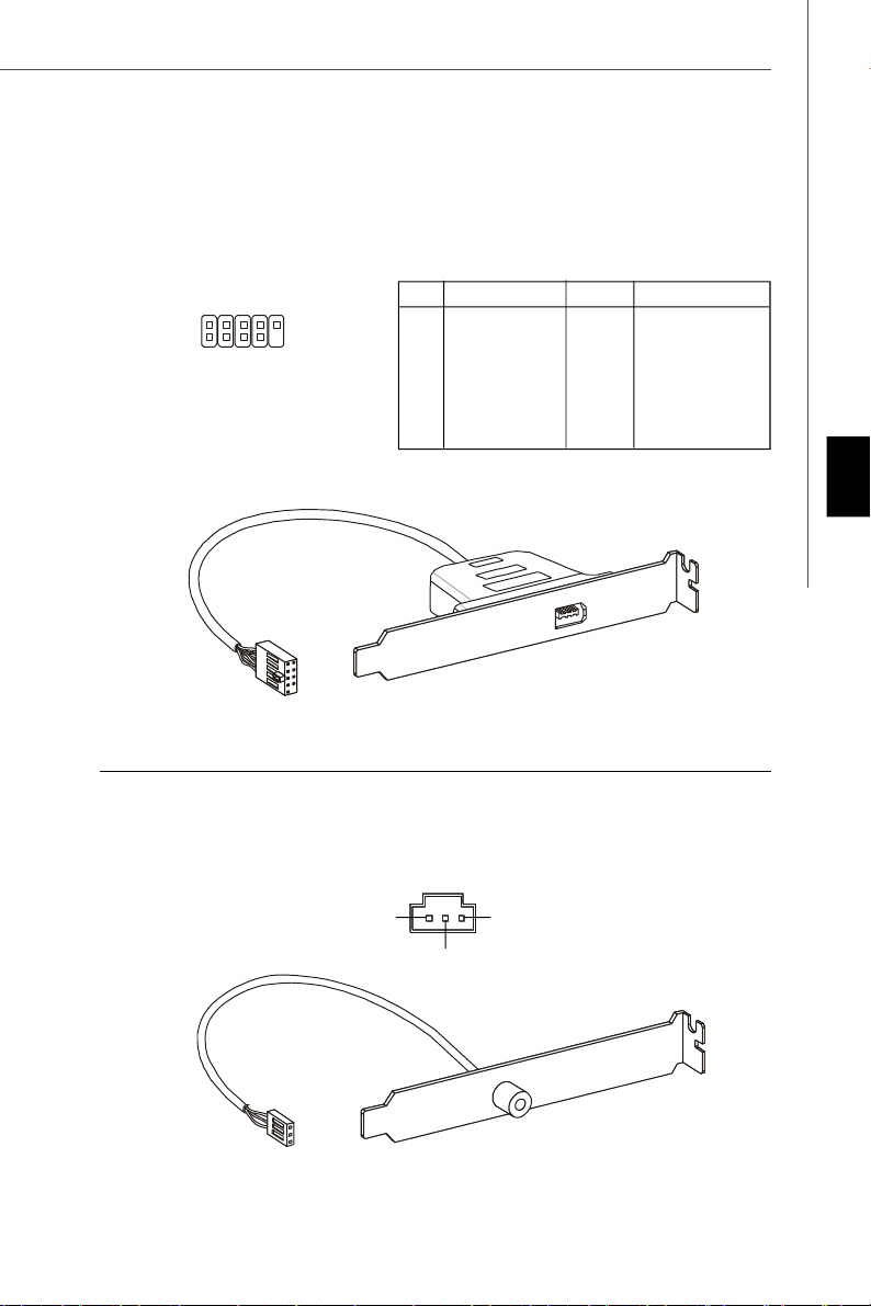
IEEE1394コネクター: J1394_1 (オプション)
このコネクターはオプションのIEEE1394ブラケット経由でIEEE1394デバイスを
接続します。
Pin Definition
PIN SIGNAL PIN SIGNAL
2
1
J1394_1
10
9
1 TPA+ 2 TPA-
3 Ground 4 Ground
5 TPB+ 6 TPB-
7 Cable power 8 Cable power
9 Key (no pin) 10 Ground
IEEE1394 Bracket
(オプション)
S/PDIF-Outコネクター: JSP1
デジタルフォーマットで音声ソースを出力するためのインターフェイスで
す。5.1チャンネル/7.1チャンネルサウンド音声に対応しています。
JSP1
日 本 語
VCC
GND
SPDIF
S/PDIF Bracket (オプション)
Jp-17
Page 100

MS-7514 マザーボード
フロントパネルコネルター: JFP1, JFP2
本製品にはフロントパネルスイッチやLEDを対象とした電子的接続用に、一つ
のフロントパネルコネクターが用意されています。JFP1はIntel® Front Panel I/
O Connectivity Design Guideに準拠しています。
JFP1 Pin Definition
PIN SIGNAL DESCRIPTION
1 HD_LED + Hard disk LED pull-up
2 FP PWR/SLP MSG LED pull-up
10
3 HD_LED - Hard disk active LED
9
4 FP PWR/SLP MSG LED pull-up
5 RST_SW - Reset Switch low reference pull-down to GND
6 PWR_SW + Power Switch high reference pull-up
7 RST_SW + Reset Switch high reference pull-up
8 PWR_SW - Power Switch low reference pull-down to GND
9 RSVD_DNU Reserved. Do not use.
JFP2 Pin Definition
PIN SIGNAL DESCRIPTION
1 GND Ground
2 SPK- Speaker-
8
7
3 SLED Suspend LED
4 BUZ+ Buzzer+
5 PLED Power LED
6 BUZ- Buzzer-
7 NC No connection
8 SPK+ Speaker+
JFP1
JFP2
Power
LED
2
1
2
1
+
- -
HDD
LED
Speaker
+
Power
LED
Power
Switch
-
+
+
Reset
Switch
+
-
CD-Inコネクター: JCD1
このコネクターはCD-ROMオーディオコネクターを接続します。
JCD1
R
L
GND
Jp-18
 Loading...