

Page 1
KA780GM Series
MS-7552 (V1.X) Mainboard
G52-75521X2
i
Page 2

Copyright Notice
The material in this document is the intellectual property of MICRO-STAR
INTERNATIONAL. We take every care in the preparation of this document, but no
guarantee is given as to the correctness of its contents. Our products are under
continual improvement and we reserve the right to make changes without notice.
Trademarks
All trademarks are the properties of their respective owners.
NVIDIA, the NVIDIA logo, DualNet, and nForce are registered trademarks or trade-
marks of NVIDIA Corporation in the United States and/or other countries.
AMD, Athlon™ , Athlon™ XP, Thoroughbred™, and Duron™ are registered trade-
marks of AMD Corporation.
Intel® and Pentium® are registered trademarks of Intel Corporation.
PS/2 and OS®/2 are registered trademarks of International Business Machines
Corporation.
Windows® 2000/NT/XP/Vista are registered trademarks of Microsoft Corporation.
Netware® is a registered trademark of Novell, Inc.
Award® is a registered trademark of Phoenix Technologies Ltd.
AMI® is a registered trademark of American Megatrends Inc.
Revision History
Revision Revision History Date
V1.0 First release for Asia September 2008
Technical Support
If a problem arises with your system and no solution can be obtained from the user’ s
manual, please contact your place of purchase or local distributor. Alternatively,
please try the following help resources for further guidance.
Visit the MSI website for FAQ, technical guide, BIOS updates, driver updates,
and other information: http://global.msi.com.tw/index.php?
func=service
Contact our technical staff at: http://ocss.msi.com.tw
ii
Page 3
Safety Instructions
1. Always read the safety instructions carefully.
2. Keep this User’s Manual for future reference.
3. Keep this equipment away from humidity.
4. Lay this equipment on a reliable flat surface before setting it up.
5. The openings on the enclosure are for air convection hence protects the equipment from overheating. DO NOT COVER THE OPENINGS.
6. Make sure the voltage of the power source and adjust properly 110/220V before connecting the equipment to the power inlet.
7. Place the power cord such a way that people can not step on it. Do not place
anything over the power cord.
8. Always Unplug the Power Cord before inserting any add-on card or module.
9. All cautions and warnings on the equipment should be noted.
10. Never pour any liquid into the opening that could damage or cause electrical
shock.
11. If any of the following situations arises, get the equipment checked by service
personnel:
† The power cord or plug is damaged.
† Liquid has penetrated into the equipment.
† The equipment has been exposed to moisture.
† The equipment does not work well or you can not get it work according to
User’s Manual.
† The equipment has dropped and damaged.
† The equipment has obvious sign of breakage.
12. DO NOT LEAVE THIS EQUIPMENT IN AN ENVIRONMENT UNCONDITIONED, STORAGE TEMPERATURE ABOVE 600 C (1400F), IT MAY DAMAGE THE EQUIPMENT.
CAUTION: Danger of explosion if battery is incorrectly replaced.
Replace only with the same or equivalent type recommended by the
manufacturer.
iii
Page 4
FCC-B Radio Frequency Interference Statement
This equipment has been
tested and found to comply
with the limits for a Class B
digital device, pursuant to Part
15 of the FCC Rules. These limits are designed to provide reasonable protection
against harmful interference in a residential installation. This equipment generates,
uses and can radiate radio frequency energy and, if not installed and used in accor-
dance with the instructions, may cause harmful interference to radio communications.
However, there is no guarantee that interference will not occur in a particular
installation. If this equipment does cause harmful interference to radio or television
reception, which can be determined by turning the equipment off and on, the user is
encouraged to try to correct the interference by one or more of the measures listed
below.
† Reorient or relocate the receiving antenna.
† Increase the separation between the equipment and receiver.
† Connect the equipment into an outlet on a circuit different from that to
which the receiver is connected.
† Consult the dealer or an experienced radio/television technician for help.
Notice 1
The changes or modifications not expressly approved by the party responsible for
compliance could void the user’s authority to operate the equipment.
Notice 2
Shielded interface cables and A.C. power cord, if any, must be used in order to
comply with the emission limits.
VOIR LA NOTICE D ’INSTALLATION AVANT DE RACCORDER AU RESEAU.
Micro-Star International
MS-7552
This device complies with Part 15 of the FCC Rules. Operation is subject to the
following two conditions:
(1) this device may not cause harmful interference, and
(2) this device must accept any interference received, including interference that
may cause undesired operation.
iv
Page 5
WEEE (Waste Electrical and Electronic Equipment) Statement
v
Page 6
vi
Page 7
vii
Page 8

CONTENTS
Copyright Notice.......................................................................................................ii
Trademarks..............................................................................................................ii
Revision History.......................................................................................................ii
Technical Support....................................................................................................ii
Safety Instructions...................................................................................................iii
FCC-B Radio Frequency Interference Statement...................................................iv
WEEE (Waste Electrical and Electronic Equipment) Statement............................v
English..............................................................................................En-1
Mainboard Specifications.........................................................................................En-2
Quick Components Guide........................................................................................En-4
CPU (Central Processing Unit)................................................................................En-5
Memory.....................................................................................................................En-8
Power Supply...........................................................................................................En-10
Back Panel...............................................................................................................En-11
Connectors...............................................................................................................En-13
Jumper......................................................................................................................En-21
Slots..........................................................................................................................En-22
BIOS Setup..............................................................................................................En-26
Software Information................................................................................................En-33
......................................................................................................................
한국어
메인보드 사양 ..........................................................................................................Kr-2
빠른 부품 설명서.....................................................................................................Kr-
CPU (중앙 처리 장치).............................................................................................Kr-5
메모리.......................................................................................................................Kr-8
전원 공급장치 ..........................................................................................................Kr-10
후면 패널..................................................................................................................Kr-11
커넥터.......................................................................................................................Kr-13
점퍼...........................................................................................................................Kr-21
슬롯...........................................................................................................................Kr-22
BIOS 설정................................................................................................................Kr-26
소프트웨어 정보.......................................................................................................Kr-33
Kr-1
4
日本語..................................................................................................................... Jp-1
マザーボードの仕様.................................................................................................Jp-2
viii
Page 9

クイックコンポーネントガイド..............................................................................Jp-4
CPU に関する注意事項...........................................................................................Jp-5
メモリ.......................................................................................................................Jp-8
電源 ..........................................................................................................................Jp-10
バックパネル............................................................................................................Jp-11
コネクター...............................................................................................................Jp-13
ジャンパ...................................................................................................................Jp-21
スロット...................................................................................................................Jp-22
BIOS の設定.............................................................................................................Jp-26
ソフトウェアの情報.................................................................................................Jp-33
繁體中文................................................................................... Tc-1
主機板規格.............................................................................................................Tc-2
快速安裝指南..........................................................................................................Tc-4
中央處理器..............................................................................................................Tc-5
記憶體......................................................................................................................Tc-8
電源供應器..............................................................................................................Tc-10
背板..........................................................................................................................Tc-11
連接器......................................................................................................................Tc-13
跳線..........................................................................................................................Tc-21
插槽..........................................................................................................................Tc-22
BIOS 設定................................................................................................................Tc-26
軟體訊息..................................................................................................................Tc-33
简体中文.............................................................................................Sc-1
主板规格....................................................................................................................Sc-2
组件指南....................................................................................................................Sc-4
中央处理器: CPU.......................................................................................................Sc-5
内存...........................................................................................................................Sc-8
电源适配器.................................................................................................................Sc-10
后置面板....................................................................................................................Sc-11
接口...........................................................................................................................Sc-13
跳线...........................................................................................................................Sc-21
插槽...........................................................................................................................Sc-22
BIOS 设置.................................................................................................................Sc-26
软件信息....................................................................................................................Sc-33
ix
Page 10

This page is intentionally left blank.
viii
Page 11

KA780GM Series
User’s Guide
Engli sh
English
En-1
Page 12
MS-7552 Mainboard
Mainboard Specifications
Processor Support
- Supports AMD® Athlon64 / Athlon64 X2 /AM2+ processors
- Supports 4 pin CPU Fan Pin-Header with Fan Speed Control
- Supports up to 5000+ and higher CPU
(For the latest information about CPU, please visit
http://global.msi.com.tw/index.php?func=cpuform)
HyperTransport
- Supports HyperTransport 3.0
Chipset
- North Bridge: AMD 780G
- South Birdge: AMD SB700
Memory Support
- DDR2 533/667/800/1066 SDRAM (240pin / 1.8V)
- 4 DDR2 DIMMs (16GB Max)
(For more information on compatible components, please visit
http://global.msi.com.tw/index.php?func=testreport)
Side Port Memory
- DDR3 SDRAM 1Gbit (optional)
LAN
- Supports LAN 10/100/1000 Fast Ethermet by RTL8111C
IEEE 1394
- Chip integrated by JMicron 381
- Transfer rate is up to 400Mb/s
Audio
- Chip integrated by Realtek® ALC888
- Flexible 8-channel audio with jack sensing
- Compliant with Azalia 1.0 Spec
IDE
- 1 IDE port by SB700
- Supports Ultra DMA 33/66/100/133 mode
- Supports PIO, Bus Master operation mode
SATA
- SATA II ports by SB700
- Supports 6 SATA II devices (included 1 eSATA )
- Supports storage and data transfers at up to 3 Gb/s
En-2
Page 13
Floppy
- 1 floppy port
- Supports 1 FDD with 360KB, 720KB, 1.2MB, 1.44MB and 2.88MB
RAID
- Supports RAID 0/ 1/ 0+1 mode by SB700
Connectors
Back panel
- 1 PS/2 mouse port
- 1 PS/2 keyboard port
- 1 VGA port
- 1 DVI port
- 1 HDMI port
- 1 Optical SPDIF jack
- 1 IEEE 1394 port
- 4 USB 2.0 ports
- 1 eSATA port
- 1 LAN jack
- 6 flexible audio jacks
On-Board Pinheaders/ Connectors
- 4 USB 2.0 pinheaders
- 1 COM port pinheader
- 1 CD-In connector
- 1 Front Panel Audio pinheader
- 1 IEEE 1394 pinheader
- 1 Chassis Intrusion Switch pinheader
- 1 TPM Module pinheader
- 1 JLPT pinheader
Slots
- 1 PCI Express x16 slot
- 1 PCI Express x1 slot
- 2 PCI slots
Form Factor
- M-ATX (24.4cm X 24.4 cm)
Mounting
- 6 mounting holes
Engli sh
En-3
Page 14
MS-7552 Mainboard
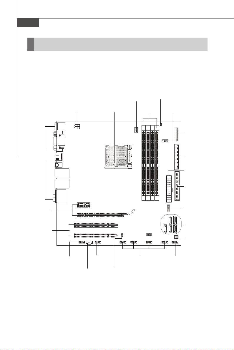
Quick Components Guide
Back Panel,
En-11
PCIE,
En-22
PCI,
En-23
JPWR2,
En-10
JAUD1,
En-17
JCD1,
En-17
J1394_1,
En-20
CPU,
En-5
JBAT1,
En-21
CPUFAN1
En-15
DDR2,
En-8
JUSB1~4,
En-19
JCI1,
En-15
JCOM1,
En-16
JLPT1,
En-18
FDD1,
En-13
JPWR1,
En-10
IDE1,
En-13
JTPM1,
En-16
SATA1~5,
En-14
SYSFAN1,
En-15
JFP1,
En-18
En-4
Page 15
CPU (Central Processing Unit)
When you are installing the CPU, make sure to install the cooler to prevent
overheating. If you do not have the CPU cooler, consult your dealer before turning
on the computer.
For the latest information about CPU, please visit http://global.msi.com.tw/index.php?
func=cpuform
Important
Overheating
Overheating will seriously damage the CPU and system. Always make sure
the cooling fan can work properly to protect the CPU from overheating. Make
sure that you apply an even layer of thermal paste (or thermal tape) between
the CPU and the heatsink to enhance heat dissipation.
Replaceing the CPU
While replacing the CPU, always turn off the ATX power supply or unplug the
power supply’s power cord from the grounded outlet first to ensure the safety
of CPU.
Overclocking
This mainboard is designed to support overclocking. However, please make
sure your components are able to tolerate such abnormal setting, while
doing overclocking. Any attempt to operate beyond product specifications is
not recommended. We do not guarantee the damages or risks caused
by inadequate operation or beyond product specifications.
Engli sh
En-5
Page 16
MS-7552 Mainboard
Gold arrow
Gold arrow
Gold arrow
Correct CPU placement
O
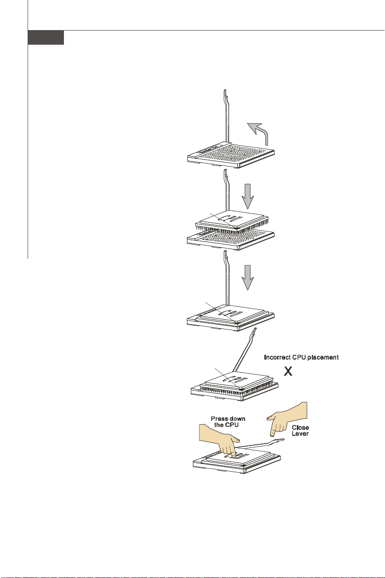
CPU Installation Procedures for Socket AM2+
1.Please turn off the power and
unplug the power cord before
installing the CPU.
2.Pull the lever sideways away
from the socket. Make sure to
raise the lever up to a 90-degree angle.
3.Look for the gold arrow of the
CPU. The gold arrow should
point as shown in the picture.
The CPU can only fit in the correct orientation.
4.If the CPU is correctly installed,
the pins should be completely
embedded into the socket and
can not be seen. Please note
that any violation of the correct
installation procedures may
cause permanent damages to
your mainboard.
Sliding
Plate
Open Lever
90 degree
5. Press the CPU down firmly into
the socket and close the lever.
As the CPU is likely to move while
the lever is being closed, always close the lever with your
fingers pressing tightly on top of
the CPU to make sure the CPU is
properly and completely embedded into the socket.
En-6
Page 17
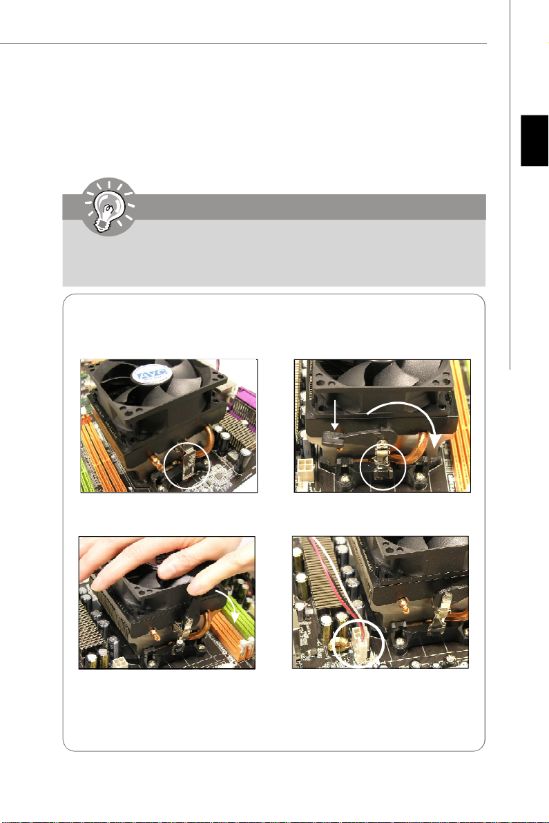
Installing AMD Socket AM2+ CPU Cooler Set
When you are installing the CPU, make sure the CPU has a heat sink and a
cooling fan attached on the top to prevent overheating. If you do not have the
heat sink and cooling fan, contact your dealer to purchase and install them before
turning on the computer.
Important
Mainboard photos shown in this section are for demonstration of the cooler
installation for Socket AM2+ CPUs only. The appearance of your mainboard
may vary depending on the model you purchase.
Engli sh
1.Position the cooling set onto the retention mechanism.
Hook one end of the clip to hook
first.
3.Fasten down the lever.
* While disconnecting the Safety Hook from the fixed bolt, it is necessary to
keep an eye on your fingers, because once the Safety Hook is disconnected
from the fixed bolt, the fixed lever will spring back instantly.
2. Then press down the other end of
the clip to fasten the cooling set on
the top of the retention mechanism.
Locate the Fix Lever and lift up it .
Fixed Lever
4.Attach the CPU Fan cable to the CPU
fan connector on the mainboard.
En-7
Page 18
MS-7552 Mainboard
1
2
3
Installed
Memory
These DIMM slots are used for installing memory modules.
For more information on compatible components, please visit http://global.msi.com.
tw/index.php?func=testreport
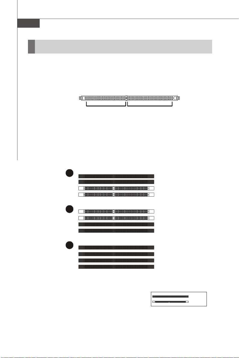
DDR2
240-pin, 1.8V
64x2=128 pin56x2=112 pin
Dual-Channel Memory Population Rules
In Dual-Channel mode, the memory modules can transmit and receive data with two
data bus lines simultaneously. Enabling Dual-Channel mode can enhance the system
performance. Please refer to the following illustrations for population rules under
Dual-Channel mode.
DIMM1
DIMM2
DIMM3
DIMM4
DIMM1
DIMM2
DIMM3
DIMM4
DIMM1
DIMM2
DIMM3
DIMM4
Empty
En-8
Page 19
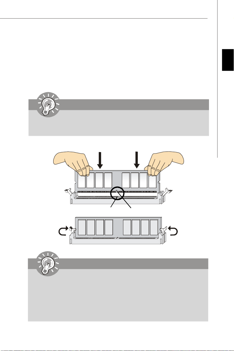
Installing Memory Modules
1. The memory module has only one notch on the center and will only fit in the right
orientation.
2. Insert the memory module vertically into the DIMM slot. Then push it in until the
golden finger on the memory module is deeply inserted in the DIMM slot. The plastic
clip at each side of the DIMM slot will automatically close when the memory module
is properly seated.
Important
You can barely see the golden finger if the memory module is properly inserted
in the DIMM slot.
3. Manually check if the memory module has been locked in place by the DIMM slot
clips at the sides.
Engli sh
Volt
Notch
Important
-DDR2 memory modules are not interchangeable with DDR and the DDR2
standard is not backwards compatible. You should always install DDR2
memory modules in the DDR2 DIMM slots.
-In Dual-Channel mode, make sure that you install memory modules of the
same type and density in different channel DIMM slots.
-To enable successful system boot-up, always insert the memory modules
into the DIMM1 first.
En-9
Page 20
MS-7552 Mainboard
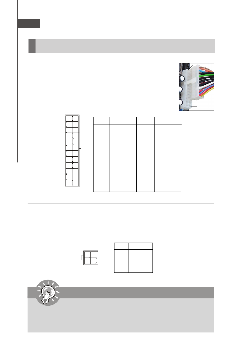
Power Supply
ATX 24-Pin Power Connector: JPWR1
This connector allows you to connect an ATX 24-pin power supply.
To connect the ATX 24-pin power supply, make sure the plug of the
power supply is inserted in the proper orientation and the pins are
aligned. Then push down the power supply firmly into the connector.
You may use the 20-pin ATX power supply as you like. If you’d like
to use the 20-pin ATX power supply, please plug your power supply along with pin 1 & pin 13 (refer to the image at the right hand).
Pin Definition
PIN SIGNAL
13 +3.3V
14 -12V
15 GND
16 PS-ON#
17 GND
18 GND
19 GND
20 Res
21 +5V
22 +5V
23 +5V
24 GND
JPWR1
12
1
24
13
PIN SIGNAL
1 +3.3V
2 +3.3V
3 GND
4 +5V
5 GND
6 +5V
7 GND
8 PWR OK
9 5VSB
10 +12V
11 +12V
12 +3.3V
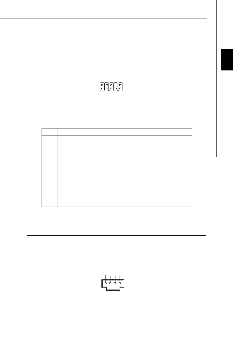
ATX 4-Pin Power Connector: JPWR2
This 12V power connector JPW1 is used to provide power to the CPU.
pin 13
pin 12
JPWR2
4
3
2
1
PIN SIGNAL
1 GND
2 GND
3 12V
4 12V
Important
1. Maker sure that all the connectors are connected to proper ATX power supplies to ensure stable operation of the mainboard.
2. Power supply of 450 watts (and above) is highly recommended for system
stability.
En-10
Pin Definition
Page 21
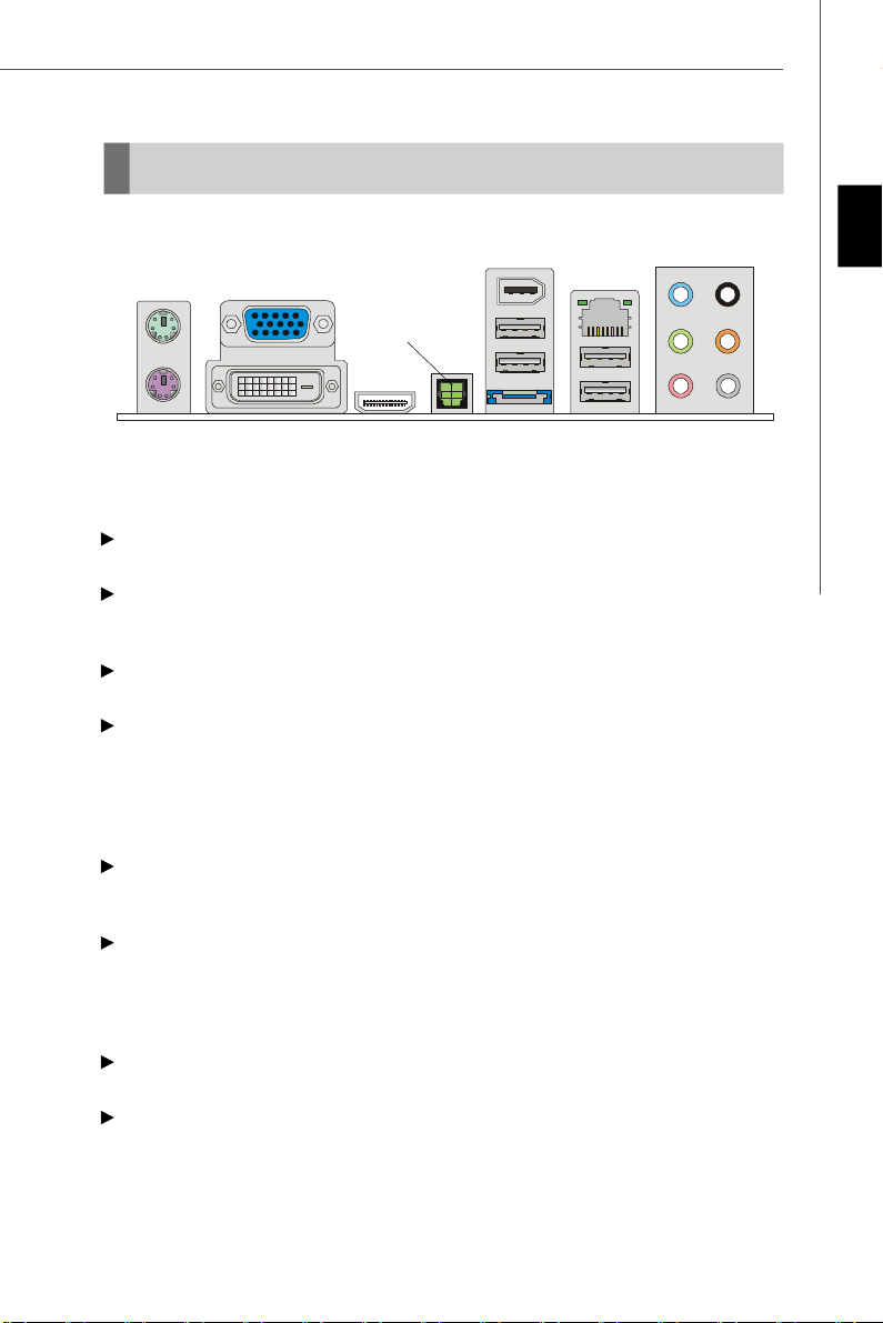
Back Panel
1394 Port
Keyboard
Mouse
VGA Port
DVI-D Port
Optical
S/PDIF-Out
HDMI Port
USB Ports
LAN
Line-Out
USB Ports
Line-In
Mic
RS-Out
CS-Out
SS-Out
eSATA Port
Keyboard / Mouse
The standard PS/2® keyboard / mouse DIN connector is for a PS/2® keyboard / mouse.
USB Port
The USB (Universal Serial Bus) port is for attaching USB devices such as keyboard,
mouse, or other USB-compatible devices.
VGA Port
The DB15-pin female connector is provided for monitor.
DVI-D Port
The DVI-D (Digital Visual Interface-Digital) connector allows you to connect a LCD
monitor. It provides a high-speed digital interconnection between the computer and
its display device. To connect an LCD monitor, simply plug your monitor cable into the
DVI connector, and make sure that the other end of the cable is properly connected
to your monitor (refer to your monitor manual for more information.)
Optical S/PDIF-Out
This SPDIF (Sony & Philips Digital Interconnect Format) connector is provided for
digital audio transmission to external speakers through an optical fiber cable.
HDMI Port
The High-Definition Multimedia Interface (HDMI) is an all-digital audio/video interface
capable of transmitting uncompressed streams. HDMI supports all TV format, including standard, enhanced, or high-definition video, plus multi-channel digital audio on a
single cable.
1394 Port
The IEEE1394 port on the back panel provides connection to IEEE1394 devices.
eSATA Port
The eSATA port is for attaching the eSATA external hard drive.
English
En-11
Page 22
MS-7552 Mainboard
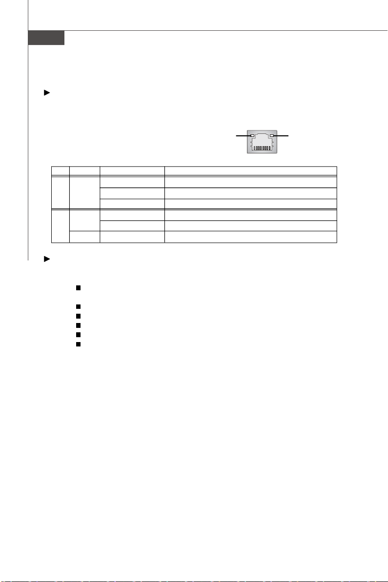
LAN
The standard RJ-45 LAN jack is for connection to the Local Area Network (LAN). You
can connect a network cable to it.
Green / OrangeYellow
LED Color LED State Condition
Off LAN link is not established.
Left Yellow On (steady state) LAN link is established.
On (brighter & pulsing)The computer is communicating with another computer on the LAN.
Green Off 10 Mbit/sec data rate is selected.
Right On 100 Mbit/sec data rate is selected.
Orange On 1000 Mbit/sec data rate is selected.
Audio Ports
These audio connectors are used for audio devices. You can differentiate the color
of the audio jacks for different audio sound effects.
Line-In (Blue) - Line In is used for external CD player, tapeplayer or
other audio devices.
Line-Out (Green) - Line Out, is a connector for speakers or headphones.
Mic (Pink) - Mic, is a connector for microphones.
RS-Out (Black) - Rear-Surround Out in 4/ 5.1/ 7.1 channel mode.
CS-Out (Orange) - Center/ Subwoofer Out in 5.1/ 7.1 channel mode.
SS-Out (Gray) - Side-Surround Out 7.1 channel mode.
En-12
Page 23
Connectors
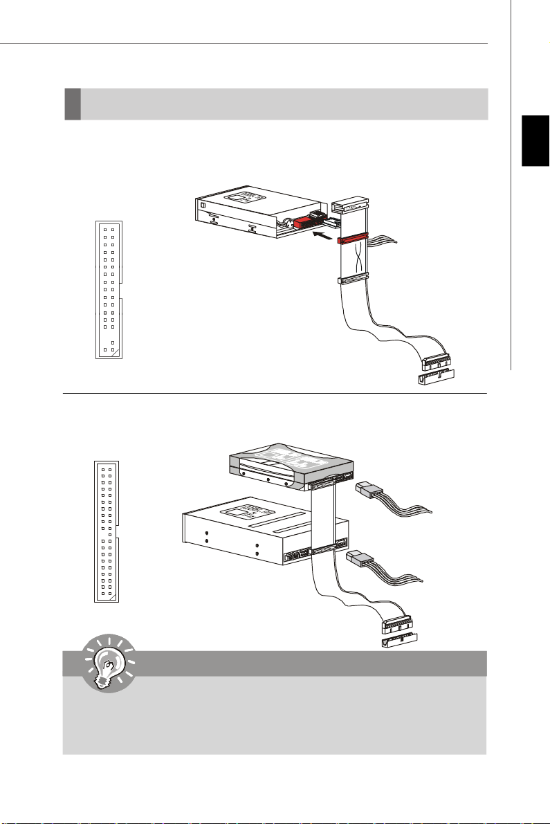
Floppy Disk Drive Connector: FDD1
This connector supports 360KB, 720KB, 1.2MB, 1.44MB or 2.88MB floppy disk drive.
FDD1
IDE Connector: IDE1
This connector supports IDE hard disk drives, optical disk drives and other IDE devices.
IDE1
English
Important
If you install two IDE devices on the same cable, you must configure the
drives separately to master / slave mode by setting jumpers. Refer to IDE
device’s documentation supplied by the vendors for jumper setting
instructions.
En-13
Page 24
MS-7552 Mainboard
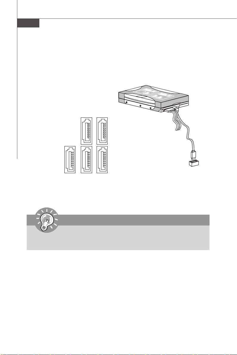
Serial ATA Connector: SATA1~ SATA5
This connector is a high-speed Serial ATA interface port. Each connector can connect
to one Serial ATA device.
SATA4
SATA1
SATA2
SATA5
SATA3
Important
Please do not fold the Serial ATA cable into 90-degree angle. Otherwise,
data loss may occur during transmission.
En-14
Page 25
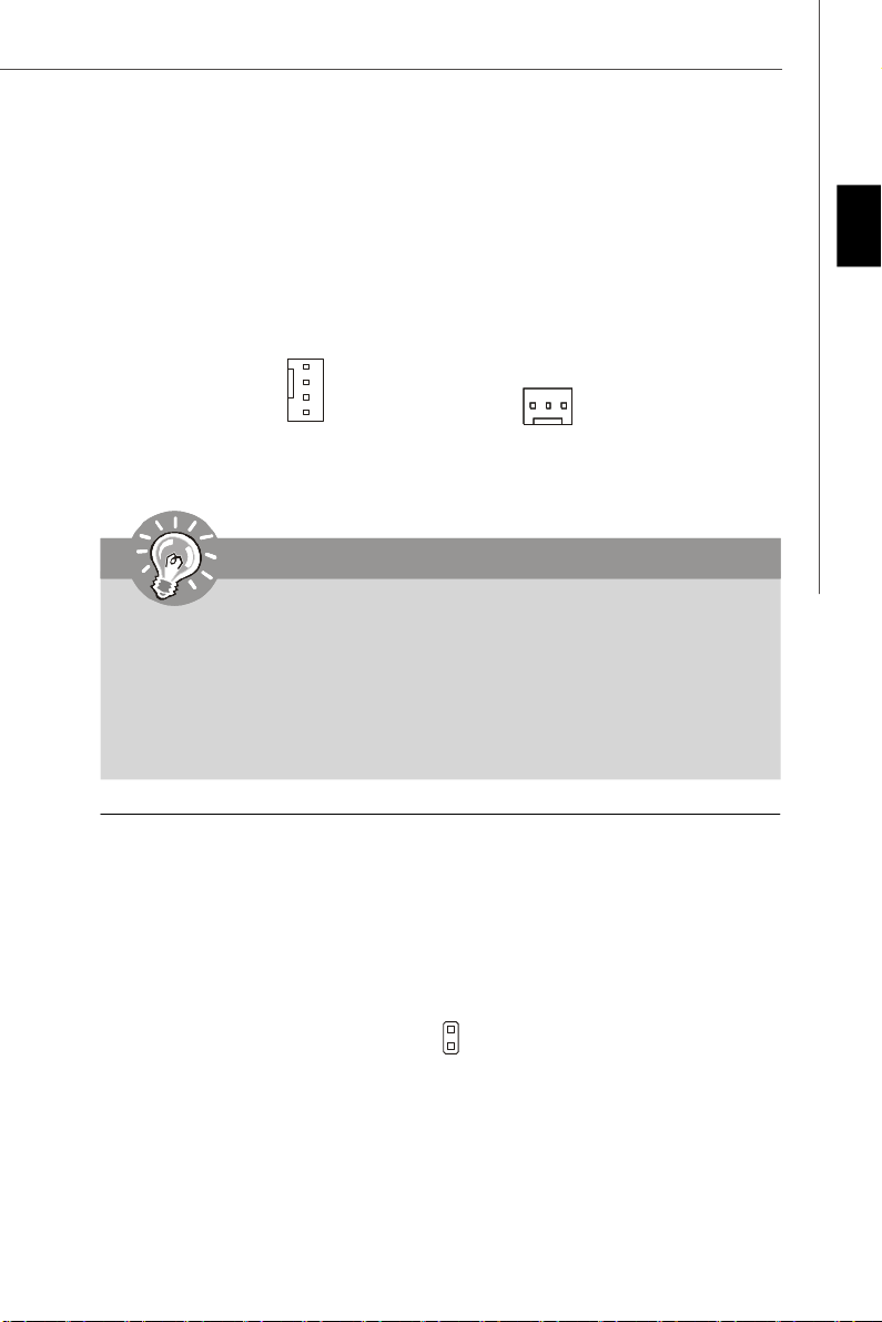
Fan Power Connectors: CPUFAN1, SYSFAN1
The fan power connectors support system cooling fan with +12V. When connecting
the wire to the connectors, always note that the red wire is the positive and should
be connected to the +12V; the black wire is Ground and should be connected to GND.
If the mainboard has a System Hardware Monitor chipset on-board, you must use a
specially designed fan with speed sensor to take advantage of the CPU fan control.
English
GND
+12V
SENSOR
Control
CPUFAN1
+1 2V
SE NS OR
GND
SYSFAN1
Important
1.Please refer to the recommended CPU fans at processor’s official website
or consult the vendors for proper CPU cooling fan.
2.CPUFAN1 supports fan control. You can install Dual Core Center utility
that will automatically control the CPU fan speed according to the actual
CPU temperature.
3. Fan cooler set with 3 or 4 pins power connector are both available for
CPUFAN1.
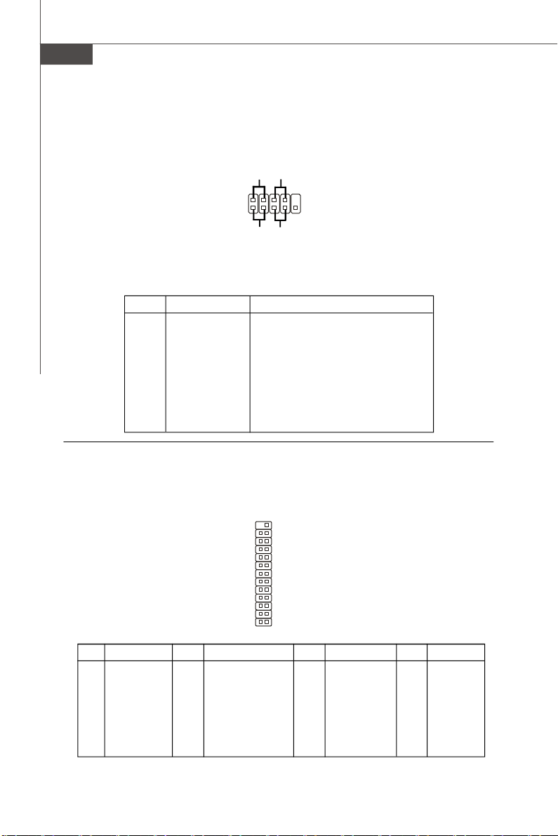
Chassis Intrusion Connector: JCI1
This connector connects to the chassis intrusion switch cable. If the chassis is
opened, the chassis intrusion mechanism will be activated. The system will record
this status and show a warning message on the screen. To clear the warning, you
must enter the BIOS utility and clear the record.
GND
CINTRU
JCI1
2
1
En-15
Page 26
MS-7552 Mainboard
TPM Module Connector: JTPM1
This connector connects to a TPM (Trusted Platform Module) module (optional). Please
refer to the TPM security platform manual for more details and usages.
13
14
2 1
JTPM1
Pin Signal Description Pin Signal Description
1 LCLK LPC clock 2 3V_STB 3V standby power
3 LRST# LPC reset 4 VCC3 3.3V power
5 LAD0 LPC address & data pin0 6 SIRQ Serial IRQ
7 LAD1 LPC address & data pin1 8 VCC5 5V power
9 LAD2 LPC address & data pin2 10 KEY No pin
11 LAD3 LPC address & data pin3 12 GND Ground
13 LFRAME# LPC Frame 14 GND Ground
Serial Port Connector: JCOM 1
This connector is a 16550A high speed communication port that sends/receives 16
bytes FIFOs. You can attach a serial device.
Pin Definition
PIN SIGNAL DESCRIPTION
1 DCD Data Carry Detect
2 SIN Serial In or Receive Data
3 SOUT Serial Out or Transmit Data
4 DTR Data Terminal Ready
5 GND Ground
6 DSR Data Set Ready
7 RTS Request To Send
8 CTS Clear To Send
9 RI Ring Indicate
En-16
JCOM1
9
1
2
Page 27
Front Panel Audio Connector: JAUD1
This connector allows you to connect the front panel audio and is compliant with
Intel® Front Panel I/O Connectivity Design Guide.
English
2
1
10
9
JAUD1
HD Audio Pin Definition
PIN SIGNAL DESCRIPTION
1 MIC_L Microphone - Left channel
2 GND Ground
3 MIC_R Microphone - Right channel
4 PRESENCE# Active low signal-signals BIOS that a High Definition Audio dongle
5 LINE out_R Analog Port - Right channel
6 MIC_JD Jack detection return from front panel microphone JACK1
7 Front_JD Jack detection sense line from the High Definition Audio CODEC
8 NC No control
9 LINE out_L Analog Port - Left channel
10 LINEout_JD Jack detection return from front panel JACK2
is connected to the analog header. PRESENCE# = 0 when a
High Definition Audio dongle is connected
jack detection resistor network
CD-In Connector: JCD1
This connector is provided for external audio input.
JCD1
GND
R L
En-17
Page 28
MS-7552 Mainboard
Front Panel Connector: JFP1
These connectors are for electrical connection to the front panel switches and LEDs.
The JFP1 is compliant with Intel® Front Panel I/O Connectivity Design Guide.
Power
Power
LED
Switch
-
+
2
JFP1
1
+
HDD
LED
JFP1 Pin Definition
PIN SIGNAL DESCRIPTION
1 HD_LED + Hard disk LED pull-up
2 FP PWR/SLP MSG LED pull-up
3 HD_LED - Hard disk active LED
4 FP PWR/SLP MSG LED pull-up
5 RST_SW - Reset Switch low reference pull-down to GND
6 PWR_SW + Power Switch high reference pull-up
7 RST_SW + Reset Switch high reference pull-up
8 PWR_SW - Power Switch low reference pull-down to GND
9 RSVD_DNU Reserved. Do not use.
-
-
+
Reset
Switch
10
9
Parallel Port Header: JLPT1
This connector is used to connect an optional parallel port bracket. The parallel port
is a standard printer port that supports Enhanced Parallel Port (EPP) and Extended
Capabilities Parallel Port (ECP) mode.
PIN SIGNAL PIN SIGNAL
1 RSTB# 2 AFD#
3 PRND0 4 ERR#
5 PRND1 6 PINIT#
7 PRND2 8 LPT_SLIN#
9 PRND3 10 GND
11 PRND4 12 GND
13 PRND5 14 GND
En-18
JLPT1
26 25
2
1
PIN SIGNAL PIN SIGNAL
15 PRND6 16 GND
17 PRND7 18 GND
19 ACK# 20 GND
21 BUSY 22 GND
23 PE 24 GND
25 SLCT 26 Key (No Pin)
Page 29
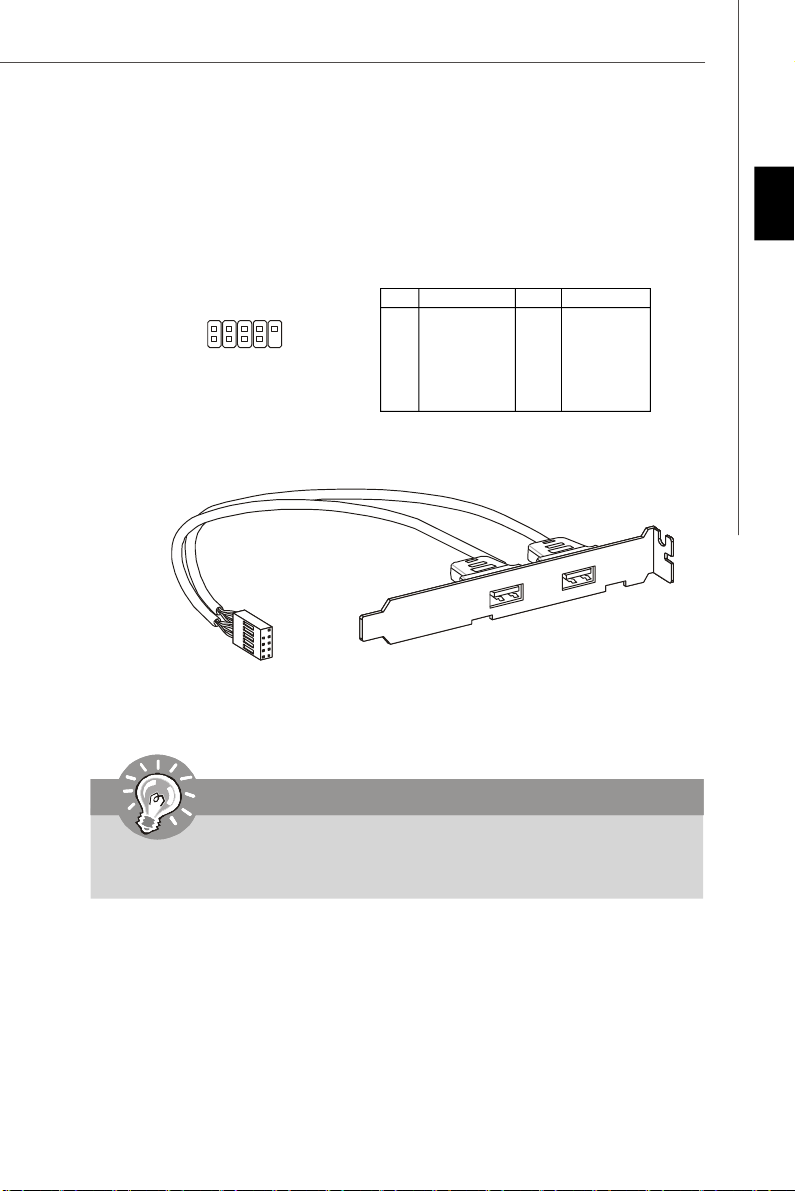
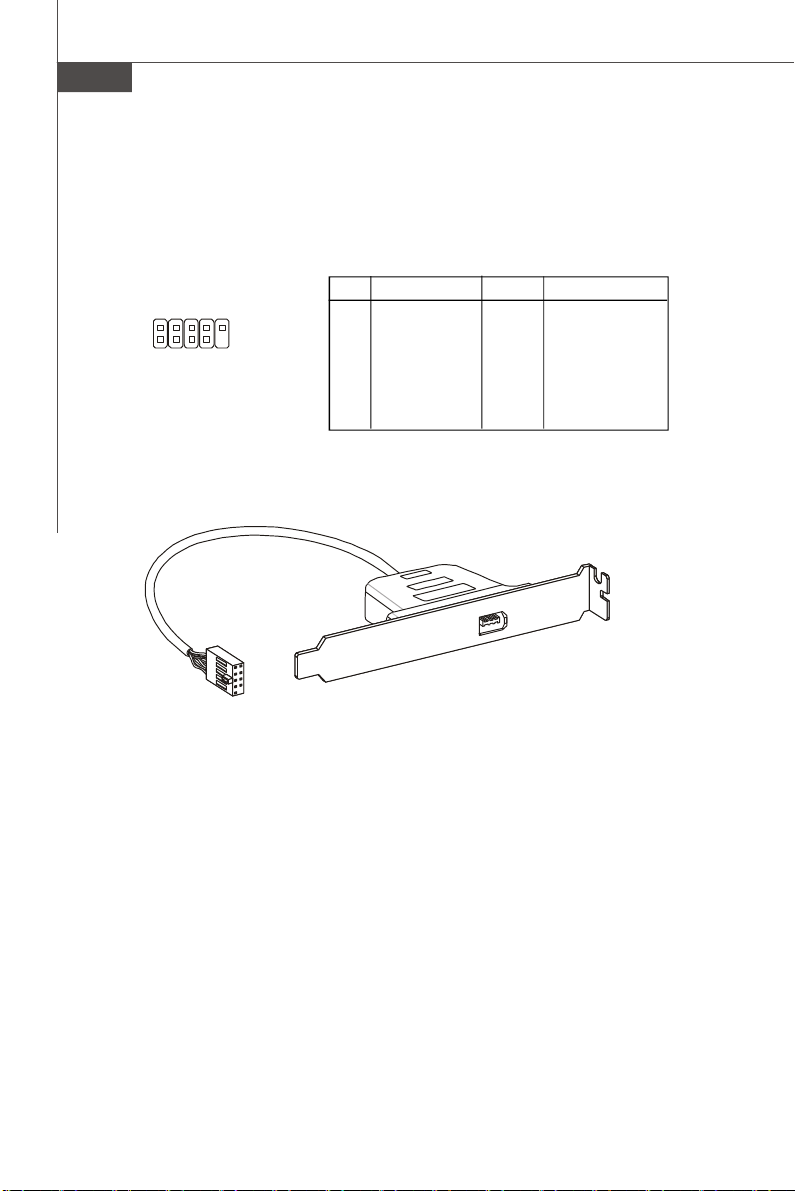
Front USB Connector: JUSB1 ~ 4
These connectors, compliant with Intel® I/O Connectivity Design Guide, is ideal for
connecting high-speed USB interface peripherals such as USB HDD, digital cameras,
MP3 players, printers, modems and the like.
Pin Definition
JUSB1~4
2
1
10
9
PIN SIGNAL PIN SIGNAL
1 VCC 2 VCC
3 USB0- 4 USB1-
5 USB0+ 6 USB1+
7 GND 8 GND
9 Key (no pin) 10 USBOC
USB 2.0 Bracket
(Optional)
English
Important
Note that the pins of VCC and GND must be connected correctly to avoid
possible damage.
En-19
Page 30
MS-7552 Mainboard
IEEE1394 Connector: J1394_1
This connector allows you to connect the IEEE1394 device via an optional IEEE1394
bracket.
Pin Definition
PIN SIGNAL PIN SIGNAL
2
1
J1394_1
9
10
1 TPA+ 2 TPA-
3 Ground 4 Ground
5 TPB+ 6 TPB-
7 Cable power 8 Cable power
9 Key (no pin) 10 Ground
En-20
IEEE1394 Bracket (Optional)
Page 31

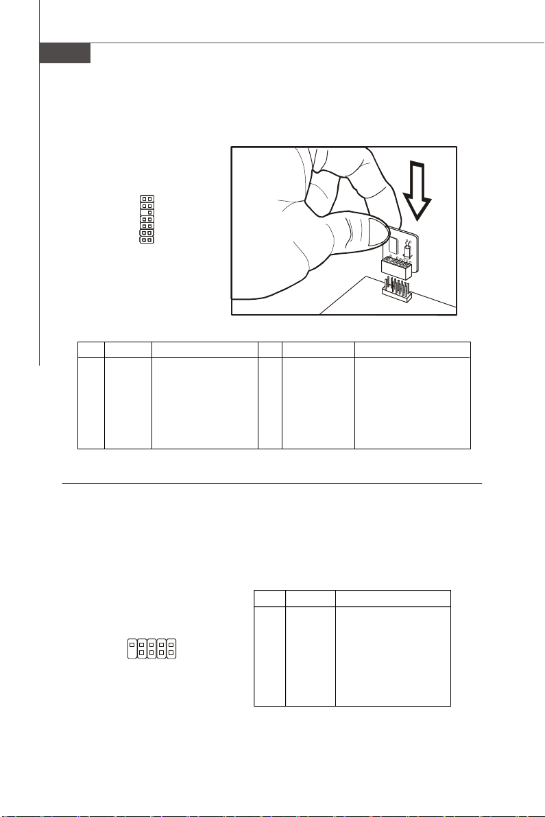
Jumpers
Clear CMOS Jumper: JBAT1
There is a CMOS RAM onboard that has a power supply from an external battery to
keep the data of system configuration. With the CMOS RAM, the system can automatically boot OS every time it is turned on. If you want to clear the system configuration,
set the jumper to clear data.
1
JBAT1
1
3
Keep Data
1
3
Clear Data
Important
You can clear CMOS by shorting 2-3 pin while the system is off. Then return
to 1-2 pin position. Avoid clearing the CMOS while the system is on; it will
damage the mainboard.
English
En-21
Page 32

MS-7552 Mainboard
Slots
PCI (Peripheral Component Interconnect) Express Slot
The PCI Express slot supports the PCI Express interface expansion card.
The PCI Express 2.0 x16 supports up to 8 GB/s transfer rate.
The PCI Express x1 supports up to 250 MB/s transfer rate.
PCI Express 2.0 x16 Slot
PCI Express x 1 Slot
Important
When adding or removing expansion cards, make sure that you unplug the
power supply first. Meanwhile, read the documentation for the expansion
card to configure any necessary hardware or software settings for the expansion card, such as jumpers, switches or BIOS configuration.
En-22
Page 33

PCI (Peripheral Component Interconnect) Slot
The PCI slot supports LAN card, SCSI card, USB card, and other add-on cards that
comply with PCI specifications.
32-bit PCI Slot
Important
When adding or removing expansion cards, make sure that you unplug the
power supply first. Meanwhile, read the documentation for the expansion card
to configure any necessary hardware or software settings for the expansion
card, such as jumpers, switches or BIOS configuration.
PCI Interrupt Request Routing
The IRQ, acronym of interrupt request line and pronounced I-R-Q, are hardware lines
over which devices can send interrupt signals to the microprocessor. The PCI IRQ
pins are typically connected to the PCI bus pins as follows:
English
Order 1 Order 2 Order 3 Order 4
PCI Slot 1 INT A# INT B# INT C# INT D#
PCI Slot 2 INT B# INT C# INT D# INT A#
En-23
Page 34

MS-7552 Mainboard
Hybrid CrossFireTM Technology
Hybrid CrossFireXTM technology brings multi-GPU performance capabilities by enabling an AMD 780 integrated graphics processor and a discrete graphics processor
to operate simultaneously with combined output to a single display for blisteringlyfast frame rates. Unleash the graphics performance.
System Request
1. Hybrid CrossFireXTM is only supported with the Vista operating system.
2. Graphic card based on an ATI RadeonTM HD 2400 Series2, ATI RadeonTM HD 3400
Series or ATI Mobility RadeonTM HD 3400 Series graphics processor.
3. Mainboard based on an AMD 780 integrated chipset.
Enabling Hybrid CrossFireTM Technology
Power off the system and install the ATI graphic card that supports Hybrid CrossFireX
technology. After then, power on the system and install the driver that Hybrid
CrossFireX technology. Restart the system and wait for the ATI Icon to show in the
System Tray. Click the icon and then the following aspect appears in Catalyst™
Control Center:
1. Select the Advanced View from the
view drop menu.
En-24
Page 35

2. From the Graphics Settings tree in the CatalystTM Control Center, click CrossFireTM.
3. From the Graphics Adapter list, select the graphics card that acts as the Display
GPU.
4. Select Enable CrossFire
TM
5. Click Apply.
When Hybrid CrossFireX is enabled, GPU Accelerated Physics is automatically disabled for all cards in the configuration as are all displays except the one used by
Hybrid CrossFireX.
More details please refer to http://game.amd.com/us-en/crossfirex_hybrid.aspx
Important
Changing integrated graphic memory operating mode may cause Hybrid
CrossFire fail. To avoid the issue, please follow the steps below to setup
the system:
1.Disable the Hybrid CrossFire in Catalyst Control Center.
2.Reboot and into BIOS
3.Select the option in Advanced BIOS Features -> Chipset Feature ->
On-Chip VGA
4.Save BIOS settings and reboot
5.Enable the Hybrid CrossFire in Catalyst Control Center.
English
En-25
Page 36

MS-7552 Mainboard
BIOS Setup
This chapter provides basic information on the BIOS Setup program and allows you to
configure the system for optimum use. You may need to run the Setup program
when:
* An error message appears on the screen during the system booting up, and requests you to run BIOS SETUP.
* You want to change the default settings for customized features.
Important
1.The items under each BIOS category described in this chapter are under
continuous update for better system performance. Therefore, the description
may be slightly different from the latest BIOS and should be held for reference
only.
2.Upon boot-up, the 1st line appearing after the memory count is the BIOS
version. It is usually in the format:
1st digit refers to BIOS maker as A = AMI, W = AWARD, and P = PHOENIX.
2nd - 5th digit refers to the model number.
6th refers to the Chipset vender as A = AMD, I = Intel, V = VIA, N = Nvidia, U =
ULi.
7th - 8th digit refers to the customer as MS = all standard customers.
V1.1 refers to the BIOS version.
082208 refers to the date this BIOS was released.
A7552AMS V1.0 082208 where:
En-26
Page 37

Entering Setup
Power on the computer and the system will start POST (Power On Self Test) process.
When the message below appears on the screen, press <DEL> key to enter Setup.
Press DEL to enter SETUP
If the message disappears before you respond and you still wish to enter Setup,
restart the system by turning it OFF and On or pressing the RESET button. You may
also restart the system by simultaneously pressing <Ctrl>, <Alt>, and <Delete> keys.
Getting Help
After entering the Setup menu, the first menu you will see is the Main Menu.
Main Menu
The main menu lists the setup functions you can make changes to. You can use the
arrow keys (↑↓ ) to select the item. The on-line description of the highlighted setup
function is displayed at the bottom of the screen.
Sub-Menu
If you find a right pointer symbol (as shown in the right view)
appears to the left of certain fields that means a sub-menu
containing additional options can be launched from this field.
You can use control keys (↑↓ ) to highlight the field and
press <Enter> to call up the sub-menu. Then you can use the control keys to enter
values and move from field to field within a sub-menu. If you want to return to the
main menu, just press <Esc >.
General Help <F1>
The BIOS setup program provides a General Help screen. You can call up this screen
from any menu by simply pressing <F1>. The Help screen lists the appropriate keys
to use and the possible selections for the highlighted item. Press <Esc> to exit the
Help screen.
English
En-27
Page 38

MS-7552 Mainboard
The Main Menu
Once you enter AMI® or AWARD® BIOS CMOS Setup Utility, the Main Menu will appear
on the screen. The Main Menu allows you to select from ten setup functions and two
exit choices. Use arrow keys to select among the items and press <Enter> to accept
or enter the sub-menu.
Standard CMOS Features
Use this menu for basic system configurations, such as time, date etc.
Advanced BIOS Features
Use this menu to setup the items of special enhanced features.
Integrated Peripherals
Use this menu to specify your settings for integrated peripherals.
Power Management Setup
Use this menu to specify your settings for power management.
H/W Monitor
This entry shows your PC health status.
BIOS Setting Password
Use this menu to set the Password.
Cell Menu
Use this menu to specify your settings for frequency/voltage control and overclocking.
Load Fail-Safe Defaults
Use this menu to load the default values set by the BIOS vendor for stable system
performance.
Load Optimized Defaults
Use this menu to load the default values set by the mainboard manufacturer specifically for optimal performance of the mainboard.
Save & Exit Setup
Save changes to CMOS and exit setup.
Exit Without Saving
Abandon all changes and exit setup.
En-28
Page 39

When enter the BIOS Setup utility, follow the processes below for general use.
1. Load Optimized Defaults : Use control keys (↑↓) to highlight the Load Opti-
mized Defaults field and press <Enter> , a message as below appears:
Select [Ok] and press Enter to load the default settings for optimal system
performance.
2. Setup Date/ Time : Select the Standard CMOS Features and press <Enter> to
enter the Standard CMOS Features-menu. Adjust the Date, Time fields.
3. Save & Exit Setup : Use control keys (↑↓) to highlight the Save & Exit Setup
field and press <Enter> , a message as below appears:
English
Select [Ok] and press Enter to save the configurations and exit BIOS Setup utility.
Important
The configuration above are for general use only. If you need the detailed
settings of BIOS, please see the manual in English version on MSI website.
En-29
Page 40

MS-7552 Mainboard
4. Cell Menu Introduction : This menu is for advanced user who want to overclock
the mainboard.
Important
Change these settings only if you are familiar with the chipset.
Current CPU / DRAM Frequency
These items show the current clocks of CPU and Memory speed. Read-only.
AMD Cool’n’Quiet
The Cool’ n’ Quiet technology can effectively and dynamically lower CPU speed and
power consumption.
En-30
Page 41

Important
To ensure that Cool’n’Quiet function is activated and will be working properly, it is
required to double confirm that:
1.Run BIOS Setup, and select Cell Menu.
Under Cell Menu, find AMD
Cool’n’Quiet, and set this item to
“Enable.”
2.Enter Windows, and select [Start]->
[Settings]->[Control Pannel]->[Power
Options]. Enter Power Options Prop-
erties tag, and select Minimal Power
Management under Power schemes.
Adjust CPU FSB Frequency (MHz)
This item allows you to adjust the CPU FSB frequency.
Adjust CPU Ratio
This item lets you to adjust the CPU ratio. It is available only when the processor
supports this function.
Adjusted CPU Frequency (MHz)
It shows the adjusted CPU frequency (FSB x Ratio). Read-only.
Advance DRAM Configuration
Press <Enter> to enter the sub-menu and the following screen appears.
English
DRAM Timing Mode
Setting to [Auto] enables DRAM CAS# Latency automatically to be determined by
BIOS based on the configurations on the SPD (Serial Presence Detect) EEPROM
on the DRAM module.
1T/2T Memory Timing
This field controls the SDRAM command rate. Selecting [1T] makes SDRAM
signal controller to run at 1T (T=clock cycles) rate. Selecting [2T] makes SDRAM
signal controller run at 2T rate.
En-31
Page 42

MS-7552 Mainboard
DCT Unganged Mode
This is used to enable/ disable the DCT Unganged Mode (for Phenom only).
FSB/DRAM Ratio
This item will allow you to adjust the ratio of FSB to memory.
Adjusted DRAM Frequency (MHz)
It shows the adjusted DRAM frequency. Read-only.
HT Link Speed
This item allows you to set the Hyper-Transport Link speed. Setting to [Auto], the
system will detect the HT link speed automatically.
Adjust PCI-E Frequency (MHz)
This field allows you to select the PCIE frequency (in MHz).
Auto Disable PCI Frequency
When set to [Enabled], the system will remove (turn off) clocks from empty PCI slots
to minimize the electromagnetic interference (EMI).
CPU Voltage (V)/ DRAM Voltage (V)/ SB Voltage (V)/ NB Voltage (V)
These items are used to asjust the voltage of CPU, Memory, FSB and chipset.
Spread Spectrum
When the motherboard’s clock generator pulses, the extreme values (spikes) of the
pulses create EMI (Electromagnetic Interference). The Spread Spectrum function
reduces the EMI generated by modulating the pulses so that the spikes of the pulses
are reduced to flatter curves. If you do not have any EMI problem, leave the setting at
Disabled for optimal system stability and performance. But if you are plagued by EMI,
set to Enabled for EMI reduction. Remember to disable Spread Spectrum if you are
overclocking because even a slight jitter can introduce a temporary boost in clock
speed which may just cause your overclocked processor to lock up.
Important
1.If you do not have any EMI problem, leave the setting at [Disabled] for
optimal system stability and performance. But if you are plagued by EMI,
select the value of Spread Spectrum for EMI reduction.
2.The greater the Spread Spectrum value is, the greater the EMI is reduced,
and the system will become less stable. For the most suitable Spread
Spectrum value, please consult your local EMI regulation.
3.Remember to disable Spread Spectrum if you are overclocking because
even a slight jitter can introduce a temporary boost in clock speed which
may just cause your overclocked processor to lock up.
En-32
Page 43

Software Information
Take out the Driver/Utility CD that is included in the mainboard package, and place it into
the CD-ROM drive. The installation will auto-run, simply click the driver or utility and
follow the pop-up screen to complete the installation. The Driver/Utility CD contains
the:
Driver menu - The Driver menu shows the available drivers. Install the driver by your
desire and to activate the device.
Utility menu - The Utility menu shows the software applications that the mainboard
supports.
WebSite menu- The WebSite menu shows the necessary websites.
Important
Please visit the MSI website to get the latest drivers and BIOS for better
system performance.
English
En-33
Page 44

This page is intentionally left blank.
viii
Page 45

KA780GM 시리즈
사용 설명서
한국어
한국어
Kr-1
Page 46

MS-7552 메인보드
메인보드 사양
지원되는 프로세서
- AMD Athlon64 / Athlon64 X2 /AM2+ 프로세서 지원
- 팬 속도 컨트롤이 있는 4핀 CPU 팬 핀 헤더 지원
- 최대 5000+ 이상 CPU 지원
(CPU에 대한 최신 정보는 http://global.msi.com.tw/index.php?func=
cpuform 참조)
HyperTransport
- HyperTransport 3.0 지원
칩셋
- 노스 브릿지: AMD 780G
- 사우스 브릿지: AMD SB700
지원되는 메모리
- DDR2 533/667/800/1066 SDRAM (240핀 / 1.8V)
- 4 DDR2 DIMMs(최대 16GB)
(호환 가능한 부품에 대한 자세한 내용은 http://global.msi.com.
tw/index.php?func=testreport를 참조하십시오.)
측면 포트 메모리
- DDR3 SDRAM 1Gbit (옵션)
LAN
- Realtek RTL8111C에 의해 LAN 10/100/1000 고속 이더넷 지원
IEEE 1394
- JMicron 381에 의해 통합된 칩
- 400Mb/s의 최대 전송 속도
오디오
- Realtek ALC888에 의해 통합된 칩
- 잭 감지 기능이 있는 플렉시블 8채널 오디오
- Azalia 1.0 규격 준수
IDE
- SB700에 의한 IDE 포트 1개
- Ultra DMA 33/66/100/133 모드 지원
- PIO, 버스 마스터 작동 모드 지원
SATA
- SB700에 의한 SATA II 포트
- 6개의 SATA II 장치 지원(eSATA 1개 포함)
- 최대 3 Gb/s의 저장 및 데이터 전송 지원
Kr-2
Page 47

플로피
- 플로피 포트 1개
- 360KB, 720KB, 1.2MB, 1.44MB 및 2.88MB의 FDD 1개 지원
RAID
- SB700에 의해 RAID 0/1/0+1 모드 지원
커넥터
후면 패널
- PS/2 마우스 포트 1개
- PS/2 키보드 포트 1개
- VGA 포트 1개
- DVI 포트 1개
- HDMI 포트 1개
- 광학 SPDIF 잭 1개
- IEEE 1394 포트 1개
- USB 2.0 포트 4개
- eSATA 포트 1개
- LAN 잭 1개
- 플렉시블 오디오 잭 6개
온보드 핀헤더/커넥터
- USB 2.0 핀헤더 4개
- COM 포트 핀헤더1개
- CD 입력 커넥터 1개
- 전면 패널 오디오 핀헤더 1개
- IEEE 1394 핀헤더 1개
- 섀시 침입 스위치 핀헤더 1개
- TPM 모듈 핀헤더 1개
- JLPT 핀헤더 1개
슬롯
- PCI Express x16 슬롯 1개
- PCI Express x1 슬롯 1개
- PCI 슬롯 2개
폼 팩터
- M-ATX (24.4cm X 24.4 cm)
장착
- 장착 구멍 6개
한국어
Kr-3
Page 48

MS-7552 메인보드
빠른 부품 설명서
후면 패널,
Kr-11
PCIE,
Kr-22
PCI,
Kr-23
JPWR2,
Kr-10
JAUD1,
Kr-17
JCD1,
Kr-17
J1394_1,
Kr-20
CPU,
Kr-5
JBAT1,
Kr-21
CPUFAN1
Kr-15
DDR2,
Kr-8
JUSB1~4,
Kr-19
JCI1,
Kr-15
JCOM1,
Kr-16
JLPT1,
Kr-18
FDD1,
Kr-13
JPWR1,
Kr-10
IDE1,
Kr-13
JTPM1,
Kr-16
SATA1~5,
Kr-14
SYSFAN1,
Kr-15
JFP1,
Kr-18
Kr-4
Page 49

CPU (중앙 처리 장치)
CPU 설치 시 과열을 방지하는 쿨러를 반드시 설치하십시오. CPU 쿨러가 없는 경우,
컴퓨터를 켜기 전에 판매점에 문의하십시오.
(CPU에 대한 최신 정보는 http://global.msi.com.tw/index.php?func=cpuform 참조)
중요 사항
과열
과열은
CPU
록 냉각 팬이 제대로 작동하는지 항상 확인하십시오. 열이 잘 발산되도록
방열판 사이에 서멀 페이스트(또는 서멀 테이프)를 고르게 바르십시오.
CPU
CPU
된 콘센트에서 뽑아
오버클로킹
이 메인보드는 오버클로킹 기능을 지원하도록 디자인되었습니다. 그러나 오버
클로킹이 진행되는 동안 부품이 이러한 비정상적인 설정을 견뎌낼 수 있는지 확
인하십시오. 제품 사양을 초과하는 범위에서 작동시키지 마십시오. 당사는 올
바르지 않은 작동이나 제품 사양을 초과한 범위에서 사용하여 발생한 손상
또는 위험은 보증하지 않습니다.
와 시스템을 심각하게 손상시킬 수 있습니다
교체
교체 시, 항상 전원을 끄거나 먼저
CPU
의 안전을 확보하십시오.
ATX
전원 공급장치의 전원 코드를 접지
. CPU
가 과열되지 않도
CPU
와
한국어
Kr-5
Page 50

MS-7552 메인보드
소켓 AM2+용 CPU 설치 절차
1. CPU를 설치하기 전에 전원을 끄
고 전원 코드를 뽑습니다.
2. 레버를 소켓에서 비스듬히 당깁니
다. 레버를 90도까지 올립니다.
3. CPU의 금색 화살표를 찾습니다.
금색 화살표가 그림과 같이 가리
키고 있어야 합니다. CPU는 올
바른 한 쪽 방향으로만 끼워집니
다.
4. CPU가 올바로 설치되면, 핀이 소
켓에 완전히 끼워져서 보이지 않
게 됩니다. 올바른 설치 절차를 따
르지 않으면 메인보드가 영구적으
로 손상될 수 있습니다.
플레이트
밀기
금색 화살표
금색 화살표
금색 화살표
레버 열기
90도
올바른 CPU 위치
잘못된 CPU 위치
5. CPU를 소켓 안으로 꽉 눌러 넣고
레버를 닫습니다. 레버를 닫는 동
안 CPU가 움직일 우려가 있기 때
문에, 레버를 닫을 때는 항상 손
가락으로 CPU의 상단을 꽉 눌러
CPU가 소켓 안에 제대로 완전히
끼워지도록 해야 합니다.
Kr-6
CPU를 아래로
누릅니다.
레버 닫기
Page 51

AMD 소켓 AM2+ CPU 쿨러 세트 설치
CPU 설치 시 과열을 방지하는 방열판과 냉각 팬을 상단에 연결하십시오. 방열판과
냉각 팬이 없는 경우, 컴퓨터를 켜기 전에 판매점에 문의하여 방열판과 냉각 팬을 설
치하십시오.
중요 사항
이 절에 표시된 메인보드 사진은
적으로만 사용된 사진입니다. 메인보드의 외양은 구입한 모델에 따라 다를 수
있습니다.
1. 쿨러 세트를 고정 위치에 올려놓습니다.
먼저 클립의 한쪽 끝을 사용하여 겁
니다.
3. 레버를 아래로 눌러 고정합니다.
Socket AM2+ CPU
2. 그리고 나서 클립의 다른 쪽 끝을
눌러 쿨러 세트를 고정 위치의 상단
에 고정합니다.
고정 레버를 찾아 위로 올립니다.
4. CPU 팬 케이블을 메인보드의 CPU 팬
커넥터에 연결합니다.
용 쿨러 설치를 보여줄 목
고정된 레버
한국어
* 안전 훅이 고정 볼트에서 분리되는 즉시 고정 레버가 다시 튀어 오르기 때문에,
고정 볼트에서 안전 훅을 분리할 때는 손가락에서 눈을 떼지 마십시오.
Kr-7
Page 52

MS-7552 메인보드
메모리
DIMM 슬롯은 메모리 모듈을 설치하는 데 사용됩니다.
호환 가능한 부품에 대한 자세한 내용은 http://global.msi.com.tw/index.
php?func=testreport를 참조하십시오.
DDR2
240핀, 1.8V
64x2=128 핀56x2=112 핀
듀얼 채널 모드 배포 규칙
듀얼 채널 모드에서는 메모리 모듈이 2개의 데이터 버스 회선을 동시에 사용하여 데이
터를 전송 및 수신할 수 있습니다. 듀얼 채널 모드를 활성화하면 시스템 성능이 향상됩
니다. 다음 그림에서 듀얼 채널 모드의 배포 규칙을 참조하십시오.
DIMM1
DIMM2
DIMM3
DIMM4
Kr-8
DIMM1
DIMM2
DIMM3
DIMM4
DIMM1
DIMM2
DIMM3
DIMM4
설치됨
비어 있음
Page 53

메모리 모듈 설치
1. 메모리 모듈은 중앙에 노치가 하나만 있으며, 오른쪽 방향으로만 맞습니다.
2. 메모리 모듈을 DIMM 슬롯에 수직으로 끼웁니다. 그리고 나서 메모리 모듈 위의 골
든 핑거가 DIMM 슬롯에 깊이 삽입될 때까지 밀어 넣습니다. 메모리 모듈이 제자리
를 잡으면, DIMM 슬롯의 양쪽에 있는 플라스틱 클립이 자동으로 닫힙니다.
중요 사항
메모리 모듈이
다.
3. 메모리 모듈이 양쪽에 있는 DIMM 슬롯 클립에 의해 제자리에 잠가졌는지 수동으로
확인하십시오.
DIMM
슬롯에 제대로 삽입되면 골든 핑거가 거의 보이지 않습니
볼트
노치
중요 사항
한국어
- DDR2
-
-
메모리 모듈은
지 않습니다. 항상
듀얼 채널 모드에서, 다른 채널
듈을 설치했는지 확인하십시오.
성공적인 시스템 부팅을 하려면, 메모리 모듈을 먼저
DDR
DDR2 DIMM
과 서로 교환되지 않으며,
슬롯에
DDR2
DIMM
메모리 모듈을 설치해야 합니다.
슬롯에 유형과 밀도가 동일한 메모리 모
DDR2
표준은 역호환이 되
DIMM1
에 끼우십시오.
Kr-9
Page 54

MS-7552 메인보드
전원 공급장치
ATX 24핀 전원 커넥터: JPWR1
이 커넥터를 사용하여 ATX 24핀 전원 공급장치를 연결할 수 있습니다.
ATX 24핀 전원 공급장치를 연결하려렴, 전원 공급장치의 플러그가 올
바른 방향으로 삽입되었는지, 핀이 정렬되었는지 확인하십시오. 그리
고 나서 전원 공급장치를 커넥터 안쪽으로 꽉 맞게 누릅니다.
원하는 경우 20핀 ATX 전원 공급장치를 사용할 수 있습니다. 20핀 ATX
전원 공급장치를 사용하려면, 전원 공급장치의 플러그를 핀 1 및 핀
13과 함께 연결하십시오(오른쪽 이미지 참조).
핀 정의
핀 신호
13 +3.3V
14 -12V
15 GND
16 PS-ON#
17 GND
18 GND
19 GND
20 Res
21 +5V
22 +5V
23 +5V
24 GND
JPWR1
12
1
24
13
핀 신호
1 +3.3V
2 +3.3V
3 GND
4 +5V
5 GND
6 +5V
7 GND
8 PWR OK
9 5VSB
10 +12V
11 +12V
12 +3.3V
ATX 12V 전원 커넥터: JPWR2
12V 전원 커넥터JPW1은 CPU에 전원을 공급하는 데 사용됩니다.
JPWR2
4
3
2
1
핀 정의
핀 신호
1 GND
2 GND
3 12V
4 12V
핀 13
핀 12
1.
모든 커넥터가 올바른
적인지 확인하십시오.
2.
시스템 안정성을 위해
Kr-10
중요 사항
ATX
전원 공급장치에 연결되어 메인보드의 작동이 안정
450
와트 이상의 전원 공급장치를 권장합니다.
Page 55

후면 패널
1394 포트
키보드
VGA 포트
광학
S/PDIF 출력
마우스
DVI-D 포트
HDMI 포트
USB 포트
eSATA 포트
키보드/마우스
표준 PS/2® 키보드/마우스 DIN 커넥터는 PS/2® 키보드/마우스용입니다.
USB 포트
USB(Universal Serial Bus) 포트는 키보드, 마우스 또는 기타 USB 호환 가능 장치와 같
은 USB 장치를 연결하는 데 사용됩니다.
VGA 포트
DB15핀 피메일 커넥터가 모니터용으로 제공됩니다.
DVI-D 포트
DVI-D (Digital Visual Interface-Digital) 커넥터를 사용하여 LCD 모니터를 연결할 수 있
습니다. 이 커넥터는 컴퓨터와 디스플레이 장치를 고속의 디지털 방식으로 연결합니
다. LCD 모니터를 연결하려면, 모니터 케이블을 DVI 커넥터에 연결하고 케이블의 다른
쪽 끝이 모니터에 제대로 연결되었는지 확인하기만 하면 됩니다. (자세한 내용은 모니
터 설명서를 참조하십시오.)
광학 S/PDIF 출력
이 SPDIF (Sony & Philips Digital Interconnect Format) 커넥터는 광 섬유 케이블을 통해
외부 스피커에 디지털 오디오를 전송하는 데 사용됩니다.
HDMI 포트
HDMI(High-Denition Multimedia Interface)는 압축되지 않은 스트림을 전송할 수 있는
올 디지털 오디오/비디오 인터페이스입니다. HDMI는 단 하나의 케이블에서 표준, 고급
또는 고해상도 비디오, 다채널 디지털 오디오를 포함하여 모든 TV 형식을 지원합니다.
1394 포트
후면 패널의 IEEE1394 포트는 IEEE1394 장치에 대한 연결을 제공합니다.
eS ATA 포트
eSATA 포트는 eSATA 외부 하드 드라이브를 연결하는 데 사용됩니다.
LAN
USB 포트
라인 입력
라인 출력
마이크
RS-출력
CS-출력
SS-출력
한국어
Kr-11
Page 56

MS-7552 메인보드
LAN
표준 RJ-45 LAN 잭은 Local Area Network(LAN) 연결용입니다. 네트워크 케이블을 이
잭에 연결할 수 있습니다.
녹색 / 오렌지색노란색
LED 색상 LED 상태 조건
왼쪽 노란색 꺼짐 LAN 링크가 연결되지 않았습니다.
켜짐(지속 상태) LAN 링크가 연결되었습니다.
켜기(밝게 및 펄싱) 컴퓨터가 LAN 상의 다른 컴퓨터와 통신 중입니다.
녹색 꺼짐 10 Mbit/sec 데이터 속도를 선택했습니다.
오른쪽 켜기 100 Mbit/sec 데이터 속도를 선택했습니다.
오렌지색 켜기 1000 Mbit/sec 데이터 속도를 선택했습니다.
오디오 포트
이 오디오 커넥터는 오디오 장치에 사용됩니다. 오디오 잭의 색상으로 오디오 사운드
효과를 구별할 수 있습니다.
라인 입력(파란색) - 라인 입력은 외부 CD 플레이어, 테이프 플레이어 또
는 기타 오디오 장치에 사용됩니다.
라인 출력(녹색) - 라인 출력은 스피커 또는 헤드폰에 사용되는 커넥터입
니다.
마이크(핑크색) - 마이크는 마이크에 사용되는 커넥터입니다.
RS 출력(검은색) - 4/5.1/7.1 채널 모드의 뒤쪽 서라운드 출력.
CS 출력(오렌지색) - 5.1/7.1 채널 모드의 중앙/서브우퍼 출력.
SS 출력(회색) - 7.1 채널 모드의 측면 서라운드 출력.
Kr-12
Page 57

커넥터
플로피 디스크 장치 커넥터: FDD1
이 커넥터는 360KB, 720KB, 1.2MB, 1.44MB 또는 2.88MB 플로피 디스크 드라이브를
지원합니다.
FDD1
IDE 커넥터: IDE1
이 커넥터는 IDE 하드 디스크 드라이브, 광학 디스크 드라이브 및 기타 IDE 장치를 지
원합니다.
한국어
IDE1
중요 사항
동일한 케이블에 2개의
이브에 드라이브를 별도로 구성해야 합니다. 점퍼 설정 방법은 공급업체가 제공
한
IDE
장치의 설명서를 참조하십시오.
IDE
장치를 설치하는 경우, 점퍼 설정으로 마스터/슬레
Kr-13
Page 58

MS-7552 메인보드
직렬 ATA 커넥터: SATA1 ~ SATA5
이 커넥터는 고속의 직렬 ATA 인터페이스 포트에 사용됩니다. 각 커넥터는 하나의 직렬
ATA 장치에 연결할 수 있습니다.
SATA4
SATA1
중요 사항
직렬
ATA
될 수 있습니다.
케이블을
SATA5
SATA3
SATA2
90
도로 꺾지 마십시오. 그럴 경우, 전송 중 데이터가 손실
Kr-14
Page 59

팬 전원 커넥터: CPUFAN1, SYSFAN1
팬 전원 커넥터는 +12V의 시스템 냉각 팬을 지원합니다. 전선을 커넥터에 연결할 때,
항상 빨간색 전선이 양극으로서 +12V에 연결되어야 하고, 검은색 전선은 접지선으로
서 GND에 연결되어야 합니다. 메인보드에 시스템 하드웨어 모니터 칩셋 온보드가 있
는 경우, CPU 팬 제어를 활용하기 위해 속도 센서가 있는 특별히 디자인된 팬을 사용
해야 합니다.
GND
+12V
센서
컨트롤
CPUFAN1
GND
+12V
센서
SYSFAN1
중요 사항
1.
프로세서의 공식 웹 사이트에서 권장
CPU
냉각 팬을 문의하십시오.
2. CPUFAN1
동으로 제어하는
3. 3
또는 4핀 전원 커넥터로 설치된 팬 쿨러는 모두
은 팬 제어를 지원합니다. 실제
Dual Core Center
CPU
팬을 참조하거나 판매점에 올바른
CPU
온도에 따라
CPU
팬 속도를 자
유틸리티를 설치할 수 있습니다.
CPUFAN1
에서 사용할 수 있
습니다.
섀시 침입 커넥터: JCI1
이 커넥터는 섀시 침입 스위치 케이블에 연결됩니다. 섀시가 열리는 경우, 섀시 침입 메
커니즘이 활성화됩니다. 시스템이 이 상태를 기록하고 화면에 경고 메시지를 표시합니
다. 경고를 지우려면, BIOS 유틸리티에서 레코드를 지워야 합니다.
한국어
GND
CINTRU
JCI1
2
1
Kr-15
Page 60

MS-7552 메인보드
TPM 모듈 커넥터: JTPM1
이 커넥터는 TPM(Trusted Platform Module) 모듈(옵션)에 연결됩니다. 자세한 내용과
사용법은 TPM 보안 플랫폼 설명서를 참조하십시오.
14 13
2
1
JTPM1
핀 신호 설명 핀 신호 설명
1 LCLK LPC 클록 2 3V_STB 3V 대기 전원
3 LRST# LPC 리셋 4 VCC3 3.3V 전원
5 LAD0 LPC 주소 및 데이터 핀0 6 SIRQ 직렬 IRQ
7 LAD1 LPC 주소 및 데이터 핀1 8 VCC5 5V 전원
9 LAD2 LPC 주소 및 데이터 핀2 10 KEY 핀 없음
11 LAD3 LPC 주소 및 데이터 핀3 12 GND 접지
13 LFRAME# LPC 프레임 14 GND 접지
직렬 포트 커넥터: JCOM 1
이 커넥터는 16550A 고속 통신 포트로서 16 바이트의 FIFO를 송수신합니다. 직렬 장치
를 연결할 수 있습니다.
핀 정의
핀 신호 설명
1 DCD 데이터 이동 감지
2 SIN 직렬 입력 또는 데이터 수신
3 SOUT 직렬 출력 또는 데이터 전송
4 DTR 데이터 터미널 준비
5 GND 접지
6 DSR 데이터 세트 준비
7 RTS 송신 요청
8 CTS 송신 지우기
9 RI 발신음 표시
Kr-16
JCOM1
19
2
Page 61

전면 패널 오디오 커넥터: JAUD1
이 커넥터를 사용하여 전면 패널 오디오를 연결할 수 있으며, 이 커넥터는 Intel® Front
Panel I/O Connectivity Design Guide를 준수합니다.
JAUD1
2
1
HD Audio 핀 정의
핀 신호 설명
1 MIC_L 마이크 – 왼쪽 채널
2 GND 접지
3 MIC_R 마이크 – 오른쪽 채널
4 PRESENCE# 활성화된 낮은 신호 - BIOS에게 고음질 오디오 동글이 아
날로그 헤더에 연결되었다고 알립니다. PRESENCE# =
고음질 오디오 동글이 연결된 경우 0
5 LINE out_R 아날로그 포트 – 오른쪽 채널
6 MIC_JD 전면 패널 마이크 JACK1에서 잭 감지 반환
7 Front_JD 고음질 오디오 코덱 잭 감지 레지스터 네트워크로부터의 잭
감지 센서 라인
8 NC 컨트롤 없음
9 LINE out_L 아날로그 포트 – 왼쪽 채널
10 LINEout_JD 전면 패널 JACK2에서 잭 감지 반환
10
9
한국어
CD 입력 커넥터: JCD1
이 커넥터는 외부 오디오 입력용으로 제공됩니다.
JCD1
GND
L
R
Kr-17
Page 62

MS-7552 메인보드
전면 패널 커넥터: JFP1
이 커넥터는 전면 패널 스위치 및 LED에 대한 전기 연결에 사용됩니다. JFP1은 Intel®
Front Panel I/O Connectivity Design Guide를 준수합니다.
전원
전원
LED
스위치
-
+
2
JFP1
1
+
HDD
LED
JFP1 핀 정의
핀 신호 설명
1 HD_LED + 하드 디스크 LED 풀업
2 FP PWR/SLP MSG LED 풀업
3 HD_LED - 하드 디스크 활성화 LED
4 FP PWR/SLP MSG LED 풀업
5 RST_SW - 리셋 스위치 낮은 기준 GND로 풀다운
6 PWR_SW + 전원 스위치 높은 기준 풀업
7 RST_SW + 리셋 스위치 높은 기준 풀업
8 PWR_SW - 전원 스위치 낮은 기준 GND로 풀다운
9 RSVD_DNU 예약됨. 사용하지 않음.
-
-
+
리셋 스
위치
10
9
병렬 포트 헤더: JLPT1
이 커넥터는 옵션인 병렬 포트 브래킷을 연결하는 데 사용됩니다. 병렬 포트는 표준 프린
터 포트로서, 확장 병렬 포트(EPP) 및 확장 성능 병렬 포트(ECP) 모드를 지원합니다.
25
26
핀 신호 핀 신호
1 RSTB# 2 AFD#
3 PRND0 4 ERR#
5 PRND1 6 PINIT#
7 PRND2 8 LPT_SLIN#
9 PRND3 10 GND
11 PRND4 12 GND
13 PRND5 14 GND
Kr-18
JLPT1
2
1
핀 신호 핀 신호
15 PRND6 16 GND
17 PRND7 18 GND
19 ACK# 20 GND
21 BUSY 22 GND
23 PE 24 GND
25 SLCT 26 키(핀 없음)
Page 63

전면 USB 커넥터: JUSB1 ~ 4
Intel® I/O Connectivity Design Guide를 준수한 이 커넥터는 USB HDD, 디지털 카메라,
MP3 플레이어, 프린터, 모뎀 등과 같은 고속의 USB 인터페이스 주변 장치를 연결하
는 데 적합합니다.
핀 정의
JUSB1~4
2
1
10
9
핀 신호 핀 신호
1 VCC 2 VCC
3 USB0- 4 USB1-
5 USB0+ 6 USB1+
7 GND 8 GND
9 키(핀 없음) 10 USBOC
USB 2.0 브래킷
(옵션)
한국어
VCC 및 GND
중요 사항
의 핀은 손상을 방지하기 위해 올바로 연결되어야 합니다.
Kr-19
Page 64

MS-7552 메인보드
IEEE1394 커넥터: J1394_1
이 커넥터를 사용하여 옵션인 IEEE1394 브래킷을 통해 IEEE1394 장치를 연결할 수 있
습니다.
핀 정의
핀 신호 핀 신호
2
1
J1394_1
10
9
1 TPA+ 2 TPA-
3 접지 4 접지
5 TPB+ 6 TPB-
7 케이블 전원 8 케이블 전원
9 키(핀 없음) 10 접지
Kr-20
IEEE1394 브래킷(옵션)
Page 65

점퍼
CMOS 점퍼 지우기: JBAT1
보드에 시스템 구성 데이터를 유지하기 위해 외부 배터리로부터 전원을 공급 받은 CMOS
RAM이 있습니다. CMOS RAM의 경우, 시스템을 켤 때마다 시스템이 OS를 자동으로 부
팅합니다. 시스템 구성을 지우려면, 점퍼를 설정하여 데이터를 지우십시오.
한국어
1
JBAT1
데이터 유지
1
3
데이터 지우기
중요 사항
시스템이 꺼져 있는 동안
나서
1-2
핀 위치로 돌아가십시오. 시스템이 켜 있는 동안에는
마십시오. 그럴 경우 메인보드가 손상될 수 있습니다.
2-3
핀을 단락시켜
CMOS
를 지울 수 있습니다. 그리고
1
3
CMOS
를 지우지
Kr-21
Page 66

MS-7552 메인보드
슬롯
PCI(Peripheral Component Interconnect) Express 슬롯
PCI Express 슬롯은 PCI Express 인터페이스 확장 카드를 지원합니다.
PCI Express 2.0 x16은 최대 8 GB/s의 전송률을 지원합니다.
PCI Express x1은 최대 250 MB/s의 전송률을 지원합니다.
PCI Express 2.0 x16 슬롯
PCI Express x1 슬롯
중요 사항
확장 카드를 추가하거나 제거할 때 먼저 전원 공급장치의 플러그를 뽑으십시오.
점퍼, 스위치 또는
트웨어 설정을 구성하려면 확장 카드의 설명서를 읽으십시오.
BIOS
구성과 같은 확장 카드에 대해 필요한 하드웨어 및 소프
Kr-22
Page 67

PCI(Peripheral Component Interconnect) 슬롯
PCI 슬롯은 LAN 카드, SCSI 카드, USB 카드 및 PCI 규격을 준수하는 기타 애드온 카
드를 지원합니다.
32비트 PCI 슬롯
중요 사항
확장 카드를 추가하거나 제거할 때 먼저 전원 공급장치의 플러그를 뽑으십시오.
점퍼, 스위치 또는
트웨어 설정을 구성하려면 확장 카드의 설명서를 읽으십시오.
BIOS
구성과 같은 확장 카드에 대해 필요한 하드웨어 및 소프
PCI 인터럽트 요청 라우팅
Interrupt request line의 약어인 IRQ는 I-R-Q라고 발음하며, 장치가 인터럽트 신호를 마
이크로프로세서로 전송할 수 있는 하드웨어 회선입니다. PCI IRQ 핀은 일반적으로 다
음과 같이 PCI 버스 핀에 연결됩니다.
한국어
순서 1 순서 2 순서 3 순서 4
PCI 슬롯 1 INT A# INT B# INT C# INT D#
PCI 슬롯 2 INT B# INT C# INT D# INT A#
Kr-23
Page 68

MS-7552 메인보드
Hybrid CrossFireTM 기술
Hybrid CrossFireXTM 기술은 AMD 780 통합 그래픽 프로세서와 개별 그래픽 프로세서를
동시에 작동시켜 하나의 디스플레이에 출력을 결합시킴으로써 매우 빠른 프레임 속도
로 멀티 GPU 성능을 가능하게 해줍니다. 그래픽 성능을 대폭 향상시킵니다.
System Request
1. Hybrid CrossFireXTM은 Vista 운영체제에만 지원됩니다.
2. 그래픽 카드는 ATI RadeonTM HD 2400 시리즈2, ATI RadeonTM HD 3400 시리즈 또는
ATI Mobility RadeonTM HD 3400 시리즈 그래픽 프로세스를 기반으로 합니다.
3. AMD 780을 기반으로 한 메인보드가 칩셋을 통합하였습니다.
Hybrid CrossFireTM Technology 활성화
시스템 전원을 끄고 Hybrid CrossFireX technology를 지원하는 ATI 그래픽 카드를 설치
합니다. 그런 다음 시스템을 켜고 Hybrid CrossFireX 기술을 지원하는 드라이버를 설치
합니다. 시스템을 다시 시작하고 ATI 아이콘이 시스템 트레이에 표시될 때까지 기다립
니다. 아이콘을 클릭하면 Catalyst™ Control Center에 다음 내용이 나타납니다.
1. 보기 드롭다운 메뉴에서 고급 보기를
선택합니다.
Kr-24
Page 69

2. Catalyst
3. 그래픽 어댑터 목록에서 디스플레이 GPU 역할을 하는 그래픽 카드를 선택합니다.
4. CrossFireTM 사용을 선택합니다.
5. 적용을 클릭합니다.
Hybrid CrossFireX가 사용으로 설정되면, Hybrid CrossFireX가 사용하는 디스플레이를
제외한 모든 디스플레이 구성 내의 모든 카드에 대해 GPU Accelerated Physics가 사용
안함으로 자동 설정됩니다.
TM
Control Center의 그래픽 설정 트리에서 CrossFireTM을 클릭합니다.
자세한 내용은 http://game.amd.com/us-en/CrossFirex_hybrid.aspx
중요 사항
통합된 그래픽 카드 작동 모드를 변경하면
있습니다. 이를 피하려면 아래 단계에 따라 시스템을 설정하십시오.
1. Catalyst Control Center의 Hybrid CrossFire
2.
재부팅하여
3.
고급
4. BIOS
5. Catalyst Control Center의 Hybrid CrossFire
BIOS
BIOS 기능->
로 들어갑니다.
칩셋 기능->온칩
설정을 저장하고 재부팅합니다.
Hybrid CrossFire
를 비활성화합니다.
VGA
에서 옵션을 선택합니다.
를 활성화합니다.
한국어
장애가 발생할 수
Kr-25
Page 70

MS-7552 메인보드
설정
이 장에서는 BIOS 설정 프로그램에 대한 기본 정보를 제공하여 사용자가 최적의 사용
을 위해 시스템을 구성할 수 있도록 도와줍니다. 다음의 경우 설정 프로그램을 실행해
야 합니다.
* 시스템을 부팅하는 동안 화면에 오류 메시지가 나타나고 BIOS 설정을 실행하도록 요
청하는 경우.
* 사용자 정의된 기능을 사용하기 위해 기본 설정을 변경하려는 경우.
중요 사항
1.
이 장에서 설명되는 각
계속적으로 업데이트됩니다. 따라서 설명이 최신
조용으로만 사용해야 합니다.
2.
부팅 시 메모리 카운트 다음에 나타나는 첫 번째 행의 정보가
이는 대개의 경우 다음과 같은 형식으로 표시됩니다.
1
번째 문자는
2~5번
6
번째 문자는 칩셋 공급업체로서,
ULi
입니다.
7~8
번째 문자는 고객으로서,
V1.0은 BIOS
082208
BIOS
째 자리수는 모델 번호입니다.
버전입니다.
은 이
BIOS
BIOS
범주 아래의 항목은 시스템 성능을 향상하기 위해
A7552AMS V1.0 082208
마커로서
가 발표된 날짜입니다.
, A = AMI, W = AWARD, P = PHOENIX
A = AMD, I = Intel, V = VIA, N = Nvidia, U =
MS =
모든 표준 고객입니다.
BIOS
와 약간 다를 수 있으며 참
BIOS
여기에서
버전입니다.
입니다.
Kr-26
Page 71

설정 시작
컴퓨터를 켜면 시스템이 POST(Power On Self Test) 프로세스를 시작합니다. 화면에 아
래의 메시지가 표시되면, <DEL> 키를 눌러 설정을 시작합니다.
DEL을 눌러 설정(SETUP)을 시작합니다
사용자가 응답하거나 설정을 입력하기 전에 메시지가 표시되면, 시스템을 껐다가 다시
켜거나 리셋(RESET) 버튼을 눌러 다시 시작합니다. 또한 <Ctrl>, <Alt> 및 <Delete> 키
를 동시에 눌러 시스템을 다시 시작할 수도 있습니다.
도움말 불러오기
설정 메뉴를 시작한 다음, 처음으로 표시되는 메뉴가 주 메뉴입니다.
주 메뉴
주 메뉴는 변경할 수 있는 설정 기능을 나열합니다. 화살표 키(↑ ↓)를 사용하여 항목을 선택
할 수 있습니다. 강조 표시된 설정 기능의 온라인 설명이 화면의 하단에 표시됩니다.
하위 메뉴
오른쪽 그림과 같이 올바른 포인터 기호가 특정 필드의 왼쪽에
표시되면, 이 필드에서 추가 옵션을 포함한 하위 메뉴를 시작할
수 있다는 것을 의미합니다. 컨트롤 키 (↑ ↓) 를 사용하여 필드를
강조 표시하고 <Enter>를 눌러 하위 메뉴를 불러냅니다. 그리고
나서 컨트롤 키를 사용하여 값을 입력하고 하위 메뉴 내에서 필
드 간을 이동합니다. 주 메뉴로 돌아가려면, <Esc >를 누르기만 하면 됩니다.
일반 도움말 <F1>
BIOS 설정 프로그램은 일반 도움말 화면을 제공합니다. 간단히 <F1>을 누르기만 하면
어느 메뉴에서든지 이 화면을 불러낼 수 있습니다. 도움말 화면은 사용할 수 있는 적절
한 키와 강조 표시된 항목에 대해 선택할 수 있는 항목을 나열합니다. <Esc>를 누르면
도움말 화면이 종료됩니다.
한국어
Kr-27
Page 72

MS-7552 메인보드
주 메뉴
AMI® 또는 AWARD® BIOS CMOS 설정 유틸리티에 들어가면 주 메뉴가 화면에 표시됩
니다. 주 메뉴에서 설정 기능 열 개 및 종료 방법 두 가지 중에서 선택할 수 있습니다.
화살표 키를 사용하여 항목 중 하나를 선택한 다음 <Enter>를 눌러 하위 메뉴를 수락
하거나 또는 시작합니다.
Standard CMOS Features (표준 CMOS 기능)
이 메뉴를 사용하여 시간, 날짜 등과 같은 기본 시스템 구성을 처리합니다.
Advanced BIOS Features (고급 BIOS 기능)
이 메뉴를 사용하여 특별 고급 기능의 항목을 설정합니다.
Integrated Peripherals (통합된 주변 장치)
이 메뉴를 사용하여 통합된 주변 장치의 설정을 지정합니다.
Power Management Setup (전원 관리 설정)
이 메뉴를 사용하여 전원 관리의 설정을 지정합니다.
H/W Monitor (H/W 모니터)
이 항목은 PC의 상태를 표시합니다.
BIOS Setting Password (BIOS 설정 암호)
이 메뉴를 사용하여 암호를 설정합니다.
Cell Menu (셀 메뉴)
이 메뉴를 사용하여 주파수/전압 제어 및 오버클로킹의 설정을 지정합니다.
Load Fail-Safe Defaults (장애시 안전 기본값 로드)
이 메뉴를 사용하여 안정된 시스템 성능을 위해 BIOS 공급업체가 설정한 기본값을 로
드합니다.
Load Optimized Defaults (최적 기본값 로드)
이 메뉴를 사용하여 특별히 메인보드 최적의 성능을 위해 메인보드 제조업체가 설정한
기본값을 로드합니다.
Save & Exit Setup (저장 및 설정 종료)
CMOS에 변경사항을 저장하고 설정을 종료합니다.
Exit Without Saving (저장하지 않고 종료)
모든 변경사항을 취소하고 설정을 종료합니다.
Kr-28
Page 73

BIOS 설정 유틸리티를 시작할 때, 일반적 사용의 경우 다음 절차를 따르십시오.
1. Load Optimized Defaults (최적 기본값 로드): 컨트롤 키 (↑ ↓)를 사용하여 Load
Optimized Defaults (최적 기본값 로드)를 강조표시합니다. 기본값 필드를 선택한
다음 <Enter>를 누르면 아래와 같은 메시지가 표시됩니다.
[OK (확인)]을 선택하고 [Enter (엔터)]를 누르면 최적의 시스템 성능을 위한 기본 설
정이 로드됩니다.
2. Setup Date/ Time (날짜/시간 설정): Standard CMOS Features (표준 CMOS 기
능)을 선택한 다음 <Enter>를 눌러서 표준 CMOS 기능 메뉴로 들어갑니다. 날짜, 시
간 필드를 조정합니다.
3. Save & Exit Setup (저장 및 설정 종료): 컨트롤 키(↑ ↓)를 사용하여 Save & Exit
Setup (저장 및 설정 종료) 필드를 강조 표시한 다음 <Enter>를 누르면 다음과 같
은 메시지가 나타납니다.
한국어
이제 [OK(확인)] 키와 Enter 키를 눌러 구성을 저장한 다음 BIOS 설정 유틸리티를
종료합니다.
중요 사항
위의 구성은 일반적 사용의 경우에만 해당됩니다.
MSI
웹사이트의 한국어 설명서를 참조하십시오.
BIOS
설정에 대한 세부사항은
Kr-29
Page 74

MS-7552 메인보드
4. Cell Menu Introduction (셀 메뉴 소개): 메인보드를 오버클로킹하려는 고급 사용
자를 위한 메뉴입니다.
중요 사항
사용자가 칩셋에 익숙할 경우에만 이 설정을 변경하십시오.
Current CPU / DRAM Frequency (현재 CPU / DRAM 주파수)
이 항목은 CPU 및 메모리 속도의 현재 클록을 표시합니다. 읽기 전용입니다.
AMD Cool’n’Quiet (AMD 쿨앤콰이어트)
쿨앤콰이어트 기술은 CPU 속도와 소비 전력을 효과적이고 동적으로 낮출 수 있습니
다.
Kr-30
Page 75

중요 사항
쿨앤콰이어트 기능이 활성화되고 제대로 작
동하는지 확인하려면, 다음을 이중으로 확인
해야 합니다.
1. BIOS
2. Windows
Adjust CPU FSB Frequency (MHz) (CPU FSB 주파수 조정)
이 항목을 사용하여 CPU FSB를 조정할 수 있습니다.
Adjust CPU Ratio (CPU 비율 조정)
이 항목을 사용하여 CPU 비율을 조정할 수 있습니다. 이 필드는 프로세서가 이 기능을
지원할 경우에만 사용할 수 있습니다.
Adjusted CPU Frequency (MHz) (CPU 주파수 조정)
이 항목은 조정된 CPU 주파수를 표시합니다(FSB x 비율). 읽기 전용입니다.
Advance DRAM Conguration (고급 DRAM 구성)
<ENTER> 키를 눌러 하위 메뉴로 들어가면 다음 화면이 나타납니다.
설정을 실행하고
뉴)를 선택합니다.
서
AMD Cool’n’Quiet (
찾아 이 항목을
Cell Menu
“Enabled(사용)”
정합니다.
를 시작하여 [시작
어판
]->[
전원 옵션]을 선택합니다.
Options Properties
보)
Power schemes
전원 체계)에서
ment (
최소 전원 관리)를 선택합니다.
(전원 옵션 등록 정
(태그를 시작하여
Minimal Power Manage-
Cell Menu
(셀 메
(셀 메뉴)에
쿨앤콰이어트)를
으로 설
]-> [설정]->[
Power
제
한국어
DRAM Timing Mode (DRAM 타이밍 모드)
[Auto (자동)]으로 설정하면 DRAM 모듈의 SPD(직렬 존재 감지) EFPROM 구성을
기준으로 하는 BIOS에 의해 DRAM CAS# 대기 시간(DRAM CAS# Latency)을 자
동 판별할 수 있습니다.
1T/2T Memory Timing (1T/2T 메모리 타이밍)
이 필드가 SDRAM 명령 대기 시간을 제어합니다. [1T]를 선택하면 SDRAM 신호 컨
트롤러가 1T (T=클럭 사이클) 속도로 실행됩니다. [2T]를 선택하면 SDRAM 신호 컨
트롤러가 2T 속도로 실행됩니다.
Kr-31
Page 76

MS-7552 메인보드
DCT Unganged Mode
This is used to enable/ disable the DCT Unganged Mode (for Phenom only).
FSB/DRAM Ratio (FSB/DRAM 비율)
이 항목을 사용하면 메모리에 대한 FSB 비율을 조정할 수 있습니다.
Adjusted DRAM Frequency (MHz) (DRAM 주파수 조정)
이 항목은 DRAM 주파수를 표시합니다. 읽기 전용입니다.
HT Link Speed (HT 링크 속도)
이 항목을 사용하여 하이퍼 전송 링크 속도를 설정할 수 있습니다. [자동(Auto)]으로 설
정하면 시스템이 HT 링크 속도를 자동으로 감지합니다.
Adjust PCI-E Frequency (MHz) (PCI-E 주파수(MHz) 조정)
이 항목을 사용하여 PCIE 주파수(MHZ)를 선택할 수 있습니다.
Auto Disable PCI Frequency (PCI 주파수 자동 해제)
[Enabled(사용)]으로 설정하면 시스템이 빈 PCI 슬롯에서 클록을 제거(전원이 꺼짐)하
여 전자파 장애(EMI)를 최소화할 수 있습니다.
CPU Voltage (V)/ DRAM Voltage (V)/ SB Voltage (V)/ NB Voltage (V) (CPU 전압
(V) / DRAM 전압 (V) / SB 전압(V) / NB 전압(V))
이 항목은 CPU, 메모리, FSB 및 칩셋의 전압 조정에 사용됩니다.
Spread Spectrum (대역 확산)
apdls보드의 클록 생성기가 펄스화되면 펄스의 극치값(스파이크)이 전자파 장애를 일으
킵니다. 대역 확산 기능은 펄스 조절로 생성된 EMI를 줄여줌으로써 그 결과 펄스의 스
파이크가 평탄한 곡선으로 줄어듭니다. EMI 문제가 발생하지 않을 경우 최적의 시스템
안정성 및 성능을 위해 사용 안함으호 설정합니다. 그러나 EMI로 인해 문제가 발생할
경우 EMI 감소를 사용으로 설정하십시오. 사소한 지터조차도 클록 속도를 일시적으로
상승시키면 오버클로킹한 프로세스를 고정시키는 원인이 될 수 있으므로 오버클로킹을
진행하는 동안 대역 확산을 반드시 사용 안함으로 설정해야 합니다.
중요 사항
1. EMI
문제가 발생하지 않을 경우 최적의 시스템 안정성 및 성능을 위해 [사용
안함]으로 설정합니다. 그러나
위해 대역 확산 값을 선택하십시오.
2.
대역 확산 값이 클수록
장 적합한 대역 확산 값은 해당 지역의
3.
사소한 지터조차도 클록 속도를 일시적으로 상승시키면 오버클로킹한 프로
세스를 고정시키는 원인이 될 수 있으므로 오버클로킹을 진행하는 동안 대역
확산을 반드시 사용 안함으로 설정해야 합니다.
Kr-32
EMI
로 인해 문제가 발생할 경우
EMI
는 감소되지만 시스템의 안정성은 저하됩니다. 가
EMI
규정을 참조하십시오.
EMI
감소를
Page 77

소프트웨어 정보
메인보드 패키지에 들어 있는 드라이버/유틸리티 CD를 꺼내서 CD-ROM 드라이브에 삽
입합니다. 설치는 자동 실행되며, 드라이버나 유틸리티를 클릭하기만 하면 팝업 화면이
설치 완료를 표시합니다. 드라이버/유틸리티 CD에는 다음이 포함됩니다.
드라이버 메뉴 - 사용 가능한 드라이버를 표시합니다. 원하는 대로 드라이버를 설치한
다음 장치를 활성화합니다.
유틸리티 메뉴 - 메인보드가 지원하는 소프트웨어 응용 프로그램을 표시합니다.
웹사이트 메뉴 - 필요한 웹사이트를 표시합니다.
중요 사항
한국어
최신 드라이버 및
문하십시오.
BIOS
로 시스템 성능을 향상시키고 싶다면
MSI
웹사이트를 방
Kr-33
Page 78

This page is intentionally left blank.
viii
Page 79

KA780GMシリーズ
取扱説明書
日本語
日 本 語
Jp-1
Page 80

MS-7552マザーボード
マザーボードの仕様
プロセッサー
- AMD® Athlon64 / Athlon64 X2 /AM2+プロセッサーをサポート
- ファン回転コントロール付けの4ピンCPUファンピンヘッ
ダーをサポート
- 5000+以上のCPUをサポート
(最新のCPU対応の詳細については弊社のホームページを参照
してください。
http://global.msi.com.tw/index.php?func=cpuform)
HyperTransport
-HyperTransport 3.0をサポート
チップセット
-ノースブリッジ: AMD 780G
-サウスブリッジ: AMD SB700
メモリ
-DDR2 533/667/800/1066 SDRAM (240ピン/ 1.8V)
-4 DDR2 DIMMs (最大16GB搭載可)
(最新のメモリモジュール対応表は下記のホームページをご参照くださ
い。http://global.msi.com.tw/index.php?func=testreport)
サイドポートメモリ
-DDR3 SDRAM 1Gbit (オプション)
LAN
-RTL8111C LAN 10/100/1000ファーストイーサネットをサポー
ト
IEEE 1394
-JMicron 381に統合したチップ
-最大400Mb/sまでのデータ転送速度をサポート
オーディオ
-Realtek® ALC888に統合したチップ
- ジャックセンス付けの8 チャンネル
-Azalia 1.0スペック準拠
IDE
-1 IDEポート(SB700)
-Ultra DMA 33/66/100/133モードをサポート
-PIO, バスマスターなどのオペレーションモードをサポート
SATA
-SATA IIポート(SB700)
-6 SATA IIデバイス(1 eSATAを含む)
Jp-2
Page 81

- 最大3 Gb/sまでのデータ転送速度をサポート
フロッピー
-1フロッピポート
-360KB/720KB/1.2MB/1.44MB/2.88MBのFDD、1台の接続が可能
RAID
-RAID 0/ 1/ 0+1モードをサポート(SB700)
コネクター
バックパネル
-1 PS/2 マウスポート
-1 PS/2 キーボードポート
-1 VGA ポート
-1 DVI ポート
-1 HDMI ポート
-1 光学SPDIFジャック
-1 IEEE 1394 ポート
-4 USB 2.0 ポート
-1 eSATA ポート
-1 LANジャック
-6 オーディオジャック
オンボードピンヘッダー/コネクター
- 4 USB 2.0 ピンヘッダー
- 1 COMポートピンヘッダー
- 1 CD-Inコネクター
- 1 フロントパネルオーディオピンヘッダー
- 1 IEEE 1394 ピンヘッダー
- 1 ケース開放センサーピンヘッダー
- 1 TPM モジュールピンヘッダー
- 1 JLPT ピンヘッダー
スロット
- PCI Express x16 - 1スロット
- PCI Express x1 - 1スロット
- PCI - 2スロット
寸法
- M-ATX (24.4cm X 24.4 cm)
取付穴
- 6 穴
日 本 語
Jp-3
Page 82

MS-7552マザーボード
クイックコンポーネントガイド
Back Panel,
Jp-11
PCIE,
Jp-22
PCI,
Jp-23
JPWR2,
Jp-10
JAUD1,
Jp-17
JCD1,
Jp-17
J1394_1,
Jp-20
CPU,
Jp-5
JBAT1,
Jp-21
CPUFAN1
Jp-15
DDR2,
Jp-8
JUSB1~4,
Jp-19
JCI1,
Jp-15
JCOM1,
Jp-16
JLPT1,
Jp-18
FDD1,
Jp-13
JPWR1,
Jp-10
IDE1,
Jp-13
JTPM1,
Jp-16
SATA1~5,
Jp-14
SYSFAN1,
Jp-15
JFP1,
Jp-18
Jp-4
Page 83

CPUに関する注意事項
CPUを装着する前に、必ず冷却ファンをインストールして下さい。CPUに冷却
ファンが付属していない場合は、そのCPUの発熱量に見合った冷却ファンを予
め用意してください。
最新のCPU対応表は下記のホームページからご参照ください。
http://global.msi.com.tw/index.php?func=cpuform
注意!
過熱
CPUが適切に冷却されず、過剰に発熱すると、CPUが破損する場合があ
ります。組み立て後の最初の起動の際に、冷却ファンが正常に動作す
ることを必ず確認してください。
CPUの交換
CPUを交換する場合は必ずコンセントからATX電源コードを抜いた後に
行ってください。通電中のCPUの交換はCPUの破損を招くだけでなく、
感電する危険性があります。
日 本 語
Jp-5
Page 84

MS-7552マザーボード
Gold arrow
Gold arrow
Gold arrow
Correct CPU placement
O
Socket AM2+ CPUのインストール手順
1.CPUを装着する前に必ず電源
スイッチをオフにし、電源
コードを抜いてください。
2. レバーをソケットから横方向
に引っ張ってください。その
ままレバーを持ち上げるよう
にしてソケットとの角度が90
になるまで開きます。
3. ソケットのピン1とCPUの白
い点か端が欠けている場所を
確認してください。それらを
合わせるようにしてCPUをソ
ケットに挿入してください。
4.CPUがしっかりと装着されて
いるのなら、ピンが見えない
ようになります。CPUが正し
く装着されない場合、マザー
ボードに厳重な損傷を与える
ことになります。
Sliding
Plate
Open Lever
90 degree
5. CPUを奥まで押して、ソケッ
トにしっかりと嵌めてからレ
バーを閉じてください。レ
バーが完全に閉じる前に、
CPUを押した手を離さないで
ください。
Jp-6
Page 85

AMD Socket AM2+ CPUクーラーのインストール
CPUをインストールする前に、CPUの過熱を防ぐためにヒートシングと冷却
ファンを装着することを確認してください。ヒートシングと冷却ファンが取
り付けられていない時は、ヒートシングと冷却ファンを購入し、取り付けて
から、コンピューターの電源を投入してください。
注意!
本書に掲載された図版は実際の製品と異なる場合があります。予めご了
承ください。
を噛ませます。
3. 片手でクーリングファンを押さ
えながら、レバーを倒します。
この時、ファンには触れないよ
う、ファンの縁を支えてくださ
い。
*CPU
ファンを固定するバネ状金具は、弾力性の強い素材が使用されて
2. レバーを逆サイドに倒します。1. リ テ ンションキットに固定金具
Fixed Lever
4. 最 後 にクーリングファンの電源
ケーブルを接続します。組み立
て 完了後の最初の起動時に、
ファンが正常に動作することを
確認してください。
います。ロックを解除する際に弾けるように戻り、指などを挟む危険性
があります。マイナスドライバーなどでバネの先端を押さえながら作業
を行うと良いでしょう。
日 本 語
Jp-7
Page 86

MS-7552マザーボード
1
2
3
Installed
メモリ
これらのDIMMスロットにはメモリモジュールをインストールします。
最新のメモリモジュール対応表は下記のホームページを参照してください。
http://global.msi.com.tw/index.php?func=testreport
DDR2
240-pin, 1.8V
64x2=128 pin56x2=112 pin
デュアルチャンネルメモリソケットルール
デュアルチャンネルメモリアクセス方式は、2つのメモリデータバスを同時に
使用してデータの読み書きを行うことになり、アクセススピードを向上させ
ます。デュアルチャンネルを有効にするには、以下の組み合わせでメモリモ
ジュールを装着します。
DIMM1
DIMM2
DIMM3
DIMM4
DIMM1
DIMM2
DIMM3
DIMM4
DIMM1
DIMM2
DIMM3
DIMM4
Empty
Jp-8
Page 87

メモリモジュールの装着
1.メモリモジュールには中央付近に切り欠きが設けられており、間違った向
きで装着できないように設計されています。
2.メモリモジュールを垂直にゆっくり差し込みます。左右のクリップが自動
的にメモリモジュールを固定します。
注意!
手ごてえが固く手うまく差し込めない場合は無理に力を入れず、左右が
傾かないよう水平を保った状態でゆっくり押し込んでください。
3.手動でメモリモジュールが両側のDIMMスロットクリップに正しくロックされ た か
ど うか をチェックしてください。
日 本 語
Volt
Notch
注意!
- DDR2メモリモジュールとDDRメモリモジュールは互いに規格の互換性
がありません。本製品ではDDRメモリモジュールを使用することはでき
ませ ん。
- デュアルチャンネルアクセスで有効にするには同一のメモリを2 本装着
してください。
- メモリスロットはDIMM1を優先的に使用してください。
Jp-9
Page 88

MS-7552マザーボード
電源
ATX 24ピン電源コネクター: JPWR1
ATX電源24ピンコネクタを接続します。接続の際にはコネク
ターの向きに注意して奥までしっかり差し込んでください。
通常はコネクターのフックの向きを合わせれば正しく接続さ
れます。20ピンのATX電源も使用可能です。その場合には、
11, 12, 23 & 24ピンは使用しません。(右側の図を参照して下
さい)
Pin Definition
PIN SIGNAL
13 +3.3V
14 -12V
15 GND
16 PS-ON#
17 GND
18 GND
19 GND
20 Res
21 +5V
22 +5V
23 +5V
24 GND
JPWR1
12
1
24
13
PIN SIGNAL
1 +3.3V
2 +3.3V
3 GND
4 +5V
5 GND
6 +5V
7 GND
8 PWR OK
9 5VSB
10 +12V
11 +12V
12 +3.3V
ATX 12Vピン電源コネクター: JPWR2
この電源コネクターは、CPUに電源を供給します。
pin 13
pin 12
JPWR2
4
3
2
1
PIN SIGNAL
1 GND
2 GND
3 12V
4 12V
注意!
1. 本製品を動作させるためにコネクターは正しいATX電源に接続することを
確認してください。
2. 450W以上の良質な電源ユニットを使用してください。
Jp-10
Pin Definition
Page 89

バックパネル
1394 Port
Keyboard
Mouse
VGA Port
DVI-D Port
Optical
S/PDIF-Out
HDMI Port
USB Ports
LAN
Line-Out
USB Ports
Line-In
Mic
RS-Out
CS-Out
SS-Out
eSATA Port
マウス/キーボード
マザーボードはPS/2、マウス/ キーボードを接続するための標準PS/2、マウス/
キーオードミニDINコネクターが各一個ずつ設けられています。
USBポート
USBポートにはキーボード、マウスなどのUSB機器を接続します。
VGAポート
外部モニターに映像をアナログ出力する端子です。
DVI-Dポート
DVI-D (Digital Visual Interface-Digital)DVI(Digital Visual Interface)コネクターでLCD
モニ ターを接続できます。PCとディスプレイーデバイスの間に高速デジタル
インターコネクト器が搭載されています。LCDモニターを接続する場合に、モ
ニターケーブルをDVIコネクターに挿入し、もう一端を正しくモニターに接続
してください。(詳細についてはモニターマニュアルを参照してください。)
光学S/PDIF-Out
このS/PDIF (Sony & Philips Digital Interconnect Format)コネクターはデジタルオー
ディ オ転送のために搭載されています。光ファイバーケーブル経由で外部の
スピーカーへ転送します。
HDMIポート
HDMI(High Definition Multimedia Interface)は同一端内で映像信号と音声信号をデ
ジタル出力することができます。信号の劣化が少なく、接続が簡単であるこ
とから、急速に普及が進んでいる規格です。
1394ポート
IEEE1394ポートはIEEE1394デバイスを接続します。
eSATAAポート
eSATA (External Serial ATA)ポートは外部のSATAデバイスを接続します。
日 本 語
Jp-11
Page 90

MS-7552マザーボード
LAN
メインボードにはコンピューターをネットワーク環境に接続する時に使用す
るRJ-45端子が搭載されています。
黄色
LED 色 LED 状態 条件
Off LANリンクが設置されません。
左 黄色 On (安定状態) LANリンクが設置されます。
On (明る い&点滅) PCがLANには他のPC と接続されます。
緑色 Off 10 Mbit/secのデータ転送速度を選択します。
右 On 100 Mbit/secのデータ転送速度を選択 します。
オレンジ On 1000 Mbit/secのデータ転送速度を選択します。
緑色/オレンジ
オーディオポート
オーディオデバイスとして使用されます。コネクターを色で分別し、ジャッ
クの色によって音響が違います。
Line-In (青色) - Line In, CDプレイヤー、テーププレイヤーなどの外部
オーディオ機器を接続します。
Line-Out (緑色) - Line Out,スピーカもしくはヘッドホンを接続します。
Mic (ピンク) - Mic In, マイクを接続します。
RS-Out (黒色) - 4/ 5.1/ 7.1チャンネルモードにはRear-Surround Out用。
CS-Out (オレンジ) - 5.1/7.1チャンネルモードにはCenter/SubwooferOut
用 。
SS-Out (灰色) - 7.1チャンネルモードにはSide-Surround Out用。
Jp-12
Page 91

コネクター
FDDコネクター: FDD1
本製品は360KB, 720KB, 1.2MB, 1.44MB及び2.88MBのフロッピーディスクドラ
イブに対応しています。
FDD1
IDEコネクター: IDE1
本製品はIDE HDD、光学ディスクドライブなどのデバイスをサポートします。
日 本 語
IDE1
注意!
ハードディスクを2台使用する場合は、ジャンパピンでマスター/ ス
レープの設定を行う必要があります。ジャンパ設定についてはハード
ディスクメーカーが提供するマニュアルを参照してください。
Jp-13
Page 92

MS-7552マザーボード
シリアルATAコネクター: SATA1~SATA5
このコネクターは高速Serial ATAインターフェイスポートです。一つのコネク
ターにつき、一つのハードディスクを接続することができます。
SATA4
SATA1
SATA2
SATA5
SATA3
注意!
シリアルATAケーブルは90度の角度の折り曲げないように注意してくだ
さい。データ転送時にデータ損失を起こす可能性があります。
Jp-14
Page 93

ファン電源コネクター: CPUFAN1, SYSFAN1
ファン電源コネクターは+12Vの冷却ファンをサポートします。接続する時に
注意しなければならないのは、赤い線はプラスなので+12Vに、黒い線はアー
スなので GNDに接続することです。また、本製品のシステムハードウェアモ
ニタ機能を使用する場合はファンの回転数センサー機能がついたファンを使
用する必要があります。
GND
+12V
SENSOR
Control
CPUFAN1
+1 2V
SE NS OR
GND
SYSFAN1
注意!
1.CPUメーカーが推奨するファンを参照してください。
2.CPUFAN1はファンコントローラーをサポートします。ユーザーはBIOS
のH/W Monitorメニューにはファン回転速度を調整でき、Dual Core
Centerユーティリティで目下のCPU温度により自動的にCPU ファンの回
転数をコントローラーします。
3. 3または4ピンのファンクーラーはCPUFAN1に使用できます。
ケース開放センサーコネクター: JCI1
このコネクターには2ピンのケーススイッチを接続します。ケースを開けると
開放センサーがショットします。システムにはこの開放信号が記録され、警
告メッセジーが画面に表示されます。警告メッセジーを消すには、BIOSユー
ティリティーからメッセジーのクリアをかけます。
日 本 語
GND
CINTRU
JCI1
2
1
Jp-15
Page 94

MS-7552マザーボード
TPMモジュールコネクタ: JTPM1
このコネクターはTPM (Trusted Platform Module)モジュール(オプション)を接続
します。詳細についてはTPMセキュリティプラットホームマニュアルを参照し
てください。
13
14
2 1
JTPM1
Pin Signal Description Pin Signal Description
1 LCLK LPC clock 2 3V_STB 3V standby power
3 LRST# LPC reset 4 VCC3 3.3V power
5 LAD0 LPC address & data pin0 6 SIRQ Serial IRQ
7 LAD1 LPC address & data pin1 8 VCC5 5V power
9 LAD2 LPC address & data pin2 10 KEY No pin
11 LAD3 LPC address & data pin3 12 GND Ground
13 LFRAME# LPC Frame 14 GND Ground
シリアルポートコネクター: JCOM1
16550Aチップを採用した16バイトFIFOにてデータ転送を行います。このコネ
クターにシリアルマウスまたは他のシリアルデバイスを接続できます。
Pin Definition
PIN SIGNAL DESCRIPTION
1 DCD Data Carry Detect
2 SIN Serial In or Receive Data
3 SOUT Serial Out or Transmit Data
4 DTR Data Terminal Ready
5 GND Ground
6 DSR Data Set Ready
7 RTS Request To Send
8 CTS Clear To Send
9 RI Ring Indicate
Jp-16
JCOM1
9
1
2
Page 95

フロントパネルオーディオコネクター: JAUD1
フロントパネルオーディオピンヘッダーを使用するとフロンとパネルからの
オーディオ出力が可能になります。ピン配列はIntel® Front Panel I/O Connec-
tivity Design Guideに準拠しています。
2
1
10
9
JAUD1
HD Audio Pin Definition
PIN SIGNAL DESCRIPTION
1 MIC_L Microphone - Left channel
2 GND Ground
3 MIC_R Microphone - Right channel
4 PRESENCE# Active low signal-signals BIOS that a High Definition Audio dongle
5 LINE out_R Analog Port - Right channel
6 MIC_JD Jack detection return from front panel microphone JACK1
7 Front_JD Jack detection sense line from the High Definition Audio CODEC
8 NC No control
9 LINE out_L Analog Port - Left channel
10 LINEout_JD Jack detection return from front panel JACK2
is connected to the analog header. PRESENCE# = 0 when a
High Definition Audio dongle is connected
jack detection resistor network
CD-Inコネクター: JCD1
こ のコネクターは外部のオーディオ入力のためです。
日 本 語
JCD1
GND
R L
Jp-17
Page 96

MS-7552マザーボード
フロントパネルコネルター: JFP1
本製品にはフロントパネルスイッチやLEDを対象とした電子的接続用に、一つ
のフロントパネルコネクターが用意されています。JFP1はIntel® Front Panel I/
O Connectivity Design Guideに準拠しています。
Power
Power
LED
Switch
-
+
2
JFP1
1
+
HDD
LED
JFP1 Pin Definition
PIN SIGNAL DESCRIPTION
1 HD_LED + Hard disk LED pull-up
2 FP PWR/SLP MSG LED pull-up
3 HD_LED - Hard disk active LED
4 FP PWR/SLP MSG LED pull-up
5 RST_SW - Reset Switch low reference pull-down to GND
6 PWR_SW + Power Switch high reference pull-up
7 RST_SW + Reset Switch high reference pull-up
8 PWR_SW - Power Switch low reference pull-down to GND
9 RSVD_DNU Reserved. Do not use.
-
-
+
Reset
Switch
10
9
パラレルポートヘッダー: JLPT1
このコネクターはオプションのパラレルポートブラケットを接続します。パ
ラレルポートは標準的なプリンターポートであり、EPP(Enhanced Parallel Port)
とECP(Extended Capabilities Parallel Port)モードをサポートします。
JLPT1
PIN SIGNAL PIN SIGNAL
1 RSTB# 2 AFD#
3 PRND0 4 ERR#
5 PRND1 6 PINIT#
7 PRND2 8 LPT_SLIN#
9 PRND3 10 GND
11 PRND4 12 GND
13 PRND5 14 GND
Jp-18
26 25
2
1
PIN SIGNAL PIN SIGNAL
15 PRND6 16 GND
17 PRND7 18 GND
19 ACK# 20 GND
21 BUSY 22 GND
23 PE 24 GND
25 SLCT 26 Key (No Pin)
Page 97

フロントUSBコネクター: JUSB1 ~ 4
本製品にはIntel® I/O Connectivity Design Guideに準拠したUSB 2.0ピンヘッダー
が搭載されています。USBが汎用性が非常に高く、外付けUSB HDDやデジタル
カメ ラ、 MP3プレイヤー、プリンタなど様々な機器に対応します。
Pin Definition
JUSB1~4
2
1
10
9
PIN SIGNAL PIN SIGNAL
1 VCC 2 VCC
3 USB0- 4 USB1-
5 USB0+ 6 USB1+
7 GND 8 GND
9 Key (no pin) 10 USBOC
USB 2.0 Bracket
( オプション)
日 本 語
注意!
VCCピンとGNDピンは必ず接続してください。接続しない場合、機器に
重大な損傷を及ぼす恐れがあります。
Jp-19
Page 98

MS-7552マザーボード
IEEE1394コネクター: J1394_1
このコネクターはオプションのIEEE1394ブラケット経由で、IEEE1394デバイス
を接続できます。
Pin Definition
PIN SIGNAL PIN SIGNAL
2
1
J1394_1
10
9
1 TPA+ 2 TPA-
3 Ground 4 Ground
5 TPB+ 6 TPB-
7 Cable power 8 Cable power
9 Key (no pin) 10 Ground
Jp-20
IEEE1394 Bracket
(オプション)
Page 99

ジャンパ
クリアCMOSジャンパ: JBAT1
本製品にはCMOS RAMが搭載されており、内蔵電池から電気が供給されること
でシステム情報やBIOSの設定を保持しています。このCMOS RAMに蓄えられた
デバイス情報によって、OSを迅速に起動させることが可能になります。シス
テム設定をクリアしたい場合、このジャンパを押してデータをクリアします。
1
JBAT1
1
3
データを保存
1
3
データをクリア
注意!
CMOSをクリアするには、システムがオフの間にピン2-3をショート(短絡
)します。次いでピン1-2をショートに戻します。システム起動時のCMOS
のクリアは絶対止めてください。マザーボードの破損や火災などに及ぶ
危険があります。必ず電源コードを抜いてください。
日 本 語
Jp-21
Page 100

MS-7552マザーボード
スロット
PCI Expressスロット
PCI ExpressスロットはPCI Expressインターフェイス拡張カードをサポートし
ま す 。
PCI Express 2.0 x16スロットは8.0 GB/sまでの転送速度をサポートします。
PCI Express x1スロットは250 MB/sまでの転送速度をサポートします。
PCI Express 2.0x16スロット
PCI Express x 1スロット
注意!
拡張カードを挿入したり取り外したりする時は、必ず最初に電源プラ
グを抜いてください。拡張カードについて記述挿入したりされたマ
ニュアルを読んで、ジャンパ、スイッチ、BIOSなど必要なハードウェ
ア設定、ソフトウェア設定を全て実行してください。
Jp-22
 Loading...