

Page 1
ECLIPSE Series
MS-7520 (v1.X) Mainboard
G52-75201X3
i
Page 2

Copyright Notice
The material in this document is the intellectual property of MICRO-STAR
INTERNATIONAL. We take every care in the preparation of this document, but no
guarantee is given as to the correctness of its contents. Our products are under
continual improvement and we reserve the right to make changes without notice.
Trademarks
All trademarks are the properties of their respective owners.
NVIDIA, the NVIDIA logo, DualNet, and nForce are registered trademarks or trade-
marks of NVIDIA Corporation in the United States and/or other countries.
AMD, Athlon™, Athlon™ XP, Thoroughbred™, and Duron™ are registered trademarks of AMD Corporation.
Intel® and Pentium® are registered trademarks of Intel Corporation.
PS/2 and OS®/2 are registered trademarks of International Business Machines
Corporation.
Windows® NT/XP/Vista are registered trademarks of Microsoft Corporation.
Netware® is a registered trademark of Novell, Inc.
Award® is a registered trademark of Phoenix Technologies Ltd.
AMI® is a registered trademark of American Megatrends Inc.
Revision History
Revision Revision History Date
V1.0 First release for PCB 1.X October 2008
Technical Support
If a problem arises with your system and no solution can be obtained from the user’s
manual, please contact your place of purchase or local distributor. Alternatively,
please try the following help resources for further guidance.
Visit the MSI website for FAQ, technical guide, BIOS updates, driver updates,
and other information: http://global.msi.com.tw/index.php?
func=service
Contact our technical staff at: http://ocss.msi.com.tw
ii
Page 3
Safety Instructions
1. Always read the safety instructions carefully.
2. Keep this User’s Manual for future reference.
3. Keep this equipment away from humidity.
4. Lay this equipment on a reliable flat surface before setting it up.
5. The openings on the enclosure are for air convection hence protects the equipment from overheating. DO NOT COVER THE OPENINGS.
6. Make sure the voltage of the power source and adjust properly 110/220V before connecting the equipment to the power inlet.
7. Place the power cord such a way that people can not step on it. Do not place
anything over the power cord.
8. Always Unplug the Power Cord before inserting any add-on card or module.
9. All cautions and warnings on the equipment should be noted.
10. Never pour any liquid into the opening that could damage or cause electrical
shock.
11. If any of the following situations arises, get the equipment checked by service
personnel:
† The power cord or plug is damaged.
† Liquid has penetrated into the equipment.
† The equipment has been exposed to moisture.
† The equipment does not work well or you can not get it work according to
User’s Manual.
† The equipment has dropped and damaged.
† The equipment has obvious sign of breakage.
12. DO NOT LEAVE THIS EQUIPMENT IN AN ENVIRONMENT UNCONDITIONED, STORAGE TEMPERATURE ABOVE 600 C (1400F), IT MAY DAMAGE THE EQUIPMENT.
CAUTION: Danger of explosion if battery is incorrectly replaced.
Replace only with the same or equivalent type recommended by the
manufacturer.
iii
Page 4

FCC-B Radio Frequency Interference Statement
This equipment has been
tested and found to comply
with the limits for a Class B
digital device, pursuant to Part
15 of the FCC Rules. These limits are designed to provide reasonable protection
against harmful interference in a residential installation. This equipment generates,
uses and can radiate radio frequency energy and, if not installed and used in accordance with the instructions, may cause harmful interference to radio communications.
However, there is no guarantee that interference will not occur in a particular
installation. If this equipment does cause harmful interference to radio or television
reception, which can be determined by turning the equipment off and on, the user is
encouraged to try to correct the interference by one or more of the measures listed
below.
† Reorient or relocate the receiving antenna.
† Increase the separation between the equipment and receiver.
† Connect the equipment into an outlet on a circuit different from that to
which the receiver is connected.
† Consult the dealer or an experienced radio/television technician for help.
Notice 1
The changes or modifications not expressly approved by the party responsible for
compliance could void the user’s authority to operate the equipment.
Notice 2
Shielded interface cables and A.C. power cord, if any, must be used in order to
comply with the emission limits.
VOIR LA NOTICE D’INSTALLATION AVANT DE RACCORDER AU RESEAU.
Micro-Star International
MS-7520
This device complies with Part 15 of the FCC Rules. Operation is subject to the
following two conditions:
(1) this device may not cause harmful interference, and
(2) this device must accept any interference received, including interference that
may cause undesired operation.
iv
Page 5
WEEE (Waste Electrical and Electronic Equipment) Statement
v
Page 6
vi
Page 7
vii
Page 8

CONTENTS
Copyright Notice.........................................................................................................ii
Trademarks..................................................................................................................ii
Revision History.........................................................................................................ii
Technical Support......................................................................................................ii
Safety Instructions...................................................................................................iii
FCC-B Radio Frequency Interference Statement.............................................iv
WEEE (Waste Electrical and Electronic Equipment) Statement.......................v
English......................................................................................................................En-1
Mainboard Specifications.................................................................................En-2
Quick Components Guide..................................................................................En-4
CPU (Central Processing Unit)..........................................................................En-5
Memory...............................................................................................................En-9
Power Supply..................................................................................................En-13
Back Panel........................................................................................................En-14
Connectors......................................................................................................En-16
Buttons.............................................................................................................En-22
Slots..................................................................................................................En-23
Switch..............................................................................................................En-25
LED Status Indicators......................................................................................En-26
BIOS Setup.......................................................................................................En-28
Software Information......................................................................................En-38
Deutsch....................................................................................................................De-1
Spezifikationen..................................................................................................De-2
Komponenten-Übersicht...................................................................................De-4
CPU (Central Processing Unit)..........................................................................De-5
Speicher.............................................................................................................De-9
Stromversorgung............................................................................................De-13
Rücktafel..........................................................................................................De-14
Anschlüsse......................................................................................................De-16
Tasten...............................................................................................................De-22
Steckplätze......................................................................................................De-23
Schalter............................................................................................................De-25
LED Statusdikatoren........................................................................................De-26
BIOS Setup.......................................................................................................De-28
Software-Information......................................................................................De-38
viii
Page 9

Français.....................................................................................................................Fr-1
Spécificités.........................................................................................................Fr-2
Guide rapide des composants..........................................................................Fr-4
Processeur : CPU...............................................................................................Fr-5
Mémoire...............................................................................................................Fr-9
Connecteurs d’alimentation.............................................................................Fr-13
Panneau arrière................................................................................................Fr-14
Connecteurs.....................................................................................................Fr-16
Boutons.............................................................................................................Fr-22
Slots...................................................................................................................Fr-23
Interrupteur.......................................................................................................Fr-25
Indicateurs du statut LED................................................................................Fr-26
Réglages BIOS..................................................................................................Fr-28
Information de Logiciel.....................................................................................Fr-38
Русский ....................................................................................................................Ru-1
Характеристики ...............................................................................................Ru-2
Руководство по размещению компонентов ..............................................Ru-4
CPU (Центральный процессор).....................................................................Ru-5
Память ..............................................................................................................Ru-9
Разъем питания .............................................................................................Ru-13
Задняя панель ...............................................................................................Ru-14
Коннекторы ....................................................................................................Ru-16
Кнопки .............................................................................................................Ru-22
Слоты ...............................................................................................................Ru-23
Переключатели ..............................................................................................Ru-25
Световые индикаторы .................................................................................Ru-26
Настройка BIOS..............................................................................................Ru-28
Сведения о программном обеспечении ...................................................Ru-38
ix
Page 10

ECLIPSE
User’s Guide
English
English
En-1
Page 11
MS-7520 Mainboard
Mainboard Specifications
Processor Support
- Intel® i7 processors in the LGA1366 package
(For the latest information about CPU, please visit
http://global.msi.com.tw/index.php?func=cpuform2)
Supported QPI
- Up to 6.4 GT/s
Chipset
- IOH: Intel® X58 chipset
- ICH: Intel® ICH10R chipset
Memory Support
- 6 DDR3 DIMMs support DDR3 1333/ 1066/ 800 DRAM speed
(Memory size 24GB Max)
- Supports 1Gb/ 2Gb/ 4Gb DRAM size
- Supports x8/ x16 data lines per DRAM
- Supports up to 3 channels mode
(For more information on compatible components, please visit
http://global.msi.com.tw/index.php?func=testreport)
LAN
- Supports 2 PCIE LAN 10/100/1000 Fast Ethernet by Realtek
8111C
Audio
- X-Fi Xtreme Audio Card
- 24-bit/ 96 KHz audio quality
- 100dB SNR clarity
- Up to 7.1 ch EAX 5.0 Surround Sound
IDE
- 1 IDE port by JMicron JMB363
- Supports Ultra DMA 66/100/133 mode
- Supports PIO, Bus Master operation mode
SATA
- 6 SATA ports (SATA1~6) by ICH10R
- 4 SATA ports (SATA7~10 for storage devices only) by JMicron JMB322
- 2 E-SATA ports by JMicron JMB362
- Supports storage and data transfers at up to 3 Gb/s
RAID
- SATA1~6 support Intel® Matrix Storage Technology (AHCI/ RAID
0/1/5/10) by ICH10R
- Two E-SATA ports on back panel support RAID 0/ 1 & JBOD mode
by JMicron JMB362
En-2
Page 12
Hardware RAID
- SATA7 & SATA8 support RAID 0/ 1 & JBOD mode by 1st JMicron
JMB322
- SATA9 & SATA10 support RAID 0/ 1 & JBOD mode by 2nd JMicron
JMB322
1394
- Supports 2 1394 ports (rear*1, front*1) by VIA® VT6308P
Connectors
Back panel
- 1 PS/2 mouse port
- 1 PS/2 keyboard port
- 1 1394 port
- 2 eSATA ports
- 8 USB 2.0 Ports
- 2 LAN jacks
- 1 Clear CMOS button
On-Board Pinheaders / Connectors
- 2 USB 2.0 connectors
- 1 1394 connector
- 1 chassis intrusion pinheader
- 1 serial port pinheader
- 1 TPM Module pinheader
- 1 D-LED2 panel pinheader
TPM
- Supports TPM
Slots
- 3 PCI Express gen2 x16 slots, two Black PCIE x16 slots (PCI_E2 &
PCI_E4) support up to PCIE x16 speed, one Blue PCIE x16 slot
(PCI_ E5) supports up to PCIE x4 speed
- 2 Black PCI Express x1 slots
- 2 PCI slots, support 3.3V/ 5V PCI bus Interface
Form Factor
- ATX (30.5cm X 24.5cm)
Mounting
- 9 mounting holes
English
En-3
Page 13
MS-7520 Mainboard
ON
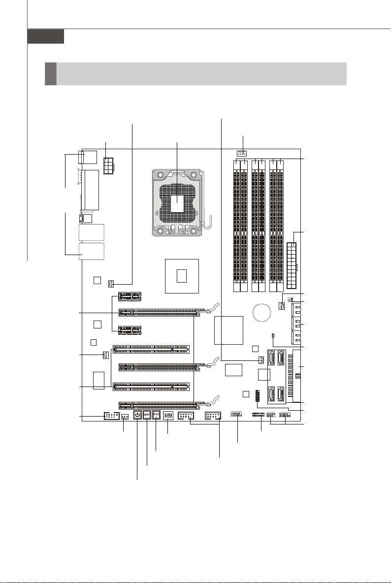
Quick Components Guide
Back Panel,
En-14
PCI_E,
En-23
SYSFAN1,
En-18
PCI,
En-24
J1394_1,
En-18
SYSFAN4, En-18
JPWR2, En-13
SYSFAN5, En-18
CPU, En-5
123
CPU_CLK1,En-25
DLED2, En-22
RESET1, En-22
POWER1, En-22
SYSFAN2, En-18
CPUFAN, En-18
JCOM1, En-19
JUSB1~2, En-21
JTPM1, En-20
DDR3, En-9
JPWR1, En-13
SYSFAN3, En-18
JSMB1, En-21
SATA, En-17
JCI1, En-20
IDE1, En-16
SATA, En-17
JDLED2, En-20
JFP2, JFP1,
En-19
En-4
Page 14
CPU (Central Processing Unit)
When you are installing the CPU, make sure to install the cooler to prevent
overheating. If you do not have the CPU cooler, consult your dealer before turning
on the computer.
For the latest information about CPU, please visit http://global.msi.com.tw/index.
php?func=cpuform2
Important
Overheating
Overheating will seriously damage the CPU and system. Always make sure
the cooling fan can work properly to protect the CPU from overheating. Make
sure that you apply an even layer of thermal paste (or thermal tape) between
the CPU and the heatsink to enhance heat dissipation.
Replacing the CPU
While replacing the CPU, always turn off the ATX power supply or unplug the
power supply’s power cord from the grounded outlet first to ensure the safety
of CPU.
Overclocking
This mainboard is designed to support overclocking. However, please make
sure your components are able to tolerate such abnormal setting, while
doing overclocking. Any attempt to operate beyond product specifications is
not recommended. We do not guarantee the damages or risks caused
by inadequate operation or beyond product specifications.
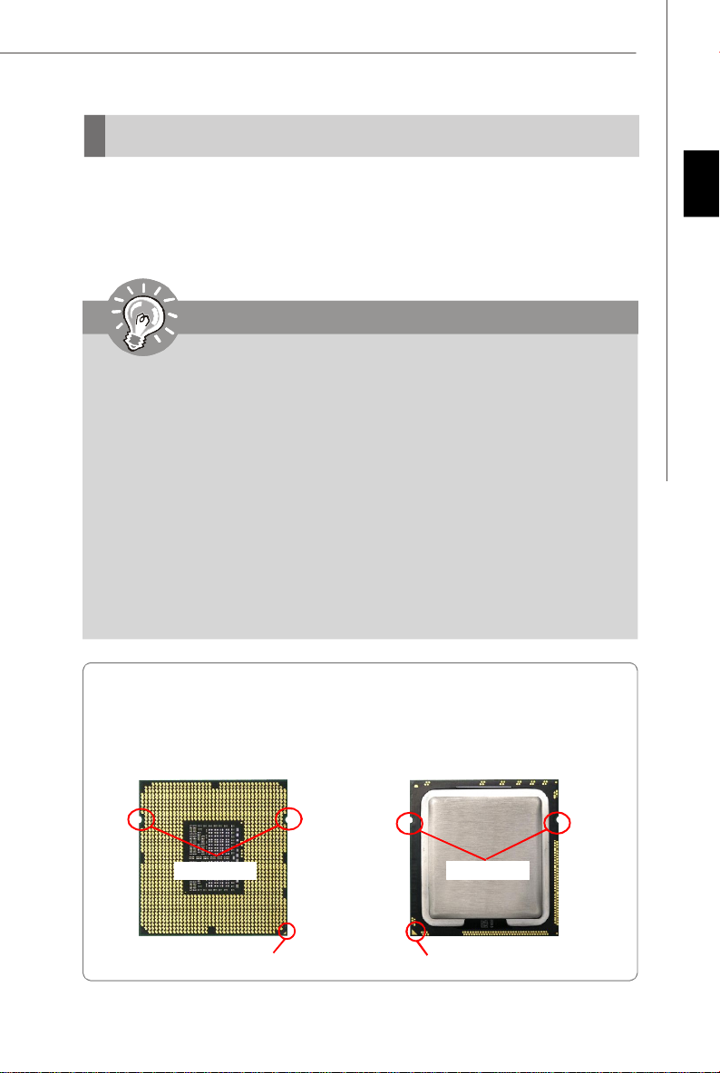
Introduction to LGA 1366 CPU
The pin-pad side of LGA 1366
CPU.
The surface of LGA 1366 CPU.
Remember to apply some thermal paste on it for better heat
dispersion.
English
Alignment Key
Yellow triangle is the Pin 1 indicator
Alignment Key
Yellow triangle is the Pin 1 indicator
En-5
Page 15
MS-7520 Mainboard
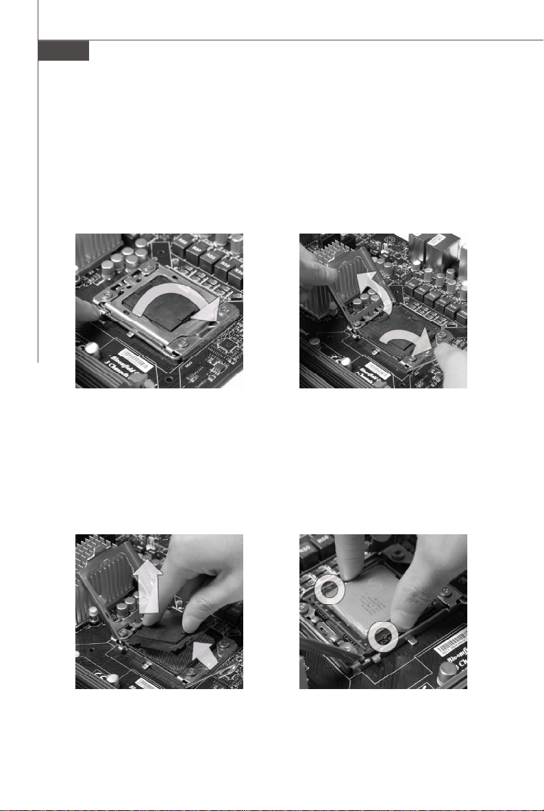
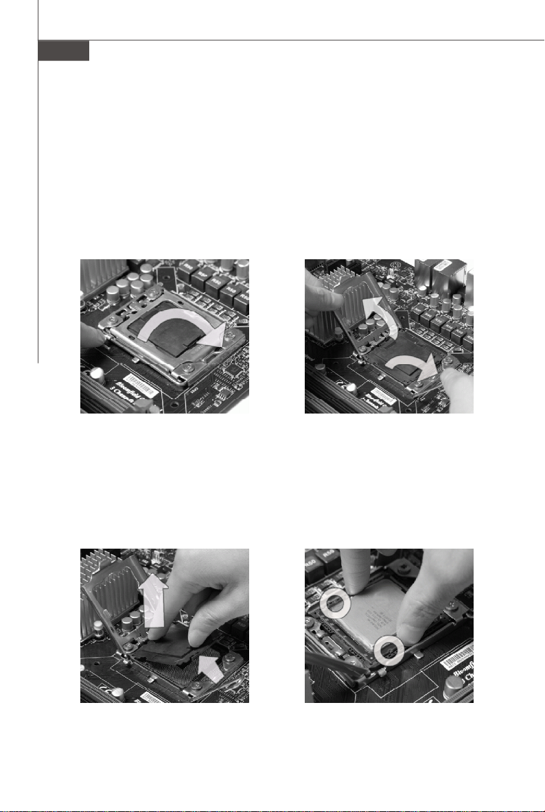
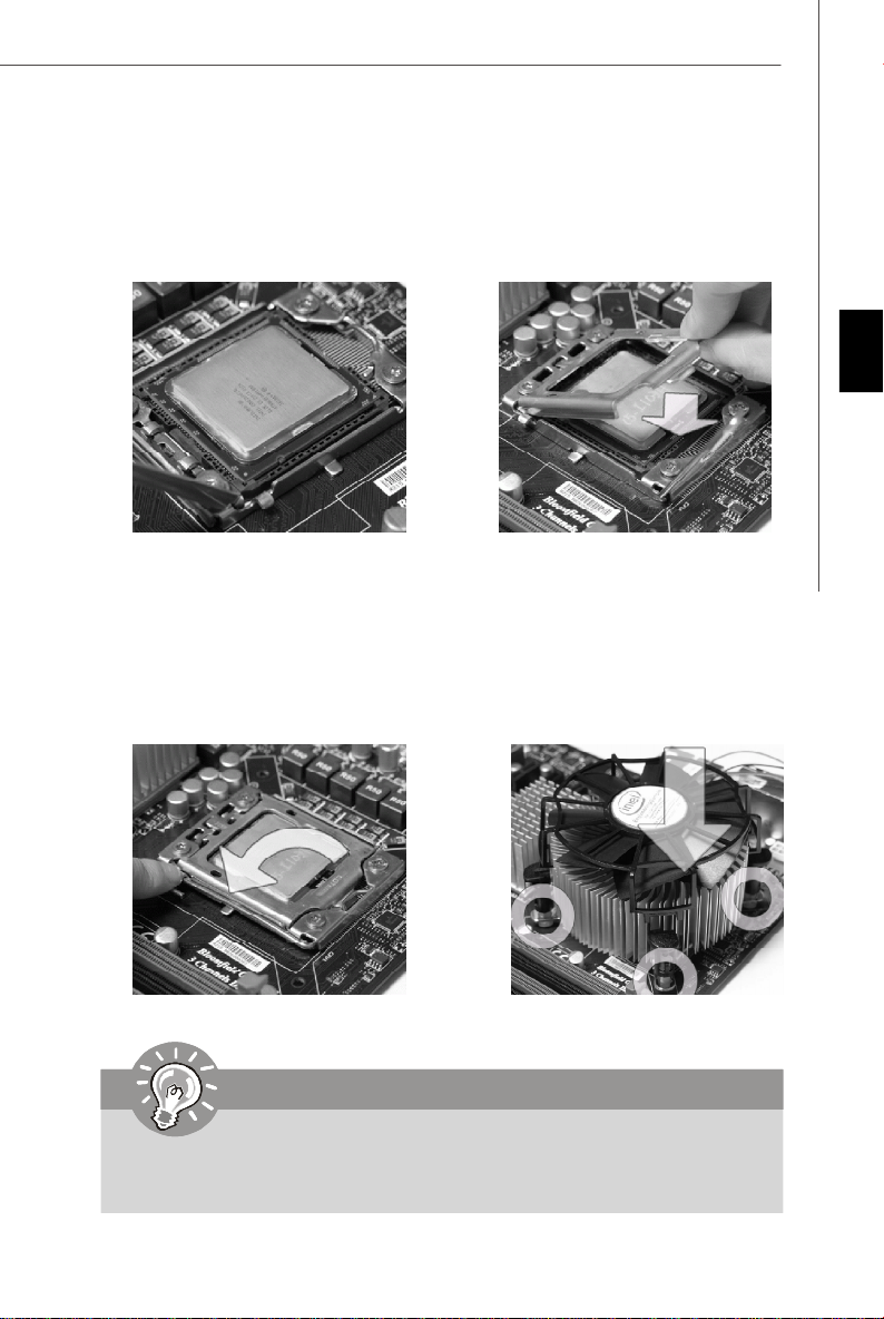
CPU & Cooler Installation
When you are installing the CPU, make sure the CPU has a cooler attached on
the top to prevent overheating. Meanwhile, do not forget to apply some thermal
paste on CPU before installing the heat sink/cooler fan for better heat dispersion.
Follow the steps below to install the CPU & cooler correctly. Wrong installation will
cause the damage of your CPU & mainboard.
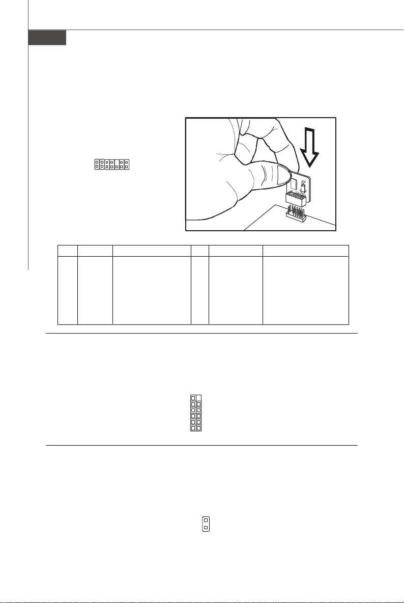
1. Open the load level.
3. The CPU socket has a plastic cap on
it to protect the contack from damage.
Before you install CPU, always cover
it to protect the socket pin. Romove
the cap from the lever hinge side (as
the arrow shows).
2.Lift the load lever up and open the
load plate.
4.After confirming the CPU direction for
correct mating, put down the CPU in
the socket housing frame. Be sure
to grasp on the edge of the CPU base.
Note that the alignment keys are
matched.
En-6
alignment key
Page 16
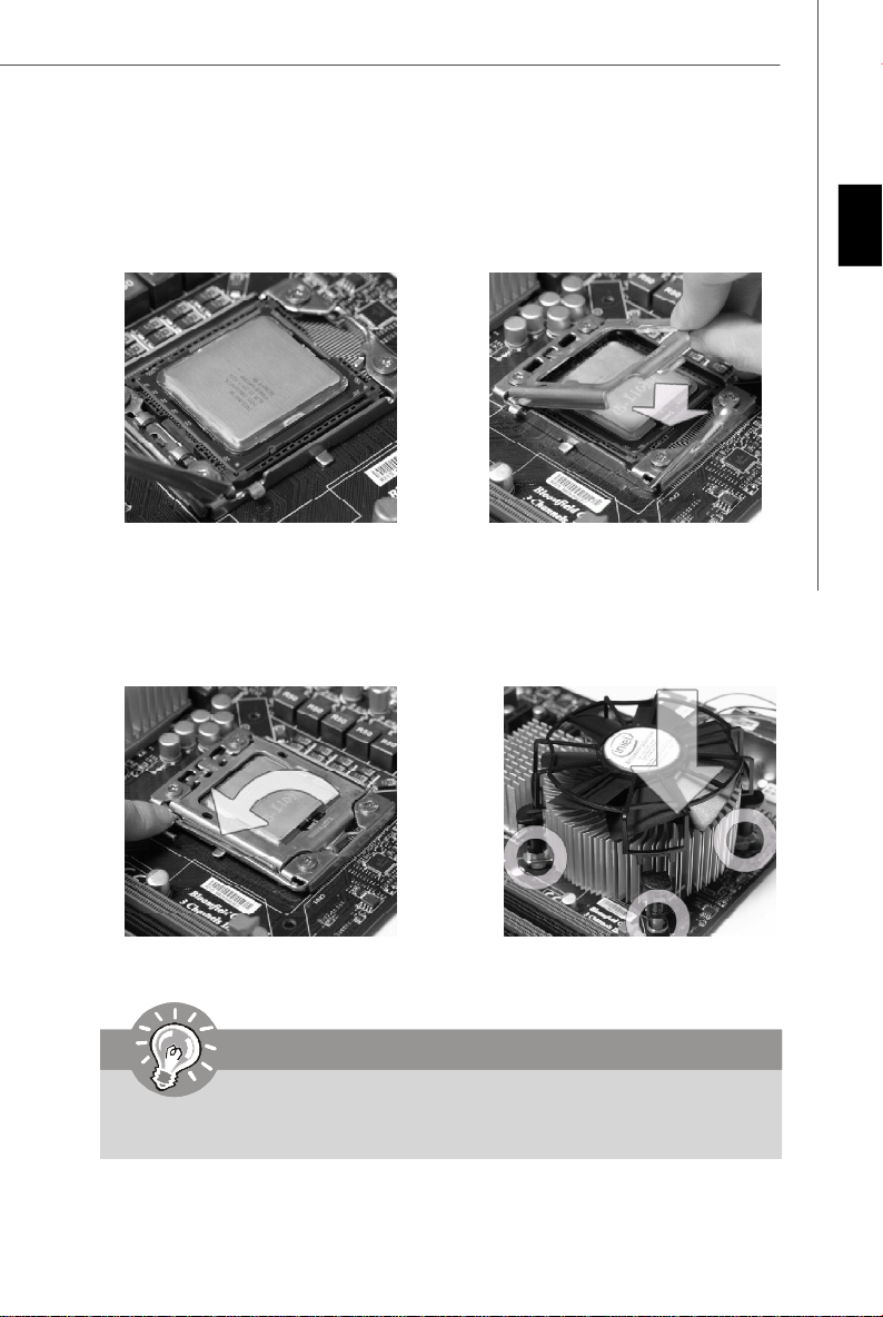
5.Visually inspect if the CPU is seated
well into the socket. If not, take out
the CPU with pure vertical motion and
reinstall.
6.Cover the load plate onto the
package.
English
7.Press down the load lever lightly onto
the load plate, and then secure the
lever with the hook under retention
tab.
8.Align the holes on the mainboard with
the heatsink. Push down the cooler
until its four clips get wedged into
the holes of the mainboard.
Important
1.Confirm if your CPU cooler is firmly installed before turning on your system.
2. Do not touch the CPU socket pins to avoid damaging.
En-7
Page 17
MS-7520 Mainboard
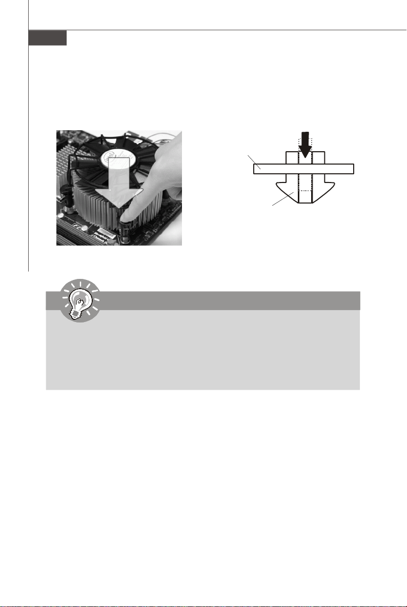
9.Press the four hooks down to fasten
the cooler.
10. Turn over the mainboard to confirm
that the clip-ends are correctly
inserted.
Mainboard
locking switch
Hook
Important
1. Read the CPU status in BIOS.
2. Whenever CPU is not installed, always protect your CPU socket pin with the
plastic cap covered (shown in Figure 1) to avoid damaging.
3. Mainboard photos shown in this section are for demonstration of the CPU/
cooler installation only. The appearance of your mainboard may vary depending on the model you purchase.
En-8
Page 18
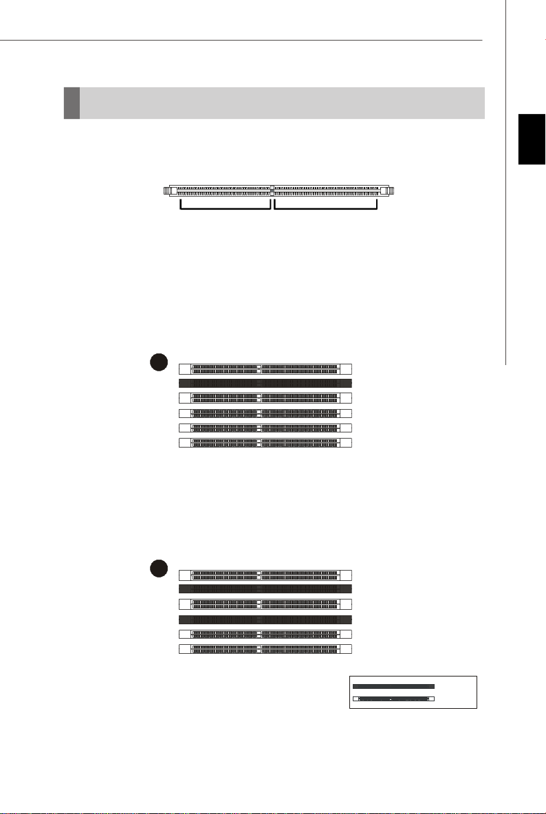
Memory
Installed
1
2
These DIMM slots are used for installing memory modules.
For more information on compatible components, please visit http://global.msi.com.
tw/index.php?func=testreport
DDR3
240-pin, 1.5V
48x2=96 pin
Memory Population Rules
Please refer to the following illustrations for memory population rules.
Single-Channel mode
When you have only one memory module, please always insert it into the DIMM_A0
first (as way 1 shown in below).
Dual-Channel mode
In Dual-Channel mode, the memory modules can transmit and receive data with two
data bus lines simultaneously. Enabling Dual-Channel mode can enhance the system
performance. When you have two memory modules, please always insert them into
the DIMM_A0 & DIMM_B0 (as way 2 shown in below).
72x2=144 pin
DIMM_A1
DIMM_A0
DIMM_B1
DIMM_B0
DIMM_C1
DIMM_C0
English
DIMM_A1
DIMM_A0
DIMM_B1
DIMM_B0
DIMM_C1
DIMM_C0
Empty
En-9
Page 19

MS-7520 Mainboard
3
4
5
6
Three-Channel mode
In Three-Channel mode, the memory modules can transmit and receive data with
three data bus lines simultaneously. Enabling Three-Channel mode can enhance the
best system performance. When you have three or more memory modules, please
always insert them as the way 3/ 4/ 5/ 6 (shown in below) to get the best system
performance.
DIMM_A1
DIMM_A0
DIMM_B1
DIMM_B0
DIMM_C1
DIMM_C0
DIMM_A1
DIMM_A0
DIMM_B1
DIMM_B0
DIMM_C1
DIMM_C0
DIMM_A1
DIMM_A0
DIMM_B1
DIMM_B0
DIMM_C1
DIMM_C0
DIMM_A1
DIMM_A0
DIMM_B1
DIMM_B0
DIMM_C1
DIMM_C0
En-10
Page 20
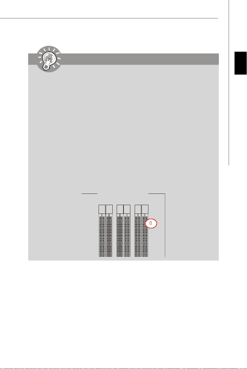
Important
DIMM_A1DIMM_A0DIMM_B1DIMM_C1DIMM_B0DIMM_C
0
-DDR3 memory modules are not interchangeable with DDR2 and the DDR3
standard is not backwards compatible. You should always install DDR3
memory modules in the DDR3 DIMM slots.
-In Three-/ Dual- channel mode, make sure that you install memory modules
of the same type and density in different channel DIMM slots. If the speeds
of installed memeory modules are different (ex. 1066 & 1333), the system will
detect and operate the lower speed (1066) with all installed memory modules.
- Please always install the same type and density memory modules in DIMM
slots to avoid the damage of memory.
-To enable successful system boot-up, always insert the memory modules
into the DIMM_A0 first.
- Due to the chipset resource deployment, the system density will only be
detected up to 23+GB (not full 24GB) when each DIMM is installed with a 4GB
memory module.
- When you install incorrect memory module (the SA2-pin of the memory
module connects to Ground) in the DIMM_C0/C1, the LED beside DIMM_C0
will light red color to remind you. The position of the LED is shown as below.
Double confirm with your memory module vender for the third channelsupports.
English
En-11
Page 21

MS-7520 Mainboard
Installing Memory Modules
1. The memory module has only one notch on the center and will only fit in the right
orientation.
2. Insert the memory module vertically into the DIMM slot. Then push it in until the
golden finger on the memory module is deeply inserted in the DIMM slot. The plastic
clip at each side of the DIMM slot will automatically close when the memory module
is properly seated.
Important
You can barely see the golden finger if the memory module is properly inserted
in the DIMM slot.
3. Manually check if the memory module has been locked in place by the DIMM slot
clips at the sides.
En-12
Volt
Notch
Page 22
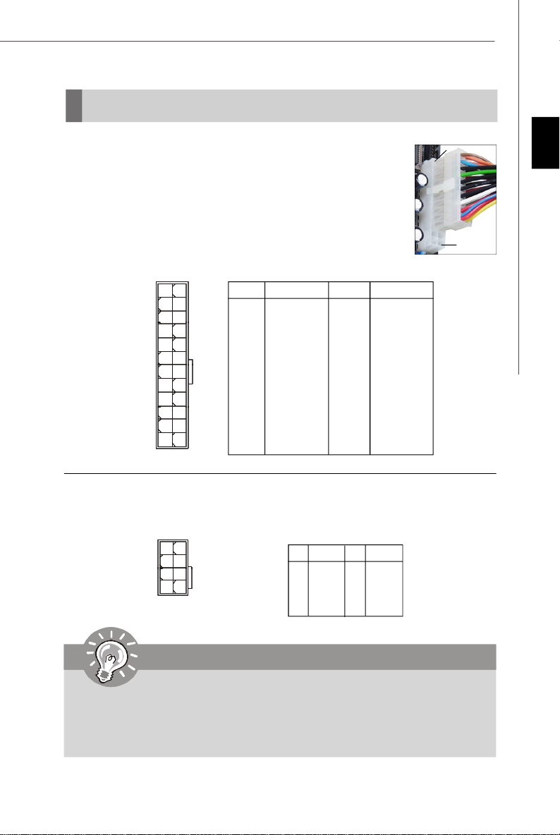
Power Supply
ATX 24-Pin Power Connector: JPWR1
This connector allows you to connect an ATX 24-pin power supply.
To connect the ATX 24-pin power supply, make sure the plug of the
power supply is inserted in the proper orientation and the pins are
aligned. Then push down the power supply firmly into the connector.
You may use the 20-pin ATX power supply as you like. If you’d like
to use the 20-pin ATX power supply, please plug your power supply along with pin 1 & pin 13 (refer to the image at the right hand).
Pin Definition
PIN SIGNAL
13 +3.3V
14 -12V
15 GND
16 PS-ON#
17 GND
18 GND
19 GND
20 Res
21 +5V
22 +5V
23 +5V
24 GND
JPWR1
12
1
24
13
PIN SIGNAL
1 +3.3V
2 +3.3V
3 GND
4 +5V
5 GND
6 +5V
7 GND
8 PWR OK
9 5VSB
10 +12V
11 +12V
12 +3.3V
ATX 12V Power Connector: JPWR2
This power connector is used to provide power to the CPU.
Pin Definition
PINSIGNAL
1 GND
2 GND
3 GND
4 GND
PINSIGNAL
5 +12V
6 +12V
7 +12V
8 +12V
JPWR2
4
1
8
5
pin 13
pin 12
English
Important
1. Make sure that all the connectors are connected to proper ATX power supplies to ensure stable operation of the mainboard.
2. Power supply of 450 watts (and above) is highly recommended for system
stability.
3. ATX 12V power connection should be greater than 18A.
En-13
Page 23
MS-7520 Mainboard
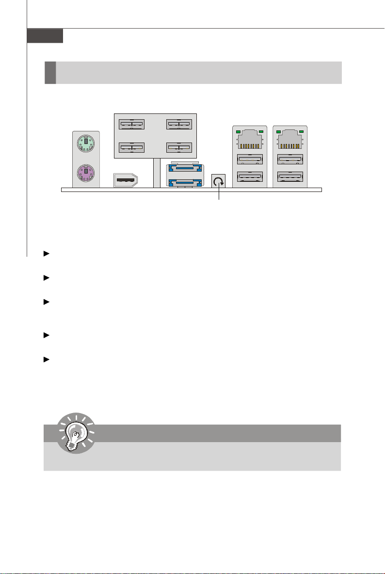
Back Panel
Mouse
Keyboard
USB Ports
LAN
LAN
1394 Port
eSATA Ports
Clear CMOS
Button
USB Ports
USB Ports
Mouse/Keyboard
The standard PS/2® mouse/keyboard DIN connector is for a PS/2® mouse/keyboard.
1394 Port
The IEEE1394 port on the back panel provides connection to IEEE1394 devices.
USB Port
The USB (Universal Serial Bus) port is for attaching USB devices such as keyboard,
mouse, or other USB-compatible devices.
eSATA Port
The eSATA port is for attaching the eSATA external hard drive.
Clear CMOS Button
There is a CMOS RAM on board that has a power supply from external battery to
keep the system configuration data. With the CMOS RAM, the system can automatically boot OS every time it is turned on. If you want to clear the system configuration,
use the button to clear data. Press the button to clear the data.
Important
Make sure that you power off the system before clearing CMOS data.
En-14
Page 24
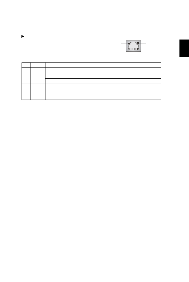
LAN
The standard RJ-45 LAN jack is for connection to
the Local Area Network (LAN). You can connect a
network cable to it.
LED Color LED State Condition
Off LAN link is not established.
Left Yellow On (steady state) LAN link is established.
On (brighter & pulsing)The computer is communicating with another computer on the LAN.
Green Off 10 Mbit/sec data rate is selected.
Right On 100 Mbit/sec data rate is selected.
Orange On 1000 Mbit/sec data rate is selected.
Green / OrangeYellow
English
En-15
Page 25
MS-7520 Mainboard
Connectors
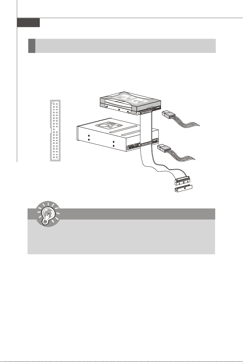
IDE Connector: IDE1
This connector supports IDE hard disk drives, optical disk drives and other IDE devices.
Important
If you install two IDE devices on the same cable, you must configure the
drives separately to master / slave mode by setting jumpers. Refer to IDE
device’s documentation supplied by the vendors for jumper setting
instructions.
En-16
Page 26
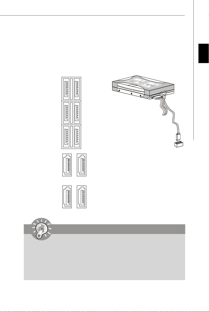
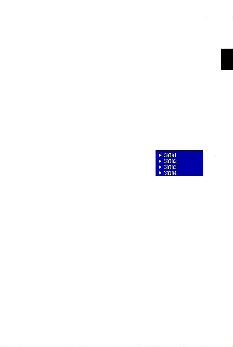
Serial ATA Connector: SATA1~10
This connector is a high-speed Serial ATA interface port. Each connector can
connect to one Serial ATA device.
SATA1~6 stack SATA connectors
are supported by ICH10R
SATA1_3
SATA2_4
SATA5_6
English
SATA7
SATA9
SATA8
SATA10
SATA7 & 8 are controlled
by 1st JMB322
SATA9 & 10 are controlled
by 2nd JMB322
Important
1. Please do not fold the Serial ATA cable into 90-degree angle. Otherwise,
data loss may occur during transmission.
2. Please always use the Intel default Black SATA connectors (SATA1~6)
first.
3. SATA7 & SATA8, SATA9 & SATA10, support RAID 0/ RAID 1/ JBOD function
and you can set RAID mode in BIOS setup or in DRIVE BOOSTER
MANAGER.
En-17
Page 27
MS-7520 Mainboard
Fan Power Connectors: CPUFAN, SYSFAN1~5
The fan power connectors support system cooling fan with +12V. When connecting
the wire to the connectors, always note that the red wire is the positive and should
be connected to the +12V; the black wire is Ground and should be connected to GND.
If the mainboard has a System Hardware Monitor chipset on-board, you must use a
specially designed fan with speed sensor to take advantage of the CPU fan control.
SE NS OR
GND
+1 2V
CONTROL
CPUFAN
GND
+12V
SENSOR
SYSFAN1
SENSOR
+12V
GND
SYSFAN2/3
GND
+12V
NC
SYSFAN4
+12V
NC
GND
SYSFAN5
Important
1.Please refer to the recommended CPU fans at processor’s official website
or consult the vendors for proper CPU cooling fan.
2.CPUFAN supports fan control. You can install Overclocking Center utility that will automatically control the CPU fan speed according to the actual
CPU temperature.
3. SYSFAN1~3 support fan control, too. You may select how the percentage of
speed for the SYSFAN1/2/3 in BIOS.
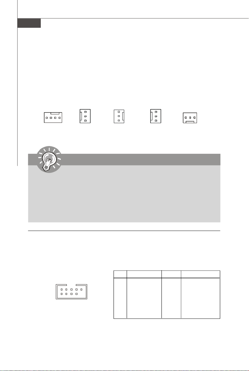
IEEE1394 Connector: J1394_1
This connector allows you to connect the IEEE1394 device via an optional IEEE1394
bracket.
Pin Definition
PIN SIGNAL PIN SIGNAL
1 TPA+ 2 TPA3 Ground 4 Ground
5 TPB+ 6 TPB7 Cable power 8 Cable power
9 Key (no pin) 10 Ground
En-18
J1394_1
2 10
1
9
Page 28
Front Panel Connectors: JFP1, JFP2
These connectors are for electrical connection to the front panel switches and LEDs.
The JFP1 is compliant with Intel® Front Panel I/O Connectivity Design Guide.
JFP1 Pin Definition
PIN SIGNAL DESCRIPTION
1 HD_LED + Hard disk LED pull-up
2 FP PWR/SLP MSG LED pull-up
3 HD_LED - Hard disk active LED
10
9
4 FP PWR/SLP MSG LED pull-up
5 RST_SW - Reset Switch low reference pull-down to GND
6 PWR_SW + Power Switch high reference pull-up
7 RST_SW + Reset Switch high reference pull-up
8 PWR_SW - Power Switch low reference pull-down to GND
9 RSVD_DNU Reserved. Do not use.
JFP2 Pin Definition
PIN SIGNAL DESCRIPTION
1 GND Ground
2 SPK- Speaker-
8
7
3 SLED Suspend LED
4 BUZ+ Buzzer+
5 PLED Power LED
6 BUZ- Buzzer7 NC No connection
8 SPK+ Speaker+
JFP1
JFP2
Power
LED
2
1
2
1
+
- -
HDD
LED
Speaker
+
Power
LED
Power
Switch
-
+
+
Reset
Switch
+
-
English
Serial Port Connector: JCOM1
This connector is a 16550A high speed communication port that sends/receives 16
bytes FIFOs. You can attach a serial device.
Pin Definition
JCOM1
2
1 9
10
PIN SIGNAL DESCRIPTION
1 DCD Data Carry Detect
2 SIN Serial In or Receive Data
3 SOUT Serial Out or Transmit Data
4 DTR Data Terminal Ready
5 GND Ground
6 DSR Data Set Ready
7 RTS Request To Send
8 CTS Clear To Send
9 RI Ring Indicate
En-19
Page 29
MS-7520 Mainboard
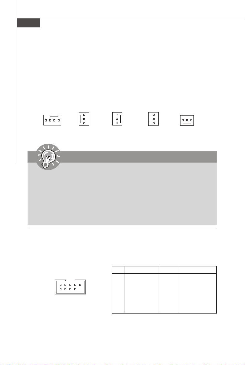
TPM Module Connector: JTPM1
This connector connects to a TPM (Trusted Platform Module) module (optional). Please
refer to the TPM security platform manual for more details and usages.
2
1
Pin Signal Description Pin Signal Description
1 LCLK LPC clock 2 3V_STB 3V standby power
3 LRST# LPC reset 4 VCC3 3.3V power
5 LAD0 LPC address & data pin0 6 SIRQ Serial IRQ
7 LAD1 LPC address & data pin1 8 VCC5 5V power
9 LAD2 LPC address & data pin2 10 KEY No pin
11 LAD3 LPC address & data pin3 12 GND Ground
13 LFRAME# LPC Frame 14 GND Ground
14
13
D-LED2 Panel Connector: JDLED2
This connector connects to a D-LED2 (Debug-LED2) panel (optional), which shows
information on the panel for you and identify the current status or mode of the
connected system. Please refer to the D-LED2 quick guide for more details and
usages.
1112
12
Chassis Intrusion Connector: JCI1
This connector connects to the chassis intrusion switch cable. If the chassis is
opened, the chassis intrusion mechanism will be activated. The system will record
this status and show a warning message on the screen. To clear the warning, you
must enter the BIOS utility and clear the record.
GND
2
CINTRU
En-20
1
JCI1
Page 30
Front USB Connector: JUSB1/ JUSB2
These connectors, compliant with Intel® I/O Connectivity Design Guide, is ideal for
connecting high-speed USB interface peripherals such as USB HDD, digital cameras,
MP3 players, printers, modems and the like.
Pin Definition
JUSB1/ JUSB2
2
1
10
9
PIN SIGNAL PIN SIGNAL
1 VCC 2 VCC
3 USB0- 4 USB15 USB0+ 6 USB1+
7 GND 8 GND
9 Key (no pin) 10 NC
USB 2.0 Bracket
Important
English
Note that the pins of VCC and GND must be connected correctly to avoid
possible damage.
GreenPower Genie Connector: JSMB1
This connector connects to GreenPower Genie (optional). Please refer to the
GreenPower Genie manual for more details and usages.
1
2
JSMB1
En-21
Page 31

MS-7520 Mainboard
Buttons
The motherboard provides the following buttons for you to set the computer’s function.
This section will explain how to change your motherboard’s function through the use
of button.
Power Button: POWER1
This power button is used to turn-on or turn-off the system. Press the button to turnon or turn-off the system. This button will light after you power-on the system, and
the light will turn-off when you power-off the system.
POWER1
Reset Button: RESET1
This reset button is used to reset the system. Press the button to reset the system.
This button will light when the system is in S0 status.
RESET1
D-LED2 Change Menu Button: DLED2
This button is used to change the menu on D-LED2 panel. Press the button to change
the menu on D-LED2 panel. Please refer to the D-LED2 quick guide for more details
and usages.
DLED2
En-22
Page 32

Slots
PCI (Peripheral Component Interconnect) Express Slot
The PCI Express slot supports the PCI Express interface expansion card.
The PCI Express 2.0 x16 supports up to 8.0 GB/s transfer rate.
The PCI Express 2.0 x4 supports up to 2.0 GB/s transfer rate.
The PCI Express x1 supports up to 250 MB/s transfer rate.
Black PCI Express x16 Slots support up to
PCI Express 2.0 x16 speed (PCI_E2 & PCI_E4)
PCI Express x1 Slots supports up to
PCI Express x1 speed (PCI_E1 & PCI_E3)
Blue PCI Express x16 Slot supports up to
PCI Express 2.0 x4 speed (PCI_E5)
English
Important
The mainboard supports ATI CrossFireXTM technology with two Black PCIE
x16 slots and 3-way CrossFireXTM with all the three PCIE x16 slots.
En-23
Page 33

MS-7520 Mainboard
PCI (Peripheral Component Interconnect) Slot
The PCI slot supports LAN card, SCSI card, USB card, and other add-on cards that
comply with PCI specifications.
32-bit PCI Slot
Important
When adding or removing expansion cards, make sure that you unplug the
power supply first. Meanwhile, read the documentation for the expansion card
to configure any necessary hardware or software settings for the expansion
card, such as jumpers, switches or BIOS configuration.
PCI Interrupt Request Routing
The IRQ, acronym of interrupt request line and pronounced I-R-Q, are hardware lines
over which devices can send interrupt signals to the microprocessor. The PCI IRQ
pins are typically connected to the PCI bus pins as follows:
Order 1 Order 2 Order 3 Order 4
PCI Slot 1 INT A# INT B# INT C# INT D#
PCI Slot 2 INT B# INT C# INT D# INT A#
En-24
Page 34

Switch
Hardware Overclock Base clock Switch: CPU_CLK1
You can overclock the Base clock to increase the processor frequency by changing
this switch. Follow the instructions below to set the base clock.
ON
123
133 MHz (default)
ON
123
166 MHz 200 MHz
ON
123
Important
1. Make sure that you power off the system before changing the switch.
2. This overclocking behavior depends on the system’s configuration (memory
capability, thermal solution...etc), and it is not guaranteed.
3. HW overclocking may cause instability or crash during boot, then please
re-set the switch to default.
4. You can also overclock by setting BIOS. BIOS overclocking may also
cause crash during boot and then please reboot the system 3 times to
restore default BIOS settings. For more details, please refer to the BIOS
chapter.
English
En-25
Page 35

MS-7520 Mainboard
DDR Phase LEDs
DIMM warning LED
ON
LED Status Indicators
CPU Phase LEDs
QPI Phase LEDs
IOH Phase LEDs
PCIE LED
PCIE LED
PCIE LED
PCI LED
PCIE LED
PCI LED
Power LED
PCIE LED
Standby LED
123
En-26
Page 36
Name Status
CPU Phase LEDs 6 (5/ 4/ 3/ 2/ 1) LED(s) will light blue when CPU is in
6 (5/ 4/ 3/ 2/ 1) phase power mode.
QPI Phase LEDs 1 LED (2 LEDs) will light blue when QPI is in 1 (2)
phase power mode.
IOH Phase LEDs 1 LED (2 LEDs) will light blue when IOH (north bridge) is
in 1 (2) phase power mode.
DDR Phase LEDs 1 LED (2 LEDs) of the LEDs will light blue when the
memory is in 1 (2) phase power mode.
PCI E LEDs Lights blue when the PCIE Slot is functional.
PCI LEDs Lights blue when the PCI Slot is functional.
Power LED Lights green when the system is in power-on (S0/S1)
status.
Standby LED Lights orange when the system is in standby (S3/S4/S5 )
status.
DIMM Warning LED Lights red when the incorrect memory installed into
DIMM_C0/ DIMM_C1 (the DIMMs of 3rd channel).
Important
You can install the Green Power Center utility, that allows you to disable these
LEDs separetely or all together. Or you may disable all the LEDs in BIOS
setup (Green Power menu).
English
En-27
Page 37

MS-7520 Mainboard
BIOS Setup
This chapter provides basic information on the BIOS Setup program and allows you
to configure the system for optimum use. You may need to run the Setup program
when:
* An error message appears on the screen during the system booting up, and requests
you to run BIOS SETUP.
* You want to change the default settings for customized features.
Important
1.The items under each BIOS category described in this chapter are under
continuous update for better system performance. Therefore, the description
may be slightly different from the latest BIOS and should be held for reference
only.
2.Upon boot-up, the 1st line appearing after the memory count is the BIOS
version. It is usually in the format:
1st digit refers to BIOS maker as A = AMI, W = AWARD, and P = PHOENIX.
2nd - 5th digit refers to the model number.
6th refers to the Chipset vender as A = AMD, I = Intel, V = VIA, N = Nvidia, U =
ULi.
7th - 8th digit refers to the customer as MS = all standard customers.
V1.0 refers to the BIOS version.
101808 refers to the date this BIOS was released.
A7520IMS V1.0 101808 where:
En-28
Page 38
Entering Setup
Power on the computer and the system will start POST (Power On Self Test) process.
When the message below appears on the screen, press <DEL> key to enter Setup.
Press DEL to enter SETUP
If the message disappears before you respond and you still wish to enter Setup,
restart the system by turning it OFF and On or pressing the RESET button. You may
also restart the system by simultaneously pressing <Ctrl>, <Alt>, and <Delete> keys.
Getting Help
After entering the Setup menu, the first menu you will see is the Main Menu.
Main Menu
The main menu lists the setup functions you can make changes to. You can use the
arrow keys (↑↓ ) to select the item. The on-line description of the highlighted setup
function is displayed at the bottom of the screen.
Sub-Menu
If you find a right pointer symbol (as shown in the right view)
appears to the left of certain fields that means a sub-menu
containing additional options can be launched from this field.
You can use control keys (↑↓ ) to highlight the field and
press <Enter> to call up the sub-menu. Then you can use the
control keys to enter values and move from field to field within a sub-menu. If you
want to return to the main menu, just press <Esc >.
General Help <F1>
The BIOS setup program provides a General Help screen. You can call up this screen
from any menu by simply pressing <F1>. The Help screen lists the appropriate keys
to use and the possible selections for the highlighted item. Press <Esc> to exit the
Help screen.
English
En-29
Page 39

MS-7520 Mainboard
The Main Menu
Once you enter AMI® or AWARD® BIOS CMOS Setup Utility, the Main Menu will appear
on the screen. The Main Menu allows you to select from the setup functions and two
exit choices. Use arrow keys to select among the items and press <Enter> to accept
or enter the sub-menu.
Standard CMOS Features
Use this menu for basic system configurations, such as time, date etc.
Advanced BIOS Features
Use this menu to setup the items of special enhanced features.
Integrated Peripherals
Use this menu to specify your settings for integrated peripherals.
Power Management Setup
Use this menu to specify your settings for power management.
H/W Monitor
This entry shows your PC health status. .
Green Power
Use this menu to specify the power phase.
BIOS Setting Password
Use this menu to set the Password.
Cell Menu
Use this menu to specify your settings for frequency/voltage control and overclocking.
User Settings
Use this menu to save/ load your settings to/ from CMOS for BIOS.
M-Flash
Use this menu to read/ flash the BIOS from storage drive (FAT/ FAT32 format only).
Load Fail-Safe Defaults
Use this menu to load the default values set by the BIOS vendor for stable system
performance.
Load Optimized Defaults
Use this menu to load the default values set by the mainboard manufacturer specifically
for optimal performance of the mainboard.
Save & Exit Setup
Save changes to CMOS and exit setup.
Exit Without Saving
Abandon all changes and exit setup.
En-30
Page 40
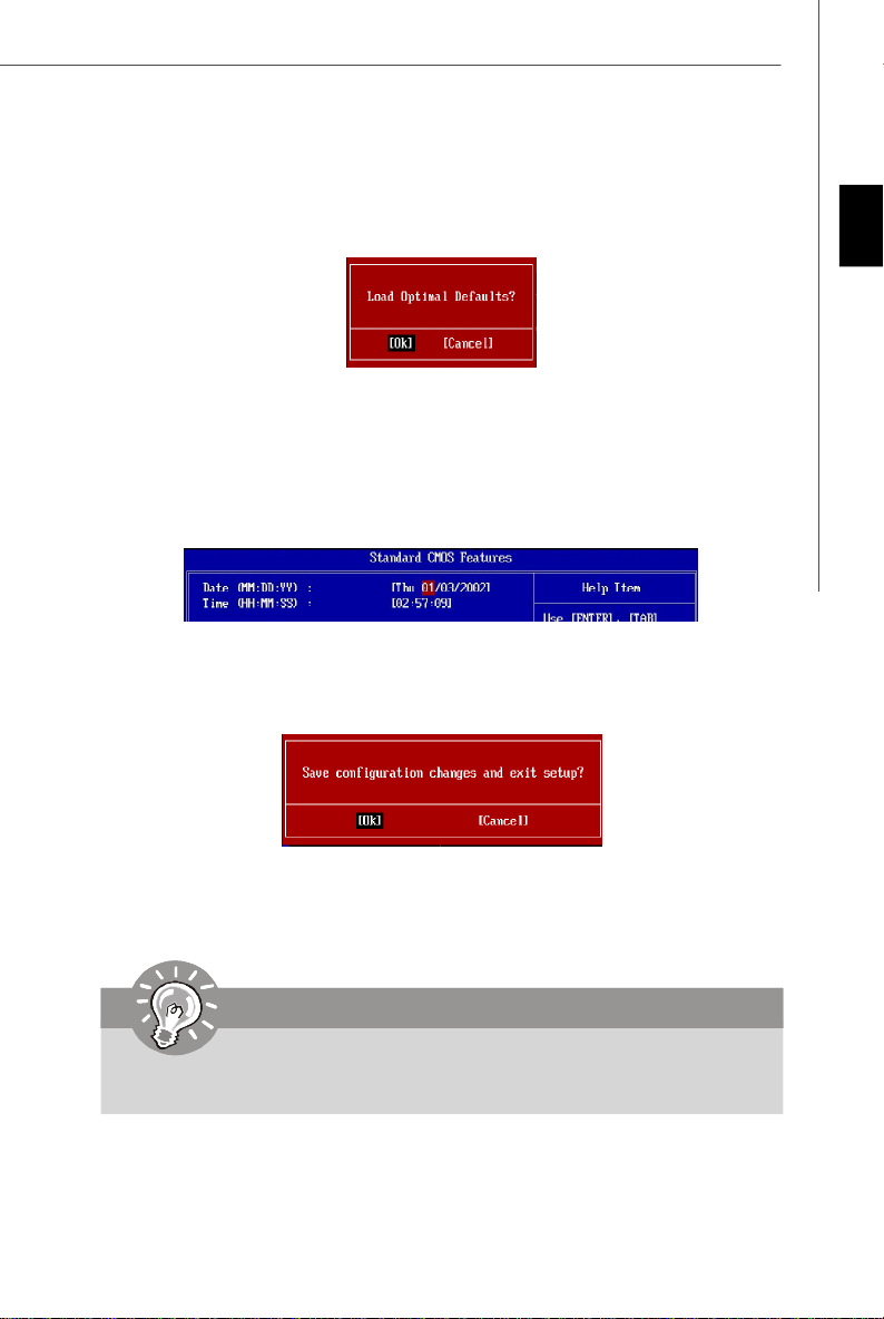
When enter the BIOS Setup utility, follow the processes below for general use.
1. Load Optimized Defaults : Use control keys (↑↓) to highlight the Load
Optimized Defaults field and press <Enter> , a message as below appears:
Select [Ok] and press Enter to load the default settings for optimal system
performance.
2. Setup Date/ Time : Select the Standard CMOS Features and press <Enter> to
enter the Standard CMOS Features-menu. Adjust the Date, Time fields.
3. Save & Exit Setup : Use control keys (↑↓) to highlight the Save & Exit Setup
field and press <Enter> , a message as below appears:
English
Select [Ok] and press Enter to save the configurations and exit BIOS Setup utility.
Important
The configuration above are for general use only. If you need the detailed
settings of BIOS, please read the manual in English version on MSI website.
En-31
Page 41

MS-7520 Mainboard
4. Cell Menu Introduction : This menu is for advanced user who want to overclock
the mainboard.
Important
Change these settings only if you are familiar with the chipset.
Current Core / DRAM / QPI Frequency
These items show the current clocks of CPU and Memory speed. Read-only.
En-32
Page 42

CPU Specifications
Press <Enter> to enter the sub-menu. The sub-menu displays the informations
of installed CPU.
CPU Technology Support
Press <Enter> to enter the sub-menu. The sub-menu displays the technologies
that the installed CPU supported.
D.O.T. Control
D.O.T. (Dynamic Overclocking Technology) is an automatic overclocking function,
included in the MSITM’s newly developed Overclocking Center Technology. It is designed
to detect the load balance of CPU while running programs, and to adjust the best
frequency automatically. When the motherboard detects system is running programs,
it will speed up automatically to make the program run smoothly and faster. When the
system is temporarily suspending or staying in the low load balance, it will restore the
default settings instead. Usually the Dynamic Overclocking Technology will be powered only when users' PC need to run huge amount of data like 3D games or the video
process, and the CPU frequency need to be boosted up to enhance the overall
performance.
Important
Even though the Dynamic Overclocking Technology is more stable than
manual overclocking, basically, it is still risky. We suggest user to make
sure that your CPU can afford to overclocking regularly first. If you find the
PC appears to be unstable or reboot incidentally, it's better to disable the
Dynamic Overclocking or to lower the level of overclocking options. By the
way, if you need to conduct overclocking manually, you also need to disable
the Dynamic OverClocking first.
English
Intel EIST
The Enhanced Intel SpeedStep technology allows you to set the performance level of
the microprocessor whether the computer is running on battery or AC power. This
field will appear after you installed the CPU which support speedstep technology.
Intel C-STATE tech
C-state is a power management state that significantly reduces the power of the
processor during idle. This field will appear after you installed the CPU which support
c-state technology.
Base Clock (MHz)
This item allows you to set the CPU Base clock (in MHz). You may overclock the CPU
by adjusting this value. Please note the overclocking behavior is not guaranteed.
En-33
Page 43

MS-7520 Mainboard
Intel Turbo Boost tech
This item will appear when you install a CPU with Intel Turbo Boost technology. This
item is used to enable/ disable Intel Turbo Boost technology. It can scale processor
frequency higher dynamically when applications demand more performance and TDP
headroom exists. It also can deliver seamless power scalability (Dynamically scale
up, Speed-Step Down). It is the Intel newly technology within i7 CPU.
Turbo Boost Tech Config
This sub-menu will appear when you install a CPU include Intel Turbo Boost technology.
Press <Enter> to enter the sub-menu.
Turbo Ratio Limit Program
This item is used to enable/ disable the turbo ratio limit program. Setting to [Enable]
activates the following fields, and use the following fields to set each CPU core
ratio.
1/2/3/4-Core Ratio Limit
These items allow you to select the CPU core ratio.
TDC Limit Override
Setting to [Enable] activates the TDC Limit value field, and use the TDC Limit
value field to set the CPU TDC value.
TDC Limit value (A)
This item allows you to select the CPU TDC value (ampere).
TDP Limit Override
Setting to [Enable] activates the TDP Limit value field, and use the TDP Limit
value field to set the CPU TDP value.
TDP Limit value (W)
This item allows you to select the CPU TDP value (watt).
Adjusted Core Frequency (MHz)
It shows the adjusted CPU frequency (Base clock x Ratio). Read-only.
QPI Configuration
Press <Enter> to enter the sub-menu.
QPI Links Speed
This item allows you to select the QPI links speed type.
QPI Frequency
This item allows you to select the QPI frequency.
Memory-Z
Press <Enter> to enter the sub-menu.
En-34
Page 44

DIMM1~6 Memory SPD Information
Press <Enter> to enter the sub-menu. The sub-menu displays the informations of
installed memory.
Advance DRAM Configuration
Press <Enter> to enter the sub-menu.
1N/2N Memory Timing
This item controls the SDRAM command rate. Select [1N] makes SDRAM signal
controller to run at 1N (N=clock cycles) rate. Selecting [2N] makes SDRAM signal
controller run at 2N rate.
CAS# Latency (CL)
This controls the CAS latency, which determines the timing delay (in clock cycles)
before SDRAM starts a read command after receiving it.
tRCD
When DRAM is refreshed, both rows and columns are addressed separately.
This setup item allows you to determine the timing of the transition from RAS
(row address strobe) to CAS (column address strobe). The less the clock
cycles, the faster the DRAM performance.
tRP
This setting controls the number of cycles for Row Address Strobe (RAS) to be
allowed to precharge. If insufficient time is allowed for the RAS to accumulate its
charge before DRAM refresh, refresh may be incomplete and DRAM may fail to
retain data. This item applies only when synchronous DRAM is installed in the
system.
tRAS
This setting determines the time RAS takes to read from and write to memory
cell.
English
Advanced Memory Setting
Setting to [Auto] enables the advance memory timing automatically to be determined
by BIOS. Setting to [Manual] allows you to set advanced memory timings.
Extreme Memory Profile
This item is used to enable/disable the Intel Extreme Memory Profile (XMP). For further
information please refer to Intel's official website.
Memory Ratio
This item allows you to set the memory multiplier.
Adjusted DRAM Frequency (MHz)
It shows the adjusted DDR Memory frequency. Read-only.
En-35
Page 45

MS-7520 Mainboard
ClockGen Tuner
Press <Enter> to enter the sub-menu.
CPU / PCI Express Amplitude Control
These items are used to select the CPU/ PCI Express clock amplitude.
CPU CLK Skew/ IOH CLK Skew
These items are used to select the CPU/ IOH chipset clock skew. They can help
CPU to reach the higher overclocking performace.
Adjust PCI Frequency (MHz)
This field allows you to select the PCI frequency (in MHz).
Adjust PCI-E Frequency (MHz)
This field allows you to select the PCIE frequency (in MHz).
Auto Disable DRAM/PCI Frequency
When set to [Enabled], the system will remove (turn off) clocks from empty DIMM
and PCI slots to minimize the electromagnetic interference (EMI).
CPU Voltage (V)/ QPI Voltate (V))/ CPU PLL Voltage (V)/ DRAM Voltage (V)/
DDR_VREF_CA_A (V)/ DDR_VREF_CA_B (V)/ DDR_VREF_CA_C (V)/
DDR_VREF_DQ_A (V)/DDR_VREF_DQ_B (V), DDR_VREF_DQ_C (V)/ IOH Voltage
(V), ICH Voltage (V)
These items are used to asjust the voltage of CPU, Memory, QPI and chipset.
For CPU Voltage:
The value here is the offset for you to adjust/add based on the current CPU voltage.
Please read the real-time CPU voltage in “CPU Vcore” in the “H/W monitor” page.
Please note the based CPU Voltage will vary depending on the different CPU you
install.
For QPI Voltage:
The value here is the offset for you to adjust/add based on the current QPI voltage.
The default based QPI Voltage is from 1.1V to 1.22V, and it will vary depending on the
different CPU you install. You can read the QPI voltage in GreenPower Center.
For DRAM Voltage:
According to the Intel CPU spec, DRAM Voltage setting 1.65V may damage the CPU
permanently. It is strongly recommended that you install the DRAM with the voltage
setting below 1.65V. You can read the DRAM voltage in GreenPower Center.
En-36
Page 46

Spread Spectrum
When the motherboard’s clock generator pulses, the extreme values (spikes) of the
pulses create EMI (Electromagnetic Interference). The Spread Spectrum function
reduces the EMI generated by modulating the pulses so that the spikes of the pulses
are reduced to flatter curves. If you do not have any EMI problem, leave the setting at
Disabled for optimal system stability and performance. But if you are plagued by EMI,
set to Enabled for EMI reduction. Remember to disable Spread Spectrum if you are
overclocking because even a slight jitter can introduce a temporary boost in clock
speed which may just cause your overclocked processor to lock up.
Important
1.If you do not have any EMI problem, leave the setting at [Disabled] for
optimal system stability and performance. But if you are plagued by EMI,
select the value of Spread Spectrum for EMI reduction.
2.The greater the Spread Spectrum value is, the greater the EMI is reduced,
and the system will become less stable. For the most suitable Spread
Spectrum value, please consult your local EMI regulation.
3.Remember to disable Spread Spectrum if you are overclocking because
even a slight jitter can introduce a temporary boost in clock speed which
may just cause your overclocked processor to lock up.
English
En-37
Page 47

MS-7520 Mainboard
Software Information
Take out the Driver/Utility CD that is included in the mainboard package, and place it
into the CD-ROM drive. The installation will auto-run, simply click the driver or utility
and follow the pop-up screen to complete the installation. The Driver/Utility CD contains the:
Driver menu - The Driver menu shows the available drivers. Install the driver by your
desire and to activate the device.
Utility menu - The Utility menu shows the software applications that the mainboard
supports.
WebSite menu- The WebSite menu shows the necessary websites.
Important
Please visit the MSI website to get the latest drivers and BIOS for better
system performance.
En-38
Page 48

ECLIPSE
Benutzerhandbuch
Deutsch
Deutsch
De-1
Page 49
MS-7520 Mainboard
Spezifikationen
Prozessoren
- Intel® i7 Prozessoren für Sockel LGA1366
(Weitere CPU Informationen finden Sie unter
http://global.msi.com.tw/index.php?func=cpuform2)
Unterstützt QPI
- bis zu 6.4 GT/s
Chipsatz
- IOH: Intel® X58 Chipsatz
- ICH: Intel® ICH10R Chipsatz
Speicher
- 6 DDR3 DIMMs unterstützen DDR3 1333/ 1066/ 800 DRAM
Geschwindigkeit (die maximale Speichergröße: 24GB)
- Unterstützt 1Gb/ 2Gb/ 4Gb DRAM
- Unterstützt x8/ x16 Datenzeilen pro DRAM
- Unterstützt bis zu 3-Kanal Modus
(Weitere Informationen zu kompatiblen Speichermodulen finden
Sie unter http://global.msi.com.tw/index.php?func=testreport)
LAN
- Unterstützt 2 PCIE LAN 10/100/1000 Fast Ethernet über Realtek
8111C
Audio
- X-Fi Xtreme Audio Karte
- 24-Bit/ 96 KHz Audioqualität
- 100dB SNR Clarity
- Bis zu 7.1-Kanal EAX 5.0 Surround Sound
IDE
- 1 IDE Port über JMicron JMB363
- Unterstützt die Betriebmodi mit Ultra DMA 66/100/133
- Unterstützt die Betriebmodi mit PIO, Bus Mastering
SATA
- 6 SATA Ports (SATA1~6) über ICH10R
- 4 SATA Ports (SATA7~10 nur für Speichergeräte) über JMicron
JMB322
- 2 E-SATA Ports über JMicron JMB362
- Unterstützt Datenübertragungsraten von bis zu 3 Gb/s
RAID
- SATA1~6 unterstützen die Intel Matrix Storage Technologie
(AHCI/ RAID 0/1/5/10) über ICH10R
- Zwei E-SATA Ports, die auf der Ruckenplatte unterstützen die
Modi RAID 0/ 1 & JBOD über JMicron JMB362
De-2
Page 50

Hardware RAID
- SATA7 & SATA8 unterstützen die Modi RAID 0/ 1 & JBOD über
erstes JMicron JMB322
- SATA9 & SATA10 unterstützen die Modi RAID 0/ 1 & JBOD über
zweites JMicron JMB322
1394
- Unterstützt 2 1394 Ports (rückseite*1, onBoard*1) über VIA
VT6308P
Anschlüsse
Hintere Ein-/ und Ausgänge
- 1 PS/2 Mausanschluss
- 1 PS/2 Tastaturanschluss
- 1 1394 Anschluss
- 2 eSATA Anschlüsse
- 8 USB 2.0 Anschlüsse
- 2 LAN Anschlüsse
- 1 Schalter zur CMOS Wiederherstellung
On-Board Stiftleiste/ Anschlüsse
- 2 USB 2.0 Stiftleisten
- 1 1394 Stiftleiste
- 1 Gehäusekontaktschalter
- 1 Seriele Stiftleiste
- 1 TPM Schnittstelle
- 1 D-LED2 panel Schnittstelle
TPM
- Unterstützt TPM
Steckplätze
- 3 PCI Express Gen.2 x16 Steckplätze, zwei schwarze PCIE x16
Steckplätze (PCI_E2 & PCI_E4) unterstützen die Geschwindigkeit
bis zu PCIE x16, ein blauer PCIE x16 Steckplatz (PCI_ E5)
unterstützt die Geschwindigkeit bis zu PCIE x4 )
- 2 schwarze PCI Express x1 Steckplätze
- 2 PCI Steckplätze, unterstützen 3.3V/ 5V PCI Bus Interface
Form Faktor
- ATX (30.5cm X 24.5cm)
Montage
- 9 Montagebohrungen
Deutsch
De-3
Page 51

MS-7520 Mainboard
ON
Komponenten-Übersicht
Back Panel,
De-14
PCI_E,
De-23
SYSFAN1,
De-18
PCI,
De-24
J1394_1,
De-18
SYSFAN4, De-18
JPWR2, De-13
SYSFAN5, De-18
CPU, De-5
123
CPU_CLK1,De-25
DLED2, De-22
RESET1, De-22
POWER1, De-22
SYSFAN2, De-18
CPUFAN, De-18
JCOM1, De-19
JUSB1~2, De-21
JTPM1, De-20
DDR3, De-9
JPWR1, De-13
SYSFAN3, De-18
JSMB1, De-21
SATA, De-17
JCI1, De-20
IDE1, De-16
SATA, De-17
JDLED2, De-20
JFP2, JFP1,
De-19
De-4
Page 52

CPU (Central Processing Unit)
Wenn Sie die CPU einbauen, stellen Sie bitte sicher, dass Sie auf der CPU
einen Kühler anbringen, um Überhitzung zu vermeiden. Verfügen Sie ü ber
keinen Kühler, setzen Sie sich bitte mit Ihrem Händler in Verbindung, um einen solchen
zu erwerben und zu installieren.
Um die neuesten Informationen zu unterstützten Prozessoren zu erhalten, besuchen
Sie bitte http://global.msi.com.tw/index.php?func=cpuform2
Wichtig
Überhitzung
Überhitzung beschädigt die CPU und das System nachhaltig. Stellen Sie stets
eine korrekte Funktionsweise des CPU Kühlers sicher, um die CPU vor
Überhitzung zu schützen. Überprüfen Sie eine gleichmäßige Schicht der
thermischen Paste (oder thermischen Klebeandes) zwischen der CPU und
dem Kühlblech anwenden, um Wärmeableitung zu erhöhen.
CPU Wechsel
Stellen Sie vor einem Wechsel des Prozessors stets sicher, dass das ATX
Netzteil ausgeschaltet und der Netzstecker gezogen ist, um die Unversehrtheit
der CPU zu gewährleisten.
Übertakten
Dieses Motherboard wurde so entworfen, dass es Übertakten unterstützt. Stellen
Sie jedoch bitte sicher, dass die betroffenen Komponenten mit den abweichenden
Einstellungen während des Übertaktens zurecht kommen. Von jedem Versuch
des Betriebes außerhalb der Produktspezifikationen kann nur abgeraten werden.
Wir übernehmen keinerlei Garantie für die Schäden und Risiken, die
aus unzulässigem oder Betrieb jenseits der Produktspezifikationen
resultieren.
Erklärung zur LGA 1366 CPU
Die Pin-Seite der LGA 1366 CPU.
Die Obserseite der LGA1366 CPU.
Vergessen Sie nicht, etwas
Siliziumwärmeleitpaste auf die CPU
aufzutragen,um eine Ableitung der
Hitze zu erzielen.
Deutsch
Justierung
Das gelbe Dreieck des Prozessors
definiert die Position des ersten Pins
Justierung
Das gelbe Dreieck des Prozessors
definiert die Position des ersten Pins
De-5
Page 53
MS-7520 Mainboard
CPU & Kühler Einbau
Wenn Sie die CPU einbauen, stellen Sie bitte sicher, dass Sie auf der CPU einen
Kü hler anbringen, um Überhitzung zu vermeiden. Vergessen Sie nicht, etwas
Siliziumwärmeleitpaste auf die CPU aufzutragen, bevor Sie den Prozessorkühler
installieren, um eine Ableitung der Hitze zu erzielen.
Folgen Sie den Schritten unten, um die CPU und den Kühler ordnungsgemäß zu
installieren. Ein fehlerhafter Einbau führt zu Schäden an der CPU und dem Mainboard.
1. Öffnen Sie den
Sockelverschlusshebel.
3.Der CPU-Sockel besitzt zum Schutz
eine Plastikabdeckung. Lassen Sie
vor der Installation diese
Schutzkappe auf dem Sockel um
Schäden zu vermeiden. Entfernen
Sie zuerst die Schutzkappe wie
abgebildet in Pfeilrichtung.
2.Klappen Sie den Hebel ganz auf
und öffnen Sie die
Metallverschlussklappe.
4.Vergewissern Sie sich anhand der
Justiermarkierungen und dem gelben
Dreieck, daß die CPU in der korrekten
Position ist. Setzen Sie anschließend
die CPU in den Sockel.
De-6
Justiermarkierungen
Page 54
5.Begutachten Sie, ob die CPU richtig
im Sockel sitzt. Falls nicht, zeihen Sie
die CPU durch eine rein vertikale
Bewegung wieder heraus.
Versuchen Sie es erneut.
6.Schließen Sie die Abdeckung des
Sockels.
Deutsch
7.Drücken Sie den Verschlusshebel mit
leichtem Druck nach unten und
arretieren Sie den Hebel unter dem
Rückhaltenhaken des CPU-Sockels.
8. Frühren Sie den CPU-Kühler über den
CPU-Sockel und positionieren Sie die
Arretierungsstifte des Kühlers über
die daf ü r vorgesehenen Löcher
des Mainboards. Drücken Sie den
Kühler nach unten bis die Stifte in
den Löchern eingerastet.
Wichtig
1.Stellen Sie sicher, dass Ihr CPU Küler fest eingebaut ist, bevor Sie Ihr
System anschalten.
2.Berühren Sie die Pins des CPU Sockels nicht, um Schaden zu vermeiden.
De-7
Page 55

MS-7520 Mainboard
9.Drücken Sie die vier Stifte nach
unten um den Kühler zu arretieren.
10. Drehen Sie das Mainboard um und
vergewissern Sie sich, dass das
der Kühler korrekt installiert ist.
Mainboard
Blockierenschalter
Haken
Wichtig
1. Prüfen Sie die Status der CPU im BIOS.
2. Wenn keine CPU installiert ist, schützen Sie immer den CPU-Sockel
durch die Plastikabdeckung (Figur 1).
3. Die Mainboard Fotos, die in diesem Abschnitt gezeigt werden, sind für Dem-
onstration der CPU/ Kühler Installation. Das Aussehen Ihres Mainboard kann
abhängig von dem Modell schwanken, das Sie kaufen.
De-8
Page 56

Speicher
1
2
Installed
Diese DIMM-Steckplätze nehmen Arbeitsspeichermodule auf.
Die neusten Informationen über kompatible Bauteile finden Sie unter http://global.msi.
com.tw/index.php?func=testreport
DDR3
240-polig, 1.5V
48x2=96 Pole
Hinweise für den Einsatz von Speichermodulen
Bitte beachten Sie die folgenden Abbildungen zum Speichereinbau.
Einkanal- Modus
Wenn Sie nur ein Speichermodule haben, verwenden Sie es immer in DIMM_A0
zuerst (Figur 1. im Folgenden gezeigt).
Zweikanal-Modus (Dual Channel)
Im Zweikanal-Modus können Arbeitsspeichermodule Daten über zwei Datenbus-
leitungen gleichzeitig senden und empfangen. Durch Aktivierung des ZweikanalModus wird die Leistung Ihres Systems verbessert. Wenn Sie zwei Speichermodule haben, verwenden Sie sie immer in DIMM_A0 & DIMM_B0 (Figur 2 im Folgenden
gezeigt).
72x2=144 Pole
DIMM_A1
DIMM_A0
DIMM_B1
DIMM_B0
DIMM_C1
DIMM_C0
Deutsch
DIMM_A1
DIMM_A0
DIMM_B1
DIMM_B0
DIMM_C1
DIMM_C0
installiert
Empty
leer
De-9
Page 57
MS-7520 Mainboard
3
4
5
6
Drei-Kanal Modus (Triple Channel)
Im Drei-Channel-Modus können Arbeitsspeichermodule Daten ü ber drei
Datenbusleitungen gleichzeitig senden und empfangen. Durch Aktivierung des DreiKanal-Modus wird die Leistung Ihres Systems nochmals verbessert. Wenn Sie drei
oder mehr Speichermodule haben, bitte setzen Sie sie immer wie folgt ein
(Abbildungen 3/ 4/ 5/ 6), um die schnellste und stabilste Systemleistung zu erhalten
ein.
.
DIMM_A1
DIMM_A0
DIMM_B1
DIMM_B0
DIMM_C1
DIMM_C0
DIMM_A1
DIMM_A0
DIMM_B1
DIMM_B0
DIMM_C1
DIMM_C0
DIMM_A1
DIMM_A0
DIMM_B1
DIMM_B0
DIMM_C1
DIMM_C0
DIMM_A1
DIMM_A0
DIMM_B1
DIMM_B0
DIMM_C1
DIMM_C0
De-10
Page 58

Wichtig
DIMM_A1DIMM_A0DIMM_B1DIMM_C1DIMM_B0DIMM_C
0
-DDR3 und DDR2 können nicht untereinander getauscht werden und der
Standard DDR3 ist nicht abwärtskompatibel. Installieren Sie DDR3
Speichermodule stets in DDR3 DIMM Slots.
-Stellen Sie im Drei-/ Zweikanalbetrieb bitte sicher, dass Sie Module des
gleichen Typs und identischer Speicherdichte in den DIMM Slots
unterschiedlicher Kanäle verwenden. Wenn die Geschwindigkeiten der
angebrachten Speichermodule unterschiedlich sind (z.B. 1066 & 1333),
entdeckt das System und lässt die niedrigere Geschwindigkeit (1066) mit
allen angebrachten Speichermodule wirken.
- Bitte bauen Sie Module des gleichen Typs und identischer Speicherdichte
immer in gleichen DIMM Slots ein, um den Schaden des Speicher zu
vermeiden.
-Um einen sicheren Systemstart zu gewährleisten, bestücken Sie immer
DIMM_A0 zuerst.
- Aufgrund der Chipsatzressourcennutzung wird nur eine Systemdichte bis
23+GB (nicht volle 24GB) erkannt, wenn jeder DIMM Slot mit einem 4GB
Speichermodul besetzt wird.
- Wenn Sie falsches Speichermodule (the SA2-Pole des Speichermodule
schließt an Erde) in DIMM_C0/C1 verwenden, leuchtet die LED roten Farbe,
die neben DIMM_C0 ist. Die Position der LED wird wie nachstehend gezeigt.
Bestätigen Sie noch einmal mit Ihrem Verkäufer der Speichermodule für die
Unterstützung des Drei-Kanal.
Deutsch
De-11
Page 59

MS-7520 Mainboard
Installieren der Arbeitsspeichermodule
1. Das Arbeitsspeichermodul hat nur eine Kerbe in der Mitte und passt nur in eine
Richtung in den Steckplatz.
2. Stecken Sie das Arbeitsspeichermodul senkrecht in den DIMM-Steckplatz ein.
Drücken Sie anschließend das Arbeitsspeichermodul nach unten, bis die
Kontaktseite richtig tief in dem DIMM-Steckplatz sitzt. Der Kunststoffbügel an jedem
Ende des DIMM-Steckplatzes schnappt automatisch ein, wenn das
Arbeitsspeichermodul richtig eingesetzt ist.
Wichtig
Die goldenen Kontakte sind kaum zu sehen, wenn das Arbeitsspeichermodul
richtig im DIMM-Steckplatz sitzt.
3. Prüfen Sie von Hand, ob das Arbeitsspeichermodul von den seitlichen Bügeln am
DIMM-Steckplatz richtig gehalten wird.
De-12
Volt
Kerbe
Page 60

Stromversorgung
ATX 24-poliger Stromanschluss: JPWR1
Mit diesem Anschluss verbinden Sie den ATX 24-poligen Anschluss
des Netzteils. Achten Sie bei dem Verbinden des ATX 24-poligen
Stromanschlusses darauf, dass der Anschluss des Netzteils richtig
auf den Anschluss an der Hauptplatine ausgerichtet ist. Drücken
Sie dann den Anschluss des Netzteils fest nach unten, um eine
richtige Verbindung zu gewährleisten.
Sie können auch den 20-poligen ATX-Stromanschluss des Netzteils
verwenden. In diesem Fall muss eine Ecke des 20-poligen ATXStromanschlusses des Netzteils auf den Pol 1 bzw. Pol 13 des Anschlusses an der
Hauptplatine ausgerichtet werden (siehe Abbildung rechts). Pol 11, 12, 23 und 24
sind verpolungssicher ausgeführt, um eine falsche Installation zu vermeiden.
Polzuweisung
PIN SIGNAL
13 +3.3V
14 -12V
15 GND
16 PS-ON#
17 GND
18 GND
19 GND
20 Res
21 +5V
22 +5V
23 +5V
24 GND
JPWR1
12
1
24
13
PIN SIGNAL
1 +3.3V
2 +3.3V
3 GND
4 +5V
5 GND
6 +5V
7 GND
8 PWR OK
9 5VSB
10 +12V
11 +12V
12 +3.3V
Pole 13
Pole 12
ATX 12V Stromanschluss: JPWR2
Dieser Stromanschluss wird verwendet, um die CPU mit Strom zu versorgen.
Polzuweisung
JPWR2
4
1
8
5
PINSIGNAL
1 GND
2 GND
3 GND
4 GND
PINSIGNAL
5 +12V
6 +12V
7 +12V
8 +12V
Deutsch
Wichtig
1. Stellen Sie sicher, dass diese Anschlüsse mit den richtigen Anschlüssen
des Netzteils verbunden werden, um einen stabilen Betrieb der Hauptplatine
sicherzustellen.
2. Für die Systemstabilität ist ein Netzteil mit 450 Watt (oder noch mehr)
empfehlenswert
3. Die ATX 12V Stromversorgung sollte mit mehr als 18A erfolgen.
De-13
Page 61

MS-7520 Mainboard
Rücktafel
Maus
Tastatur
USB Port
LAN
LAN
1394 Port
eSATA Port
Schalter zur CMOS
Wiederherstellung
USB Port
USB Port
Maus/Tastatur
Die Standard PS/2® Maus/Tastatur Stecker Mini DIN ist für eine PS/2® Maus/Tastatur.
1394 Port
Das IEEE 1394 Port auf das hintere Anschlusspanel zu den Vorrichtungen IEEE1394.
USB Port
Dieser USB (Universal Serial Bus) Anschluss zum direkten Anschluss von USBGeräten, wie etwa Tastatur, Maus oder weiterer USB-kompatibler Geräte.
eSATA Port
Der eSATA (External Serial ATA) verbindet eSATA Geräte mit Ihrem Mainboard.
Schalter zur CMOS Wiederherstellung
Der CMOS Speicher wird über eine Betterie mit Strom versotgt, damit die Daten nach
Abschalten des PC-systems erhalten bleiben. Wieterhin sind Informationen für den
Start des Systems in dem Speicher hinterlegt. Sollten Sie Fehlermeldungen während
des Startvorganges erhalten, kann ein Zurücksetzen des CMOS Speichers in den
ursprünglichen Werkszustand helfen. Drücken Sie dazu leicht den Schalter.
Wichtig
Stellen Sie sicher, dass das System ausgeschaltet ist, bover Sie den CMOS
Speicher in den Werkszustand zurücksetzen.
De-14
Page 62

LAN
Die Standard RJ-45 Buchse ist für den
Anschluss zum an ein Lokales Netzwerk
(Local Area Network - LAN). Hier kann ein
Netzwerkkabel angeschlossen werden.
LED Farbe LED Status Zustand
Aus Keine Verbindung mit dem LAN.
Links Orange An (Dauerleuchten) Verbindung mit dem LAN.
An (heller & pulsierend) Der Computer kommuniziert mit einem anderen Rechner im LAN.
Grün Aus Gewä hlte Datenrate 10 MBit/s.
Rechts An Gewä hlte Datenrate 100 MBit/s.
Orange An Gewählte Datenrate 1000 MBit/s.
Grün / OrangeGelb
Deutsch
De-15
Page 63

MS-7520 Mainboard
Anschlüsse
IDE Anschluss: IDE1
An diesem Anschluss können IDE Festplatten, optische Laufwerke und andere Geräte
betrieben werden.
Wichtig
Verbinden Sie zwei Laufwerke über ein Kabel, müssen Sie das zweite
Laufwerk im Slave-Modus konfigurieren, indem Sie entsprechend den Jumper
setzen. Entnehmen Sie bitte die Anweisungen zum Setzen des Jumpers der
Dokumentation der IDE Geräte, die der Festplattenhersteller zur Verfügung
stellt.
De-16
Page 64

Serial ATA Anschluss: SATA1~10
Der Anschluss ist eine Hochgeschwindigkeitsschnittstelle der Serial ATA. Pro
Anschluss kann ein S-ATA Gerät angeschlossen werden.
Die SATA1~6 Anschlüsse
werden durch ICH10R unterstützt.
SATA1_3
SATA2_4
SATA5_6
SATA7
SATA9
Wichtig
SATA8
SATA10
Deutsch
SATA7 & 8 werden durch
den erstenJMB322.
SATA9 & 10 werden durch
den zweiten JMB322.
1. Bitte falten Sie das Serial ATA Kabel nicht in einem Winkel von 90 Grad,
da dies zu Datenverlusten während der Datenübertragung führt.
2. Bitte benutzen Sie immer die Stecker des Intel Rückstellung Schwarzen
SATA (SATA1~6) zuerst
3. SATA7 & SATA8, SATA9 & SATA10, unterstützen die RAID 0/ RAID 1/ JBOD
Funktion und Sie können die Modi RAID in BIOS-Einstellung oder in DRIVE
BOOSTER MANAGER.
De-17
Page 65
MS-7520 Mainboard
Stromanschlüsse fü r Lüfter: CPUFAN, SYSFAN1~5
Die Anschlüsse unterstützen aktive Systemlüfter mit +12V. Wenn Sie den Anschluss
herstellen, sollten Sie immer darauf achten, dass der rote Draht der positive Pol ist,
und mit +12V verbunden werden sollte. Der schwarze Draht ist der Erdkontakt und
sollte mit GND verbunden werden. Ist Ihr Mainboard mit einem Chipsatz zur
Überwachung der Systemhardware versehen, dann brauchen Sie einen speziellen
Lüfter mit Tacho, um die Vorteile der Steuerung des CPU Lüfters zu nutzen.
SE NS OR
GND
CONTROL
+1 2V
CPUFAN
GND
+12V
SENSOR
SYSFAN1
SENSOR
+12V
GND
SYSFAN2/3
GND
+12V
NC
SYSFAN4
+12V
NC
GND
SYSFAN5
Wichtig
1.Bitte informieren Sie sich auf der offiziellen Website vom Prozessor über
empfohlene CPU Kühler oder fragen Sie Ihren Händler nach einem
geeigneten Lüfter.
2.CPUFAN unterstützt die Lüfterkontrolle. Sie können das Utility
Overclocking Center installieren, welches automatisch die
Geschwindigkeit des CPU Lüfters in Abhängigkeit von der CPU Temperatur
steuert.
3. SYSFAN1~3 unterstützen auch die Lüfterkontrolle. Sie können die
Geschwindigkeit des Prozent für das SYSFAN1/2/3 im BIOS vorwählen.
IEEE1394 -Sockel: J1394_1
Mit diesem Sockel verbinden Sie ein optionales IEEE 1394-Modul, das den Anschluss
eines IEEE 1394-Gerätes ermöglicht.
Polzuweisung
PIN SIGNAL PIN SIGNAL
1 TPA+ 2 TPA3 Ground 4 Ground
5 TPB+ 6 TPB7 Cable power 8 Cable power
9 Key (no pin) 10 Ground
De-18
J1394_1
2 10
1
9
Page 66

Frontpanel Anschlüsse: JFP1, JFP2
Diese Anschlüsse sind für das Frontpanel. Sie dienen zum Anschluss der Schalter
und LEDs des Frontpanels. JFP1 erfüllt die Anforderungen des “Intel Front Panel I/O
Connectivity Design Guide“.
POL SIGNAL BESCHREIBUNG
1 HD_LED + Festplatten-LED-Pullup
2 FP PWR/SLP Meldungs-LED-Pullup
3 HD_LED - Festplattenaktivitäts-LED
10
9
4 FP PWR/SLP Meldungs-LED-Pullup
5 RST_SW - Rü ckstellschalter-Pulldown auf Erde mit kleinem Bezugswert
6 PWR_SW + Stromschalter-Pullup mit großem Bezugswert
7 RST_SW + Rückstellschalter-Pullup mit großem Bezugswert
8 PWR_SW - Stromschalter-Pulldown auf Erde mit kleinem Bezugswert
9 RSVD_DNU Reserviert. Nicht benutzen.
8
7
JFP1
JFP2
Power
LED
2
1
2
1
+
- -
HDD
LED
Speaker
+
Power
LED
Power
Switch
-
+
+
Reset
Switch
+
-
JFP1 Polzuweisung
JFP2 Polzuweisung
POL SIGNAL BESCHREIBUNG
1 GND Ground
2 SPK- Speaker3 SLED Suspend LED
4 BUZ+ Buzzer+
5 PLED Power LED
6 BUZ- Buzzer7 NC No connection
8 SPK+ Speaker+
Deutsch
Serielle Schnittstelle: JCOM1
Bei der Seriellen Schnittstelle handelt es sich um eine 16550A Hochgeschwindigkeitskommunikationsschnittstelle, die 16 Bytes FIFOs sendet/empfängt. An den Stecker
können Sie direkt eine Serielles Gerät anschließen.
Polzuweisung
JCOM1
2
1 9
10
PIN SIGNAL BESCHREIBUNG
1 DCD Data Carry Detect
2 SIN Serial In or Receive Data
3 SOUT Serial Out or Transmit Data
4 DTR Data Terminal Ready
5 GND Ground
6 DSR Data Set Ready
7 RTS Request To Send
8 CTS Clear To Send
9 RI Ring Indicate
De-19
Page 67

MS-7520 Mainboard
TPM Modul Anschluss: JTPM1
Dieser Anschluss wird für das optionale TPM Modul (Trusted Platform Module)
verwendet. Weitere Informationen über den Einsatz des optionalen TPM Modules
entnehmen Sie bitte dem TPM Plattform Handbuch.
2
1
Pin Signal DESCRIPTION Pin Signal DESCRIPTION
1 LCLK LPC clock 2 3V_STB 3V standby power
3 LRST# LPC reset 4 VCC3 3.3V power
5 LAD0 LPC address & data pin0 6 SIRQ Serial IRQ
7 LAD1 LPC address & data pin1 8 VCC5 5V power
9 LAD2 LPC address & data pin2 10 KEY No pin
11 LAD3 LPC address & data pin3 12 GND Ground
13 LFRAME# LPC Frame 14 GND Ground
14
13
D-LED2-Panel Anschluss: JDLED2
Der Anschluss dient der Verbindung mit dem D-LED2 (Debug-LED2) Modul (optional),
Das Modul zeigt den derzeitigen Status des Systems an (inklusive des Bootvorgangs).
Weitere Details zu den Funktionen des D-LED2 Moduls erhalten Sie in der Kurzanleitung
.
1112
12
Gehäusekontaktanschluss: JCI1
Das Gehäuse kann vor unberechtigtem Öffnen gesichert werden. Dazu wird das
Gehäuse über ein Kabel mit einem Mechanismus verbunden. Dieser Mechanismus
wird aktiviert, sollte die Gehäuse-Wand entfernt werden. Das System bemerkt den
Zustand und gibt eine Warnmeldung auf den Bildschirm aus. Die Meldung kann nur
über das BIOS erneut entfernt werden.
De-20
GND
CINTRU
2
1
JCI1
Page 68
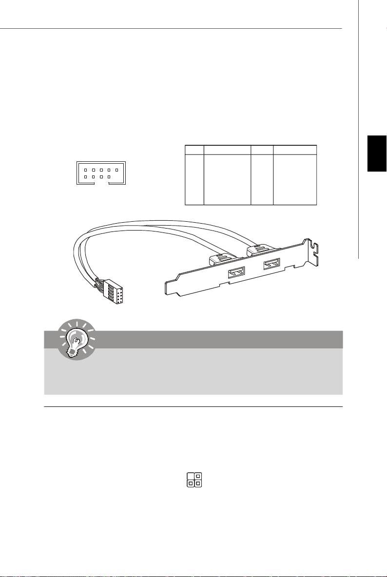
USB Vorderanschluss: JUSB1/ JUSB2
Dieser Anschluss entspricht den Richtlinien des Intel® I/O Connectivity Design Guide.
Er ist bestens geeignet, Hochgeschwindigkeits- USB- Peripheriegeräte anzuschließen,
wie z.B. USB Festplattenlaufwerke, Digitalkameras, MP3-Player, Drucker,
Modems und ähnliches.
Polzuweisung
JUSB1/ JUSB2
2
1
10
9
PIN SIGNAL PIN SIGNAL
1 VCC 2 VCC
3 USB0- 4 USB15 USB0+ 6 USB1+
7 GND 8 GND
9 Key (no pin) 10 NC
USB 2.0 Slotblech
Wichtig
Deutsch
Bitte beachten Sie, dass Sie die mit VCC (Stromführende Leitung) und GND
(Erdleitung) bezeichneten Pins korrekt verbinden müssen, ansonsten kann
es zu Schäden kommen.
GreenPower Genie Anschluss: JSMB1
Dieser Anschluss wird für das optionale GreenPower Genie verwendet. Weitere
Informationen über den Einsatz des optionalen GreenPower Genie entnehmen Sie
bitte dem GreenPower Genie Handbuch.
1
2
JSMB1
De-21
Page 69
MS-7520 Mainboard
Tasten
Nachfolgend werden die Funktion der neuen Tasten des Mainboard (optinoal) erläutert.
Ein-/Ausschalter: POWER1
Dieser Ein-/ Ausschalter verwendet, um das System ein- und auszuschalten. Drücken
Sie diese Taste, um das System ein- bzw. auszuschalten. Die Taste leuchtet nach
dem Systemstrom angeschaltet und das Tastelicht ausschaltet wenn das System
stromlos ist.
POWER1
Reset-Taste: RESET1
Diese Reset-Taste wird verwendet, um das System zurückzusetzen. Drücken Sie
diese Taste, um das System zurückzusetzen. Die Taste leuchtet wenn das System im
Status S0 ist.
RESET1
D-LED2 Menuänderung Taste: DLED2
Hier können Sie das Anzeige-Elemente des Boards auf dem D-LED2-Panel ändern.
Drücken Sie die Taste, um das Menü auf D-LED2-Panel ändern. Beziehen Sie sich den
Schnelleinstieg D-LED2 für mehr Details und Verbräuche.
DLED2
De-22
Page 70

Steckplätze
Der PCI Express-Steckplatz unterstützt eine Erweiterungskarte mit der PCI ExpressSchnittstelle.
Der PCI Express 2.0 x16-Steckplatz unterstützt eine Transferrate von bis zu 8.0
GB/s.
Der PCI Express 2.0 x4 -Steckplatz unterstützt eine Transferrate von bis zu 2.0
£įGB/s.
Der PCI Express x1 -Steckplatz unterstützt eine Transferrate von bis zu 250 MB/s.
Schwarze PCI Express x16 Steckplätze unterstützen
bis zu die Geschwindigkeit PCI Express 2.0 x16
(PCI_E2 & PCI_E4)
PCI Express x1 Steckplätze unterstützen bis
zu die Geschwindigkeit PCI Express x1
(PCI_E1 & PCI_E3)
Blau PCI Express x16 Steckplatz unterstützt bis
zu die Geschwindigkeit PCI Express 2.0 x4
(PCI_E5)
Deutsch
Wichtig
Das Mainboard unterstützt die ATI CrossFireXTM Technologie mit zwei
schwarze PCIEx16-Steckplätze und 3-Way CrossFireXTM mit alle drei PCIE
x16-Steckplätze.
De-23
Page 71

MS-7520 Mainboard
PCI (Peripheral Component Interconnect) Slot
Der PCI-Steckplatz kann LAN-Karten, SCSI-Karten, USB-Karten und sonstige
Zusatzkarten aufnehmen, die mit den PCI-Spezifikationen konform sind.
32-Bit PCI Steckplatz
Wichtig
Achten Sie darauf, dass Sie zuerst das Netzkabel aus der Steckdose
herausziehen, bevor Sie eine Erweiterungskarte installieren oder entfernen.
Denken Sie bitte auch daran die Dokumentation der Erweiterungskarte zu
lesen, um notwendige Hardware- oder Softwareeinstellungen fur die
Erweiterungskarte wie z.B. Jumper-, Schalter- oder BIOS-Einstellungen
vorzunehmen.
PCI Interrupt Request Routing
Eine IRQ (Interrupt Request; Unterbrechungsanforderung)-Leitung ist eine
Hardwareleitung, über die ein Gerät Unterbrechungssignale zu dem Mikroprozessor
schicken kann. Die PCI IRQ-Pole werden in der Regel mit dem PCI-Bus-Polen wie folgt
verbunden
Folge 1 Folge 2 Folge 3 Folge4
PCI Steckplatz 1 INT A# INT B# INT C# INT D#
PCI Steckplatz 2 INT B# INT C# INT D# INT A#
De-24
Page 72

Schalter
Hardware Übertaktung des Grundtakt Steckbrücke: CPU_CLK1
Übertaken den Grundtakt, um die Prozessorfrequenz erhöhen durch das Andern die
Steckbrücke. Folgen Sie die Anleitungen zur Einstellung Grund-Takt.
ON
123
133 MHz (default)
ON
123
166 MHz 200 MHz
ON
123
Wichtig
1. Stellen bitte Sie sicher, dass Sie schalten die System aus bevor Sie die
Steckbrücke ändern.
2. Die Ü bertaktung behavior hängt von die Systemkonfiguration (Speichers-
fähigkeit, Thermal-Auflösung...usw) ab, und es wird nicht garantiert.
3. Während des Start kann die HW-Übertaktung die Instabilitat oder der
Absturz verursachen, dann stellen Sie den Schalter zur
Standardeinstellung zurück.
4. Sie können auch übertakten, indem Sie BIOS einstellen. Die Übertaktung
des BIOS kann den Absturz während der Aufladung auch verursachen.
Und neu starten Sie das System 3mal, um die BIOS-Standardeinstellung
zurückzuspeichern. Fur mehr Details beziehen Sie sich das auf BIOSKapitel.
Deutsch
De-25
Page 73
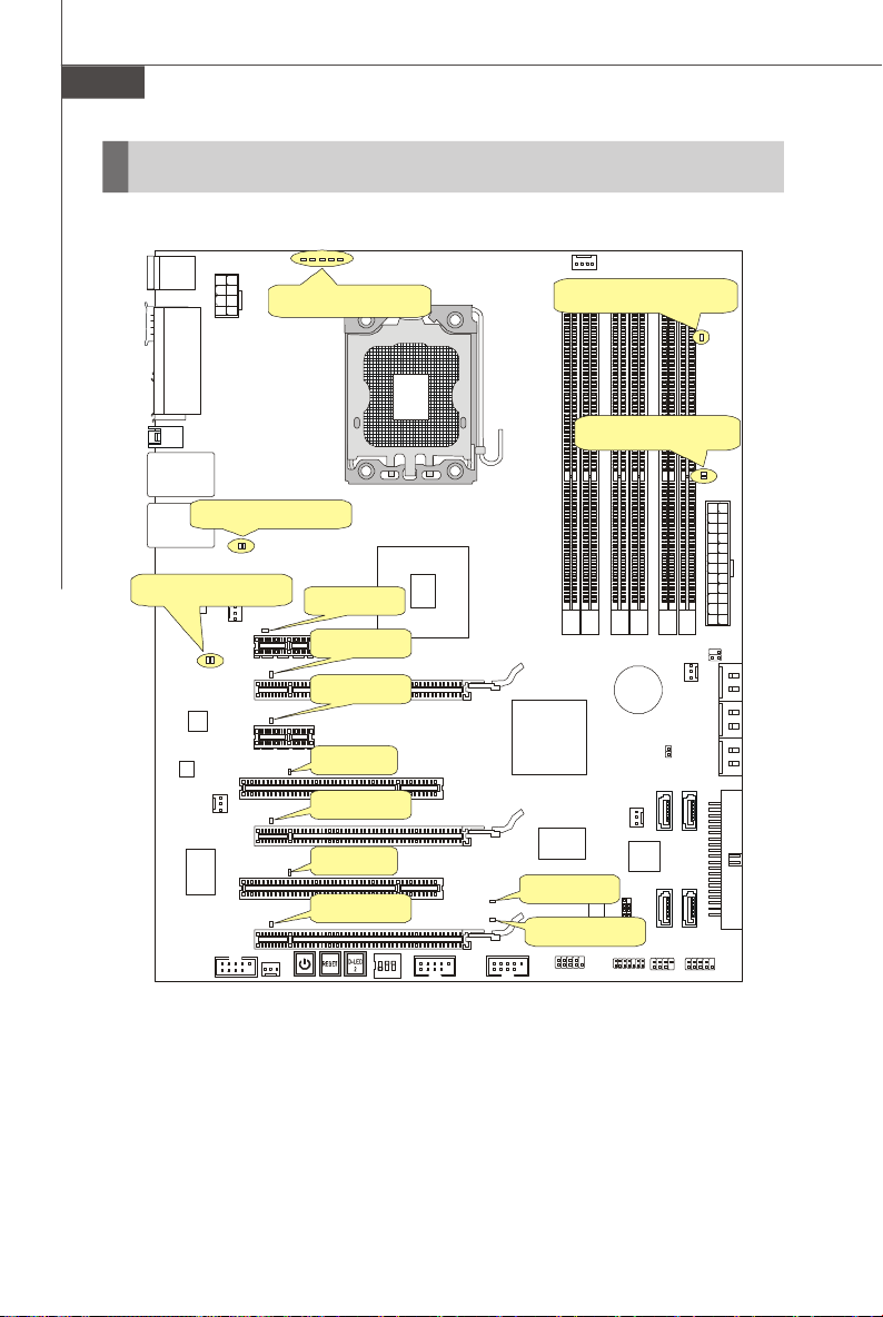
MS-7520 Mainboard
DDR Phase LEDs
DIMM warning LED
ON
LED Statusdikatoren
CPU Phase LEDs
QPI Phase LEDs
IOH Phase LEDs
PCIE LED
PCIE LED
PCIE LED
PCI LED
PCIE LED
PCI LED
Power LED
PCIE LED
Standby LED
123
De-26
Page 74

Name Status
CPU Phase LEDs 6 (5/ 4/ 3/ 2/ 1) LEDs leuchten je nach CPU-Belastung der
6 (5/ 4/ 3/ 2/ 1) Phasen blau, abhängig von der System
oder BIOS Eistellung
QPI Phase LEDs 2 (1) LEDs leuchten je nach QPI-Belastung der 2 (1)
Phasen blau, abhängig von der System oder BIOS
Eistellung.
IOH Phase LEDs 2 (1) LEDs leuchten je nach IOH (North Bridge) -
Belastung der 2 (1) Phasen blau, abhängig von der
System oder BIOS Eistellung.
DDR Phase LEDs 2 (1) LEDsleuchten je nach Speicher -Belastung der 2 (1)
Phasen blau, abhängig von der System oder BIOS
Eistellung.
PCI E LEDs Leuchtet blau, wenn der PCIE Slot betriebsbereit ist.
PCI LEDs Leuchtet blau, wenn der PCI Slot betriebsbereit ist.
Strom LED Leuchtet gr ün, wenn das System eingeschaltet und
betriebsbereit ist (S0/S1).
Bereitschaft LED Leuchtet orange, wenn das System auf Bereitschaft
(Stand-By) (S3/S4/ S5) ist.
DIMM Warnung LED Leuchtet rot, wenn der Speicher falsch eingebaut
wurde.
Deutsch
Wichtig
Durch Installation der “Green Power Center” Software haben Sie die
Möglichkeit, die Phasen (und somit die LEDs) zu- oder abzuschalten.
Alternativ können Sie die Einstellung ebenfalls im BIOS (Green Power Menu)
vornehmen.
De-27
Page 75

MS-7520 Mainboard
BIOS Setup
Dieses Kapitel enthält Informationen über das BIOS Setup und ermöglicht es Ihnen, Ihr
System optimal auf Ihre Anforderungen einzustellen. Notwendigkeit zum Aufruf des
BIOS besteht, wenn:
* Während des Bootvorgangs des Systems eine Fehlermeldung erscheint und Sie
zum Aufruf des BIOS SETUP aufgefordert werden.
* Sie die Werkseinstellungen zugunsten individueller Einstellungen ändern wollen.
Wichtig
1.Die Menüpunkte jeder BIOS Kategorie, die in diesem Kapitel beschrieben
wird, werden permanent auf den neuesten Stand gebracht, um die
Systemleistung zu verbessern. Aus diesem Grunde kann die Beschreibung
geringfügig von der aktuellsten Version des BIOS abweichen und sollte
dementsprechend lediglich als Anhaltspunkt dienen.
2. Während des Hochfahrens, wird die BIOS Version in der ersten Zeile nach
dem Hochzählen des Speichers angezeigt, üblicherweise im Format dieses
Beispiels:
Die erste Stellen den BIOS-Hersteller bezeichnet, dabei gilt A = AMI, W =
AWARD, und P = PHOENIX.
2te - 5te Stelle bezeichnen die Modelnummer.
6te Stelle bezeichen den Chipsatzhersteller, A = AMD, I = Intel, V = VIA, N =
Nvidia, U = ULi.
7te - 8te Stelle beziehen sich auf den Kunden, MS=alle Standardkunden.
V1.0 bezieht sich auf die BIOS Version.
101808 bezeichnet das Datum der Veröffentlichung des BIOS.
A7520IMS V1.0 101808 wobei:
De-28
Page 76

Aufruf des BIOS Setups
Nach dem Einschalten beginnt der Computer den POST (Power On Self Test Selbstüberprüfung nach Anschalten). Sobald die Meldung unten erscheint, drücken
Sie die Taste <Entf>(<Del>) um das Setup aufzurufen.
Press DEL to enter SETUP
Wenn die Nachricht verschwindet, bevor Sie reagieren und Sie möchten immer noch
ins Setup, starten Sie das System neu, indem Sie es erst AUS- und danach wieder
ANSCHALTEN, oder die “RESET”-Taste am Gehäuse betätigen. Sie können das Sys-
tem außerdem neu starten, indem Sie gleichzeitig die Tasten <Strg>,<Alt> und <Entf>
drücken (bei manchen Tastaturen <Ctrl>,<Alt> und <Del>).
Hilfe finden
Nach dem Start des Setup Menüs erscheint zuerst das Hauptmenü.
Hauptmenü
Das Hauptmenü listet Funktionen auf, die Sie ändern können.
Sie können die Steuertasten (↑↓ ) verwenden, um einen
Menüpunkt auszuwählen. Die Online-Beschreibung des
hervorgehobenen Menüpunktes erscheint am unteren
Bildschirmrand.
Untermenüs
Wenn Sie an der linken Seite bestimmter Felder ein Dreieckssymbol finden (wie
rechts dargestellt), bedeuted dies, dass Sie über das entsprechende Feld ein
Untermenü mit zusätzlichen Optionen aufrufen können. Durch die Steuertasten (↑↓
)önnen Sie ein Feld hervorheben und durch Drücken der Eingabetaste <Enter> in das
Untermenü gelangen. Dort können Sie mit den Steuertasten Werte eingeben und
navigieren. Durch Drücken von <Esc > kommen Sie zurü ck ins Hauptmenü .
Deutsch
Allgemeine Hilfe <F1>
Das BIOS Setup verfügt über eine Allgemeine Hilfe (General Help). Sie können diese
aus jedem Menü einfach durch Drücken der Taste <F1> aufrufen. Sie listet die Tasten
und Einstellungen zu dem hervorgehobenen Menüpunkt auf. Um die Hilfe zu verlassen,
drücken Sie <Esc>.
De-29
Page 77

MS-7520 Mainboard
Das Hauptmenü
Nachdem Sie das AMI® oder AWARD® BIOS CMOS Setup Utility, aufgerufen haben,
erscheint das Hauptmenü. Es weist zehn Setup- Funktionen und zwei Arten das
Menü zu verlassen auf. Verwenden Sie die Pfeiltasten, um im Menü zu navigieren
und drücken Sie die Eingabetaste (<Enter>), um ein Untermenü aufzurufen.
Standard CMOS Features
In diesem Menü können Sie die Basiskonfiguration Ihres Systems anpassen, so z.B.
Uhrzeit, Datum usw.
Advanced BIOS Features
Verwenden Sie diesen Menüpunkt, um weitergehende Einstellungen an Ihrem System vorzunehmen.
Integrated Peripherals
Verwenden Sie dieses Menü, um die Einstellungen für in das Board integrierte
Peripheriegeräte vorzunehmen.
Power Management Setup
Verwenden Sie dieses Menü , um die Einstellungen für die Stromsparfunktionen
vorzunehmen.
H/W Monitor
Dieser Eintrag zeigt den generellen Systemstatus.
Green Power
Verwenden Sie dieses Menü, um Einstellungen der Stromversorgung vorzunehmen..
BIOS Setting Password
Verwenden Sie dieses Menü, um das Kennwort für das BIOS einzugeben.
Cell Menu
Hier können Sie Ihre Einstellungen zur Kontrolle von Frequenz und Spannung und zur
Übertaktung vornehmen.
User Settings
Hier können Sie Ihre Einstellungen zum/ vom CMOS für BIOS abspeichern/ laden.
M-Flash
In diesem Menü können Sie das BIOS vom Speicher-Antrieb abtasten/ aufblinken
(nur FAT/ FAT32 Format).
Load Fail-Safe Defaults
In diesem Menü können Sie eine stabile, werkseitig gespeicherte Einstellung des
BIOS Speichers laden.
Load Optimized Defaults
In diesem Menü können Sie die BIOS-Voreinstellungen laden, die der
Mainboardhersteller zur Erzielung der besten Systemleistung vorgibt.
Save & Exit Setup
Abspeichern der BIOS-Änderungen im CMOS und verlassen des BIOS.
Exit Without Saving
Verlassen des BIOS´ ohne Speicherung, vorgenommene Ä nderungen verfallen.
De-30
Page 78

Wenn Sie das BIOS Dienstprogramm öffnen, folgen Sie den untenstehenden
Anweisungen.
1. Laden der optimalen Voreinstellung : Verwenden Sie die Steuerschlüssel (
↑↓ ), um dem Laden der optimalen Voreinstellung zu wählen und drücken Sie
auf <Eingabe>. Dann erscheint die folgende Meldung:
Drücken Sie auf [OK] und <Enter>, um die im Werk eingestellten Standardwerte
für eine optimale Systemleistung zu laden.
2. Die Datum/Zeit Einstellung : W ählen Sie die “Standard-CMOS Features” vor
und drücken Sie <Eingabe> um das Standard-CMOS Features-Menü zu wählen.
Passen Sie nun die Felder “Datum” und “Zeit” an.
3. Abspeichern u. Beenden der Einstellung: Verwenden Sie die Steuerschlüssel
(↑↓ ), um dem Abspeichern u. Beenden der Einstellungen zu wählen und
drücken Sie auf <Eingabe>. Es erscheint folgende Meldung:
Deutsch
Drücken Sie auf [OK] und <Enter>, um die (neuen) Einstellungen zu speichern
und das BIOS Setup zu verlassen.
Wichtig
Die Konfiguration oben dienen nur generellen Zwecken. Wenn Sie detaillierte
BIOS- Einstellungen benötigen, dann sehen Sie bitte das Handbuch in
Englischer Sprache auf der MSI Website ein.
De-31
Page 79

MS-7520 Mainboard
4. Cell Menu Introduction : Das Menü ist für den weiteren Benutzer, der die
Hauptplatine übertakten mögen.
Wichtig
Nur wenn Sie mit dem Chipsatz vertraut sind, können Sie die Einstellung
ändern .
Current Core / DRAM / QPI Frequency
Zeigt die derzeitige Frequenz der CPU/ Speicher. Nur Anzeige.
De-32
Page 80

CPU Specifications
Drücken Sie die Eingabetaste <Enter>, um das folgende Untermenü aufzurufen.
Das Untermenü zeigt die Informationen angebrachter CPU an.
CPU Technology Support
Drücken Sie die Eingabetaste <Enter>, um das folgende Untermenü aufzurufen.
Das Untermenü zeigt die Technologien an, die die angebrachte CPU stützt.
D.O.T. Kontrolle
Dynamic Overclocking Technology (D.O.T) ist die automatische Ü bertaktungsfunktion,
die in MSITM’s neu entwickelter CoreCell
TM
Technologie enthalten ist. Sie dient zur
Feststellung des Auslastungsgrades der CPU, während diese Programme abarbeitet,
und passt die CPU-Frequenz automatisch an. Stellt das Motherboard fest, dass die
CPU Programme ausführt, beschleunigt es automatisch die CPU und erlaubt so eine
flüssige und schnellere Ausführung. Ist die CPU ohne Last oder nur wenig ausgelastet,
werden statt dessen die Voreinstellungen wieder hergestellt. Üblicherweise kommt
die Technologie der dynamischen Übertaktung nur zum Einsatz, wenn große
Datenmengen bewältigt werden müssen, wie das bei 3D Spielen oder der
Videoverarbeitung der Fall ist. In diesen Fällen ist es notwendig, die CPU -Frequenz
zu erhöhen, um die Gesamtleistung des Systems zu erhöhen. Die möglichen
Einstellungen sind.
Wichtig
Obgleich Dynamic Overclocking Technology stabiler ist als manuelles
Übertakten, ist es dennoch grundsätzlich riskant. Es ist empfehlenswert zuerst
sicher zu stellen, dass Ihre CPU eine regelmäßige Übertaktung verträgt. Sollten
Sie feststellen, dass Ihr PC instabil erscheint oder ohne erkennbaren Grund
Neustarts durchführt, it es besser, die dynamische Übertaktung abzuschalten
oder aber eine niedrigere Übertaktungsstufe zu wählen. Im Übrigen ist zu
erwähnen, dass Sie die Dynamische Übertaktung zuerst abschalten mussen,
bevor Sie Ihr System manuell übertakten.
Deutsch
Intel EIST
Die erhöhte Intel SpeedStep Technologie erlaubt Ihnen, das Leistungsgrad des
Mikroprozessors einzustellen, ob der Computer auf Batterie oder Wechselstrom läuft.
Wenn Sie das CPU Ratio zu justieren möchten, lautet die Einstellung auf “Disabled
(ausgeschaltet)”. Nur Sie brachten die CPU an, das Speedstep Technologie stützen.
Intel C-STATE tech
C-Status ist ein Stromsparfunktionalität-Zustand, der der Strom des Prozessor
während des Leerlaufs erheblich verringert. Es wird erscheinen, wenn der CPU der
C-Status Technologie unterstützt.
De-33
Page 81

MS-7520 Mainboard
Base Clock (MHz)
Hier können Sie den CPU Grundtakt (in MHz) angeben. Sie können das CPU übertakten,
indem Sie diesen Wert justieren. Bitte beachten Sie dass die Ü bertaktung wird
garantiert nicht.
Intel Turbo Boost tech
Das Untermenü erscheint, wenn Sie eine CPU anbringen, die die Intel Turbo Boost
Technologie aufnehmt. Und hier können Sie die Intel Turbo Boost Technologie aktiviert/
deaktiviert.Es kann die Prozessorfrequenz stark dynamisch ersteigen, wenn
Anwendungen mehr Leistung verlangen und TDP Durchfahrtshöhe besteht. Es kann
nachlose Stromskalierbarkeit (Dynamically scale up, Speed-Step Down) auch liefern.
Es ist die Intel eben Technologie innerhalb CPU i7.
Turbo Boost Tech Config
Das Untermenü erscheint, wenn Sie eine CPU anbringen, die die Intel Turbo Boost
Technologie aufnehmt. Drücken Sie die Eingabetaste <Enter>, um das folgende
Untermenü aufzurufen.
Turbo Ratio Limit Program
Hier können Sie das Turbo Ratio Limit Program aktiviert/ deaktiviert. Lautet die
Einstellung auf [Enabled] (eingeschaltet), aktiviert die folgenden Felder, und
festsetzt den jede Ratio des CPU.
1/2/3/4-Core Ratio Limit
Hier können Sie den Ratio des CPU anpassen.
TDC Limit Override
Lautet die Einstellung auf [Enabled] (eingeschaltet), aktiviert das Feld des TDC
Limit Value, und festsetzt den Wert des CPU TDC.
TDC Limit value (A)
Hier können Sie der Wert (Ampere) des CPU TDC.
TDP Limit Override
Lautet die Einstellung auf [Enabled] (eingeschaltet), aktiviert das Feld des TDP
Limit Value, und festsetzt den Wert des CPU TDP.
TDP Limit value (W)
Können Sie hier den Wert (Watt) des CPU TDP anpassen.
Adjusted Core Frequency (MHz)
Gibt der verstellt Frequenz des CPU (Grundtakt x Ratio). Nur Anzeige.
QPI Configuration
Drücken Sie die Eingabetaste <Enter>, um das folgende Untermenü aufzurufen.
QPI Links Speed
Hier können Sie die QPI Link Geschwindigkeittyp auswählen .
De-34
Page 82

QPI Frequency
Hier können Sie die QPI Frequenz auswählen.
Memory-Z
Drücken Sie die Eingabetaste <Enter>, um das folgende Untermenü aufzurufen.
DIMM1~6 Memory SPD Information
Drücken Sie die Eingabetaste <Enter>, um das folgende Untermenü aufzurufen.
Das Untermenü zeigt die Informationen angebrachtes Speicheran.
Advance DRAM Configuration
Drücken Sie die Eingabetaste <Enter>, um das folgende Untermenü aufzurufen.
1N/2N Memory Timing
Können Sie hier die DRAM Timing angeben. Legt die SDRAM Kommandorate fest.
Die Einstellung 1N lässt den SDRAM Signal Kontroller mit einem 1N ((Taktzyklus)
laufen. Bei 2N läuft er mit zwei Zyklen. 1N ist schneller als 2N.
CAS# Latency (CL)
Hier wird die Verzögerung im Timing (in Taktzyklen) eingestellt, bevor das SDRAM
einen Lesebefehl nach dessen Erhalt auszuführen beginnt.
tRCD
Wenn DRAM erneuert wird, werden Reihen und Spalten separat adressiert.
Dies gestattet es, die Anzahl der Zyklen und der Verzogerung im Timing
einzustellen, die zwischen den CAS und RAS Abtastsignalen liegen, die
verwendet werden, wenn der DRAM beschrieben, ausgelesen oder aufgefrischt
wird. Eine hohe Geschwindigkeit führt zu höherer Leistung, während langsamere
Geschwindigkeiten einen stabileren Betrieb bieten.
tRP
Legt die Anzahl der Taktzyklen fest, die das Reihenadressierungssignal (Row
Address Strobe - RAS) für eine Vorladung bekommt. Wird dem RAS bis zur
Auffrischung des DRAM nicht genug Zeit zum Aufbau seiner Ladung gegeben,
kann der Refresh unvollständig ausfallen und das DRAM Daten verlieren. Dieser
Menüpunkt ist nur relevant, wenn synchroner DRAM verwendet wird.
Deutsch
tRAS
Stellt die Zeit der RAS Lese- und Schreibzugriffe ein.
Advanced Memory Setting
Die Einstellung [Auto] ermoglicht dem vorgerückten Speicher-Timing, die von
BIOS automatisch festgestellt wird. Lautet die Einstellung [Manual], können Sie
hier die vorgerückte Speicher-Timing angeben.
Extreme Memory Profile
Hier können Sie das Extreme-Memory-Profile (X.M.P.) aktiviert/ deaktiviert. Für weitere
Informationen beziehen Sie in offizielle Website des Intel.
De-35
Page 83

MS-7520 Mainboard
Memory Ratio
Hier können Sie die Speicher-Multiplikator.
Adjusted DRAM Frequency (MHz)
Gibt den geänderten Frequenz-Wert des DDR Speicher an. Nur Anzeige.
ClockGen Tuner
Drücken Sie die Eingabetaste <Enter>, um das folgende Untermenü aufzurufen.
CPU / PCI Express Amplitude Control
Gestattet die Wahl der CPU-Takt oder PCI-E Takt.
CPU CLK Skew/ IOH CLK Skew
Gestattet die Wahl der CPU/ North-Bridge Chipsatztakt,durch Einstellung eines
höheren CPU Taktes.
Adjust PCI Frequency (MHz)
Gestattet die Wahl der PCI-E Frequenz (in MHz).
Adjust PCI-E Frequency (MHz)
This field allows you to select the PCIE frequency (in MHz).
Auto Disable DRAM/PCI Frequency
Lautet die Einstellung auf [Enabled] (eingeschaltet), deaktiviert das System die
Taktung leerer PCI Sockel, um die Elektromagnetische Störstrahlung (EMI) zu
minimieren.
CPU Voltage (V)/ QPI Voltate (V))/ CPU PLL Voltage (V)/ DRAM Voltage (V)/
DDR_VREF_CA_A (V)/ DDR_VREF_CA_B (V)/ DDR_VREF_CA_C (V)/
DDR_VREF_DQ_A (V)/DDR_VREF_DQ_B (V), DDR_VREF_DQ_C (V)/ IOH Voltage
(V), ICH Voltage (V)
Diese Option bietet bietet die Moglichkeit, die Spannung der CPU, des Speichers und
des QPI sowie des Chipsatz anzupassen.
For CPU Voltage:
Dieser Eintrag ermoglicht innerhalb eines Bereiches die CPU Spannung zu ändern /
anzupassen. Lesen Sie dazu die Standard CPU-Spannung “CPU Vcore” auf der “H/W
Monitor” BIOS Seite nach. Bitte beachten Sie, dass die CPU Spannung je nach
eingesetzter CPU variieren kann.
For QPI Voltage:
Dieser Eintrag ermöglicht innerhalb eines Bereiches die QPI Spannung zu ändern /
anzupassen. Die Standardspannung liegt zwischen 1.1V und 1.22V und varriiert, je
nach eingesetzter CPU. Im Green Power Center haben Sie die Möglichkeit, die QPI
Spannung zu erhalten.
For DRAM Voltage:
Laut Intel Spezifikationen kann eine DRAM Spannung von 1,65V und mehr die CPU
beschädigen. Bitte achten Sie beim Einstellen des Wertes darauf, unter dem Wert der
Intel Vorgaben zu bleiben. Im Green Power Center haben Sie die Möglichkeit, die
DRAM Spannung zu erhalten.
De-36
Page 84

Spread Spectrum
Pulsiert der Taktgenerator des Motherboards, erzeugen die Extremwerte (Spitzen)
der Pulse EMI (Elektromagnetische Interferenzen). Die Spread Spectrum Funktion
reduziert die erzeugten EMI, indem die Pulse so moduliert werden, das die Pulsspitzen
zu flacheren Kurven reduziert werden.
Wichtig
1. Sollten Sie keine Probleme mit Interferenzen haben, belassen Sie es bei
der Einstellung [Disabled] (ausgeschaltet), um bestmögliche
Systemstabilität und -leistung zu gewährleisten. Stellt für sie EMI ein
Problem dar, wählen Sie die gewünschte Bandbreite zur Reduktion der
EMI.
2. Je größer Spread Spectrum Wert ist, desto größer nimmt der EMI ab, und
das System wird weniger stabil. Bitte befragen Sie Ihren lokalen EMI
Regelung zum meist passend Spread Spectrum Wert.
3. Denken Sie daran Spread Spectrum zu deaktivieren, wenn Sie übertakten,
da sogar eine leichte Schwankung eine vorübergehende Taktsteigerung
erzeugen kann, die gerade ausreichen mag, um Ihren übertakteten
Prozessor zum einfrieren zu bringen.
Deutsch
De-37
Page 85

MS-7520 Mainboard
Software-Information
Die im Mainboard-Paket enthaltene CD enthält alle notwendigen Treiber. Um die Instal-
lation automatisch laufen zu lassen, klicken Sie einfach den Treiber oder Utiltiy und
folgen Sie dem Pop-Up Schirm, um die Installation durchzuführen. Der
Treibergebrauchs-CD enthält:
Treibermenü - das Treibermenü zeigt die vorhandenen Treiber. Aktivieren Sie den
Gebrauchsmenü - das Gebrauchsmenü zeigt die Software-Anwendungen der die
WebSite Menü - das Website Menü zeigt die betreffende Website.
Besuchen Sie bitte die MSI Website, um die neuesten Treiber und BIOS für
bessere System Leistung zu erhalten.
gewünschten Treiber.
Mainboard Unterstützungen.
Wichtig
De-38
Page 86

ECLIPSE
Guide d’utilisation
Français
Français
Fr-1
Page 87
Carte mère MS-7520
Spécifications
Processeurs Supportés
- Intel® i7 processeurs dans le paquet LGA1366
(Pour plus d’informations sur le CPU, veuillez visiter
http://global.msi.com.tw/index.php?func=cpuform2)
QPI Supporté
- Jusqu’à 6.4 GT/s
Chipset
- IOH : chipset Intel® X58
- ICH : chipset Intel® ICH10R
Mémoire support ée
- 6 DDR3 DIMMs supportent la vitesse du DDR3 1333/ 1066/ 800
DRAM (Dimension de Mémoire 24GB Max)
- Supporte DRAM de dimensions de 1Gb/ 2Gb/ 4Gb
- Supporte x8/ x16 data lignes par chaque DRAM puce
- Supporte jusqu’au mode de 3 canaux
(Pour plus d’informations sur les composants compatibles, veuillez
visiter http://global.msi.com.tw/index.php?func=testreport)
LAN
- Supporte 2 PCIE LAN 10/100/1000 Fast Ethernet par Realtek
8111C
Audio
- X-Fi Xtreme Audio Carte
- 24-bit/ 96 KHz audio qualité
- 100dB SNR clarté
- Jusqu’à 7.1 ch EAX 5.0 Surround Sound
IDE
- 1 port IDE par JMicron JMB363
- Supporte le mode Ultra DMA 66/100/133
- Supporte les modes d’opé ration PIO, Bus Master
SATA
- 6 ports SATA (SATA1~6) par ICH10R
- 4 ports SATA (SATA7~10 supportent seulement les périphériques de
stockage) par JMicron JMB322
- 2 ports E-SATA par JMicron JMB362
- Supporte le stockage et un taux de transfert jusqu’à 3 Gb/s
RAID
- SATA1~6 supportent Intel Matrix Storage Technology (AHCI/
RAID 0/ 1 / 5/ 10) par ICH10R
- 2 ports E-SATA sur le panneau arrière supportent le mode RAID 0/
1 et JBOD par JMicron JMB362
Fr-2
Page 88
Matériel RAID
- SATA7 et SATA8 supportent le mode RAID 0/ 1 et JBOD par 1er
JMicron JMB322
- SATA9 et SATA10 supportent le mode RAID 0/ 1 et JBOD par
2ème JMicron JMB322
1394
- Supporte 2 ports 1394 (arrière*1, avant*1) par VIA VT6308P
Connecteurs
Panneau arrière
- 1 port souris PS/2
- 1 port clavier PS/2
- 1 port 1394
- 2 ports eSATA
- 8 ports USB 2.0
- 2 jacks LAN
- 1 bouton d’effacement CMOS
Connecteurs intégrés
- 2 connecteurs USB 2.0
- 1 connecteur 1394
- 1 connecteur châssis intrusion
- 1 connecteur de port sérial
- 1 connecteur de TPM Module
- 1 connecteur de D-LED2 panneau
TPM
- Supporte TPM
Slots
- 3 slots PCI Express gen2 x16, 2 slots Noirs PCIE x16 (PCI_E2 et
PCI_E4) supportent la vitesse jusqu’à PCIE x16, 1 slot Bleu PCIE
x16 (PCI_ E5) supporte la vitesse jusqu’à PCIE x4)
- 2 slots Noirs PCI Express x1
- 2 slots PCI, supportent l’interface bus PCI 3.3V/ 5V
Dimension
- ATX (30.5cm X 24.5cm)
Montage
- 9 trous de montage
Français
Fr-3
Page 89

Carte mère MS-7520
ON
Guide rapide des composants
Back Panel,
Fr-14
PCI_E,
Fr-23
SYSFAN1,
Fr-18
PCI,
Fr-24
J1394_1,
Fr-18
SYSFAN4, Fr-18
JPWR2, Fr-13
SYSFAN5, Fr-18
CPU, Fr-5
123
CPU_CLK1,Fr-25
DLED2, Fr-22
RESET1, Fr-22
POWER1, Fr-22
SYSFAN2, Fr-18
CPUFAN, Fr-18
JCOM1, Fr-19
JUSB1~2, Fr-21
JTPM1, Fr-20
DDR3, Fr-9
JPWR1, Fr-13
SYSFAN3, Fr-18
JSMB1, Fr-21
SATA, Fr-17
JCI1, Fr-20
IDE1, Fr-16
SATA, Fr-17
JDLED2, Fr-20
JFP2, JFP1,
Fr-19
Fr-4
Page 90

Processeur : CPU
Quand vous installez le CPU, veuillez vous assurer que l’unité centrale est
équipée d’un ventilateur de refroidissement attaché sur le dessus pour
éviter la surchauffe. Si vous n’en avez pas, contactez votre revendeur pour en
acheter et installez les avant d’allumer votre ordinateur.
Pour plus d’informations sur le CPU, veuillez visiter http://global.msi.com.tw/index.
php?func=cpuform2
Important
Surchauffe
La surchauffe endommage sérieusement l’unité centrale et le système.
Assurez-vous toujours que le ventilateur de refroidissement fonctionne
correctement pour protéger l’unité centrale contre la surchauffe. Assurez-
vous d’appliquer une couche d’enduit thermique (ou film thermique) entre
l’unité centrale et le dissipateur thermique pour améliorer la dissipation de
la chaleur.
Remplacement de l’unité centrale
Lorsque vous remplacez l’unité centrale, commencez toujours par couper
l’alimentation électrique de l’ATX ou par débrancher le cordon d’alimentation
de la prise mise à la terre pour garantir la sécurité de l’unité centrale.
Overclocking
Cette carte mère supporte l’overclocking. Néanmoins, veuillez vous assurer
que vos composants soient capables de tolérer ces configurations anormales,
lors d’overclocking. Tout envie d’opérer au dessus des spécifications du
produit n’est pas recommandé. Nous ne garantissons pas les dommages
et risques causés par les opérations insuffisantes ou au dessus des
spécifications du produit.
Français
Introduction du LGA 1366 CPU
La face de la galette à
contacts du LGA 1366 CPU.
Clé d’ alignement
Le triangle jaune est l’ indicateur du Pin 1. Le triangle jaune est l’ indicateur du Pin 1.
La surface du LGA 1366 CPU.
N’oubliez pas d’appliquer une
couche d’enduit thermique pour
améliorer la dissipation de la
chaleur.
Clé d’alignement
Fr-5
Page 91

Carte mère MS-7520
Installation du CPU et son ventilateur
Quand vous installez le CPU, veuillez vous assurer que l’unité centrale soit
équipée d’un ventilateur de refroidissement attaché sur le dessus pour
éviter la surchauffe. Méanmoins, n’oubliez pas d’appliquer une couche d’enduit
thermique sur le CPU avant d’installer le ventilateur pour une meilleure dissipation de
chaleur.
Suivez les instructions suivantes pour installer le CPU et son ventilateur correcement.
Une faute installation peut endommager votre CPU et votre carte mère.
1. Ouvrez le levier de charge.
2.Levez le levier et ouvrir le plateau
de chargement.
3. La douille du CPU possède une
couverture plastique qui protège la
contact. Avant d’installer le CPU,
toujours gardez-la pour protéger les
pins de la douille. Retirez cette
couverture de la face d’articulation
du levier (comme montre la flèche).
Fr-6
4.Après avoir confirmé la direction du
CPU pour joindre correctement,
déposez le CPU dans l’armature du
logement de douille. Faites attention
au bord de sa base. Notez qu’on
aligne les coins assortis.
Clé d’ alignement
Page 92

5.Inspectez visuellement si le CPU est
bien posé dans le douille. Sinon,
sortez verticalement le CPU pur et la
réinstallez.
6.Couvrez le plat de charge sur le
paquet.
Français
7.Abaissez le levier sur le plateau de
chargement, puis sécuriser
l’ensemble avec le mécanisme de
rétention.
8.Alignez les trous de la carte avec le
dissipateur thermique. Appuyez sur
le ventilateur jusqu’à ce que les clips
soient coincés dans les trous de la
carte mère.
Important
1.Comfirmez si votre ventilateur du CPU est fermement installé avant d’allumer
votre système.
2. Ne touchez pas les pins du CPU afin d’éviter tout dommage.
Fr-7
Page 93

Carte mère MS-7520
9. Appuyez sur les quatre crochets
afin de fixer le ventilateur.
10. Retournez la carte mère pour
s’assurer que le ventilateur est
correctement installé.
Carte mère
Interrupteur de
verrouillage
Crochet
Important
1. Lisez le statut du CPU dans le BIOS.
2. Quand le CPU n’est pas installé, toujours protectez vos pins de la douille
CPU avec le plastique de protection pour éviter tout dommage. (Montré dans
la Figure 1).
3. Les photos de la carte montrées dans cette section ne sont que pour une
démonstration de l’installation du CPU et son ventilateur. L’apparence de votre
carte mère peut varier selon le modèle que vous achetez.
Fr-8
Page 94

Mémoire
Installed
1
2
Ces slots de DIMM sont destinés à installer les modules de mémoire.
Pour plus d’informations sur les composants compatibles, veuillez visiter http://
global.msi.com.tw/index.php?func=testreport
DDR3
240-pin, 1.5V
48x2=96 pin
Règles de population de la mémoire
Veuillez vous référer aux illustrations suivantes pour les règles de population de la
mémorie.
Mode simple-canal
Quand vous n’avez qu’un seule module mémpoire, veuillez toujours l’insérer dans
DIMM_A0 d’abord (comme la façon 1 montré ci-dessous).
Mode double-canaux
Au mode double-canaux, les modules de mémoire peuvent tranmettre et recevoir les
données avec deux lignes bus de données sémultanément. L’activation du mode
double-canaux peut augmenter la performance. Quand vous avez deux modules de
mémoire, veuillez toujours les insérer dans DIMM_A0 et DIMM_B0 (comme la façon 2
montré ci-dessous).
72x2=144 pin
DIMM_A1
DIMM_A0
DIMM_B1
DIMM_B0
DIMM_C1
DIMM_C0
Français
DIMM_A1
DIMM_A0
DIMM_B1
DIMM_B0
DIMM_C1
DIMM_C0
Installé
Empty
Vide
Fr-9
Page 95

Carte mère MS-7520
3
4
5
6
Mode trois-canaux
En mode trois-canaux, les modules de mémoire peuvent transmettre et recevoir les
données avec trois lignes bus de données sémultanément. L’activation du mode
trois-canaux peut l’augmenter à la meuilleure performance du système. Quand
vous avez trois ou plus de modules de mémoire, veuillez toujours les insérer
comme les façons 3/ 4/ 5/ 6 (montré ci-dessous) afin d’obtenir la meilleure
performance.
DIMM_A1
DIMM_A0
DIMM_B1
DIMM_B0
DIMM_C1
DIMM_C0
DIMM_A1
DIMM_A0
DIMM_B1
DIMM_B0
DIMM_C1
DIMM_C0
DIMM_A1
DIMM_A0
DIMM_B1
DIMM_B0
DIMM_C1
DIMM_C0
DIMM_A1
DIMM_A0
DIMM_B1
DIMM_B0
DIMM_C1
DIMM_C0
Fr-10
Page 96
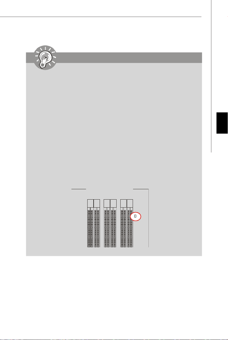
Important
DIMM_A1DIMM_A0DIMM_B1DIMM_C1DIMM_B0DIMM_C
0
-Les modules de mémoire DDR3 ne sont pas interchangeables par DDR2 et
vice versa. Vous devez toujours installer les modules de mémoire DDR3
dans les slots DDR3 DIMM.
-En mode trois-/ double- canaux, assurez-vous que vous installez les mod-
ules de mémoire du même type et de la même densité dans les slots DIMM
de canaux différents. Si les vitesses des modules de mémoire installés sont
différentes (ex. 1066 et 1333), le système détectera et opérera la vitesse
plus basse (1066) avec tous les modules de mémoire installés.
- Veuillez toujours installer les modules de mémoire du même type et de la
même densité dans les slots DIMM afin d’éviter tout dommage de la mémoire.
-Pour lancer avec succès votre ordinateur, insérez toujours tout d’abord les
modules de mémoire dans les DIMM_A0.
- A cause du développement de la ressource du chipset, la densité du système
sera détecté seulement jusqu’à 23+GB (non 24GB) quand chaque DIMM est
installé avec un module de mémoire de 4GB.
- Quand vous installez un incorrect module de mémoire (le SA2-pin du module
de mémoire se connecte à Terre) dans le DIMM_C0/C1, le LED à côté du
DIMM_C0 s’allumera en rouge pour vou rappeler. La position du LED est
montrée ci-dessous. Veuillez confirmer avec votre vendeur du module de
mémoire pour le troisième support du canal.
Français
Fr-11
Page 97
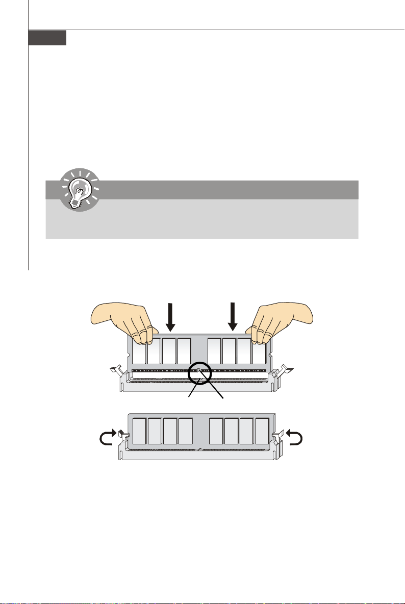
Carte mère MS-7520
Installation des modules de mémoire
1. Le module de mémoire possède une seule encoche en son centre et ne s’adaptera
que s’il est orienté de la manière convenable.
2. Insérez le module de mémoire à la verticale dans le slot du DIMM. Poussez-le
ensuite jusqu’à l’extrémité dorée du module de mémoire, soit profondément insérée
dans le slot du DIMM. Les clips en plastique situés de chaque côté du module va se
fermer automatiquement.
Important
Vous pourrez à peine voir l’extrémité dorée si le module de mémoire est
correctement inséré dans le slot du DIMM.
3. Vérifiez manuellement si la barrette mémoire a été verrouillée en place par les clips
du slot DIMM sur les côtés.
Fr-12
Volt
Encoche
Page 98

Connecteurs d’alimentation
Connecteur d’alimentation ATX 24-Pin : JPWR1
Ce connecteur vous permet de connecter l’alimentation ATX 24-pin.
Pour cela, assurez-vous que la prise d’alimentation est bien
positionnée dans le bon sens et que les goupilles soient alignées.
Enfoncez alors la prise dans le connecteur.
Vous pourvez aussi utiliser un alimentation 20-pin selon vos besoins.
Veuillez brancher votre alimentation d’énergie avec le pin 1 et le pin
13 si vous voulez utiliser l’alimentation ATX 20-pin (Référez-vous à
l’image à droite).
Dé finition de pins
PIN SIGNAL
13 +3.3V
14 -12V
15 GND
16 PS-ON#
17 GND
18 GND
19 GND
20 Res
21 +5V
22 +5V
23 +5V
24 GND
JPWR1
12
1
24
13
PIN SIGNAL
1 +3.3V
2 +3.3V
3 GND
4 +5V
5 GND
6 +5V
7 GND
8 PWR OK
9 5VSB
10 +12V
11 +12V
12 +3.3V
Connecteur d’alimentation ATX 12V : JPWR2
Le connecteur d’alimentation sert à fournir de l’alimentation au CPU.
Définition de pins
PINSIGNAL
1 GND
2 GND
3 GND
4 GND
PINSIGNAL
5 +12V
6 +12V
7 +12V
8 +12V
JPWR2
4
1
8
5
pin 13
pin 12
Français
Important
1. Veuillez vous assurer que tous les connecteurs sont connectés aux correctes
alimentations ATX pour garantir une opération stable de la carte mère.
2. L’alimentation de 450 watts (et plus) est fortement recommandée pour la
stabilité du système.
3. La connexion de l’alimentation ATX 12V doit être plus haut que 18A.
Fr-13
Page 99

Carte mère MS-7520
Panneau arrière
Ports USB
Souris
clavier
LAN
LAN
Port 1394
Ports eSATA
Bouton d’effacement CMOS
Ports USB
Ports USB
Souris/Clavier
Le standard connecteur de souris/clavier DIN de PS/2® est pour une souris ou un
clavier de PS/2®.
Port 1394
Le port IEEE1394 sur le panneau arrière fournit une connexion aux périphériques
IEEE1394.
Port USB
Le port USB (Universal Serial Bus) sert à brancher des périphériques USB tel que le
clavier, la souris, ou d’autre périphériques compatibles USB.
Port eSATAA
Le port eSATA port sert à attacher un disque dur externe eSATA.
Bouton d’effacement CMOS
Il y a un CMOS RAM intégré, qui possède un bloc d’alimentation alimenté par une
batterie externe, destiné à conserver les données de configuration du système.
Avec le CMOS RAM, le système peut lancer automatiquement le système d’exploitation
chaque fois qu’il est allumé. Si vous souhaitez effacer la configuration du système,
utilisez ce bouton pour effacer les données. Appuyez sur ce bouton pour effacer les
données.
Important
Veuillez vous assurer d’éteindre le système avant d’effacer les données CMOS.
Fr-14
Page 100

LAN
La prise standard RJ-45 LAN sert à la connexion
au réseau local (Local Area Network (LAN)). Vous
pouvez y relier un câble de réseau.
LED Couleur LED Statut Condition
Eteinte La connexion au ré seau LAN n’est pas établie.
Gauche Jaune Allumée (stable) La connexion au réseau LAN est établie.
Allumée (plus brillant et
clignotante)
Vert Eteinte
Droite Allumée
Orange Allumée
L’ ordinateur communique avec un autre ordinateur
sur le réseau local LAN.
Un dé bit de 10 Mo/sec est sélectionné.
Un débit de 100 Mo/sec est sélectionné.
Un débit de 1000 Mo/sec est sélectionné.
Vert / OrangeJaune
Français
Fr-15
 Loading...