

Page 1
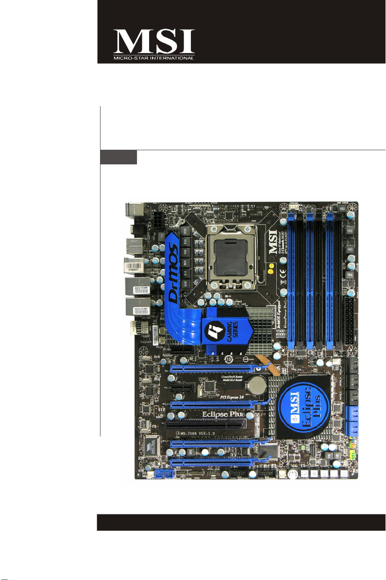
Eclipse Plus Series
MS-7566 (V1.X) Mainboard
G52-75661X3
i
Page 2

Copyright Notice
The material in this document is the intellectual property of MICRO-STAR
INTERNATIONAL. We take every care in the preparation of this document, but no
guarantee is given as to the correctness of its contents. Our products are under
continual improvement and we reserve the right to make changes without notice.
Trademarks
All trademarks are the properties of their respective owners.
NVIDIA, the NVIDIA logo, DualNet, and nForce are registered trademarks or trade-
marks of NVIDIA Corporation in the United States and/or other countries.
AMD, Athlon™, Athlon™ XP, Thoroughbred™, and Duron™ are registered trademarks of AMD Corporation.
Intel® and Pentium® are registered trademarks of Intel Corporation.
PS/2 and OS®/2 are registered trademarks of International Business Machines
Corporation.
Windows® 2000/NT/XP/Vista are registered trademarks of Microsoft Corporation.
Netware® is a registered trademark of Novell, Inc.
Award® is a registered trademark of Phoenix Technologies Ltd.
AMI® is a registered trademark of American Megatrends Inc.
Revision History
Revision Revision History Date
V1.0 First release for europe March 2009
Technical Support
If a problem arises with your system and no solution can be obtained from the user’s
manual, please contact your place of purchase or local distributor. Alternatively,
please try the following help resources for further guidance.
Visit the MSI website for FAQ, technical guide, BIOS updates, driver updates,
and other information: http://global.msi.com.tw/index.php?
func=service
Contact our technical staff at: http://ocss.msi.com.tw
ii
Page 3

Safety Instructions
1. Always read the safety instructions carefully.
2. Keep this User’s Manual for future reference.
3. Keep this equipment away from humidity.
4. Lay this equipment on a reliable flat surface before setting it up.
5. The openings on the enclosure are for air convection hence protects the equipment from overheating. DO NOT COVER THE OPENINGS.
6. Make sure the voltage of the power source and adjust properly 110/220V before connecting the equipment to the power inlet.
7. Place the power cord such a way that people can not step on it. Do not place
anything over the power cord.
8. Always Unplug the Power Cord before inserting any add-on card or module.
9. All cautions and warnings on the equipment should be noted.
10. Never pour any liquid into the opening that could damage or cause electrical
shock.
11. If any of the following situations arises, get the equipment checked by a service
personnel:
† The power cord or plug is damaged.
† Liquid has penetrated into the equipment.
† The equipment has been exposed to moisture.
† The equipment has not work well or you can not get it work according to
User’s Manual.
† The equipment has dropped and damaged.
† The equipment has obvious sign of breakage.
12. DO NOT LEAVE THIS EQUIPMENT IN AN ENVIRONMENT UNCONDITIONED, STORAGE TEMPERATURE ABOVE 600 C (1400F), IT MAY DAMAGE THE EQUIPMENT.
CAUTION: Danger of explosion if battery is incorrectly replaced.
Replace only with the same or equivalent type recommended by the
manufacturer.
iii
Page 4

FCC-B Radio Frequency Interference Statement
This equipment has been
tested and found to comply
with the limits for a Class B
digital device, pursuant to Part
15 of the FCC Rules. These limits are designed to provide reasonable protection
against harmful interference in a residential installation. This equipment generates,
uses and can radiate radio frequency energy and, if not installed and used in accordance with the instructions, may cause harmful interference to radio communications.
However, there is no guarantee that interference will not occur in a particular
installation. If this equipment does cause harmful interference to radio or television
reception, which can be determined by turning the equipment off and on, the user is
encouraged to try to correct the interference by one or more of the measures listed
below.
† Reorient or relocate the receiving antenna.
† Increase the separation between the equipment and receiver.
† Connect the equipment into an outlet on a circuit different from that to
which the receiver is connected.
† Consult the dealer or an experienced radio/television technician for help.
Notice 1
The changes or modifications not expressly approved by the party responsible for
compliance could void the user’s authority to operate the equipment.
Notice 2
Shielded interface cables and A.C. power cord, if any, must be used in order to
comply with the emission limits.
VOIR LA NOTICE D’INSTALLATION AVANT DE RACCORDER AU RESEAU.
Micro-Star International
MS-7566
This device complies with Part 15 of the FCC Rules. Operation is subject to the
following two conditions:
(1) this device may not cause harmful interference, and
(2) this device must accept any interference received, including interference that
may cause undesired operation.
iv
Page 5
WEEE (Waste Electrical and Electronic Equipment) Statement
v
Page 6
vi
Page 7

vii
Page 8

CONTENTS
Copyright Notice.........................................................................................................ii
Trademarks..................................................................................................................ii
Revision History.........................................................................................................ii
Technical Support......................................................................................................ii
Safety Instructions...................................................................................................iii
FCC-B Radio Frequency Interference Statement.............................................iv
WEEE (Waste Electrical and Electronic Equipment) Statement.......................v
English......................................................................................................................En-1
Mainboard Specifications.................................................................................En-2
Quick Components Guide..................................................................................En-4
CPU (Central Processing Unit)..........................................................................En-5
Memory...............................................................................................................En-9
Power Supply..................................................................................................En-13
Back Panel........................................................................................................En-14
Connectors......................................................................................................En-16
Buttons and Knob............................................................................................En-21
Slots..................................................................................................................En-23
Switchs............................................................................................................En-28
LED Status Indicators......................................................................................En-31
BIOS Setup.......................................................................................................En-34
Software Information......................................................................................En-46
Deutsch....................................................................................................................De-1
Spezifikationen..................................................................................................De-2
Komponenten-Übersicht...................................................................................De-4
CPU (Central Processing Unit)..........................................................................De-5
Speicher.............................................................................................................De-9
Stromversorgung............................................................................................De-13
Rücktafel..........................................................................................................De-14
Anschlüsse......................................................................................................De-16
Tasten und Knopf............................................................................................De-21
Steckplätze......................................................................................................De-23
Schalter............................................................................................................De-28
LED Statusdikatoren........................................................................................De-31
BIOS Setup.......................................................................................................De-34
Software-Information......................................................................................De-46
Français.....................................................................................................................Fr-1
Spécifications de la Carte Mère........................................................................Fr-2
Guide rapide des composants..........................................................................Fr-4
viii
Page 9

Processeur : CPU...............................................................................................Fr-5
Mémoire...............................................................................................................Fr-9
Connecteur d’alimentation...............................................................................Fr-13
Panneau arrière................................................................................................Fr-14
Connecteurs.....................................................................................................Fr-16
Boutons et poignée..........................................................................................Fr-21
Slots...................................................................................................................Fr-23
Interrupteur.......................................................................................................Fr-28
Indicateurs du statut LED................................................................................Fr-31
Réglages BIOS..................................................................................................Fr-34
Information de Logiciel.....................................................................................Fr-46
Русский ....................................................................................................................Ru-1
Характеристики ...............................................................................................Ru-2
Руководство по размещению компонентов ..............................................Ru-4
CPU (Центральный процессор).....................................................................Ru-5
Память ..............................................................................................................Ru-9
Разъем питания .............................................................................................Ru-13
Задняя панель ...............................................................................................Ru-14
Коннекторы ....................................................................................................Ru-16
Кнопки и регулятор .......................................................................................Ru-21
Слоты ...............................................................................................................Ru-23
Переключатели ..............................................................................................Ru-28
Световые индикаторы .................................................................................Ru-31
Настройка BIOS..............................................................................................Ru-34
Сведения о программном обеспечении ...................................................Ru-46
ix
Page 10

Eclipse Plus
Series
User’s Guide
English
English
En-1
Page 11
MS-7566 Mainboard
Mainboard Specifications
Processor Support
- Intel® Core i7 processors in the LGA1366 package
(For the latest information about CPU, please visit
http://global.msi.com.tw/index.php?func=cpuform2)
Supported QPI
- Up to 25.6 GB/s
Chipset
- North Bridge: Intel® X58 chipset
- South Bridge: Intel® ICH10R chipset
Memory Support
- 6 DDR3 DIMMs support DDR3 1600(OC)/ 1333/ 1066/ 800 SDRAM
(24GB Max)
- Supports 3 channels
(For more information on compatible components, please visit http:/
/global.msi.com.tw/index.php?func=testreport)
LAN
- Supports 2 PCIE LAN 10/100/1000 Fast Ethernet by Realtek® 8111C
Audio (optional)
- Sound Blaster® X-Fi™ Xtreme Audio Card
- 24-bit / 96KHz audio quality
- 100dB SNR clarity
- Up to 7.1ch EAX® 5.0 Surround Sound
SATA
- 6 SATAII ports by Intel® ICH10R
- 4 SATAII ports by JMicron® JMB322
- 2 E-SATA ports by JMicron® JMB362
- Supports storage and data transfers up to 3 Gb/s
RAID
- SATA1~6 support Intel® Martix Storage Technology (AHCI + RAID 0/
1/5/10) by Intel® ICH10R
- SATA7/8 support RAID 0/ 1 (hardware RAID) mode by 1st JMicron
JMB322
- SATA9/10 support RAID 0/ 1 (hardware RAID) mode by 2nd JMicron
JMB322
- Two E-SATA ports on back panel support RAID 0/ 1 & JBOD mode by
JMicron JMB362
IEEE1394 (optional)
- 2 IEEE1394 ports (rear*1, front*1) by VIA® VT6308
NVIDIA® nForce® 200
- Supports NVIDIA® SLI™ Multi Graphic solution
®
®
En-2
Page 12
ATI CrossFireX™
- Supports ATI CrossFireX™
Connectors
Back panel
- 1 PS/2 mouse port
- 1 PS/2 keyboard port
- 1 1394 port
- 2 eSATA ports
- 8 USB 2.0 ports
- 2 LAN jacks
- 1 Debug LED
- 1 Clear CMOS button
On-Board Pinheaders / Connectors
- 2 USB 2.0 connectors
- 1 1394 connector (optional)
- 1 chassis intrusion pinheader
- 1 serial port pinheader
- 1 TPM Module pinheader
- 1 D-LED2 pinheader
- 1 GreenPower Genie connector
- 1 Power button
- 1 Reset button
- 1 D-LED2 button
- 1 GreenPower button
- 1 OC Dial button
- 1 OC Dial knob
TPM
- Supports TPM
Slots
- 3 PCI Express® gen2 x16 slots
- 1 PCI Express® x16 slot supports up to PCI Express® gen2 x4 speed
- 2 PCI Express® gen1 x1 slots
- 1 PCI slots, support 3.3V/ 5V PCI bus Interface
Form Factor
- ATX (30.5cm X 24.5cm)
Mounting
- 9 mounting holes
English
En-3
Page 13
MS-7566 Mainboard
DLED
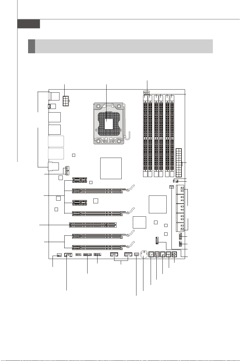
Quick Components Guide
Back Panel,
En-14
SYSFAN1/4,
En-17
PCIE slots,
En-23
PCI slot,
En-30
PCIE slots,
En-23
JPWR2, En-13
SYSFAN3,
En-17
J1394_1, En-17
CPU, En-5
JCOM1,
En-18
JTPM1, En-19
JUSB1/2,
En-20
CPUFAN1, En-17
D-LED2, En-21
GreenPower button, En-21
OC Dial button, En-22
OC Dial knob, En-22
SYSFAN5, En-17
DDR3, En-9
JPWR1, En-13
JCI1, En-19
JSMB1, En-20
SATA1~10,
En-16
JFP1, En-18
JFP2, En-18
SYSFAN2, En-17
JDLED2, En-19
POWER1, En-21
RESET1, En-21
En-4
Page 14
CPU (Central Processing Unit)
When you are installing the CPU, make sure to install the cooler to prevent
overheating. If you do not have the CPU cooler, consult your dealer before turning
on the computer.
For the latest information about CPU, please visit http://global.msi.com.tw/index.php?
func=cpuform2
Important
Overheating
Overheating will seriously damage the CPU and system. Always make sure
the cooling fan can work properly to protect the CPU from overheating. Make
sure that you apply an even layer of thermal paste (or thermal tape) between
the CPU and the heatsink to enhance heat dissipation.
Replaceing the CPU
While replacing the CPU, always turn off the ATX power supply or unplug the
power supply’s power cord from the grounded outlet first to ensure the safety
of CPU.
Overclocking
This mainboard is designed to support overclocking. However, please make
sure your components are able to tolerate such abnormal setting, while
doing overclocking. Any attempt to operate beyond product specifications is
not recommended. We do not guarantee the damages or risks caused
by inadequate operation or beyond product specifications.
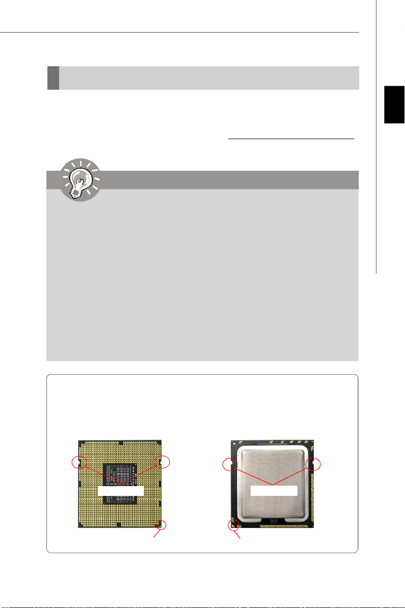
Introduction to LGA 1366 CPU
The pin-pad side of LGA 1366
CPU.
The surface of LGA 1366 CPU.
Remember to apply some thermal paste on it for better heat
dispersion.
English
Alignment Key
Yellow triangle is the Pin 1 indicator
Alignment Key
Yellow triangle is the Pin 1 indicator
En-5
Page 15
MS-7566 Mainboard
CPU & Cooler Installation
When you are installing the CPU, make sure the CPU has a cooler attached on
the top to prevent overheating. Meanwhile, do not forget to apply some thermal
paste on CPU before installing the heat sink/cooler fan for better heat dispersion.
Follow the steps below to install the CPU & cooler correctly. Wrong installation will
cause the damage of your CPU & mainboard.
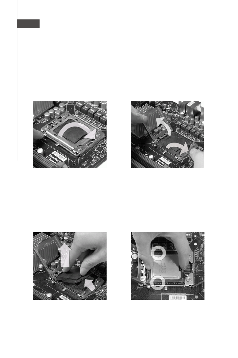
1. Open the load level.
2.Lift the load lever up and open the
load plate.
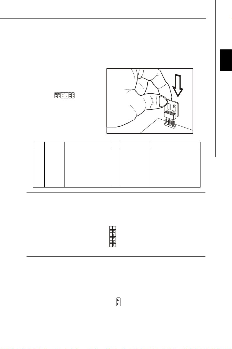
3. The CPU socket has a plastic cap on it
to protect the contack from damage.
Before you install CPU, always cover
it to protect the socket pin. Romove
the cap from the lever hinge side (as
the arrow shows).
En-6
4.After confirming the CPU direction for
correct mating, put down the CPU in
the socket housing frame. Be sure to
grasp on the edge of the CPU base.
Note that the alignment keys are
matched.
alignment key
Page 16
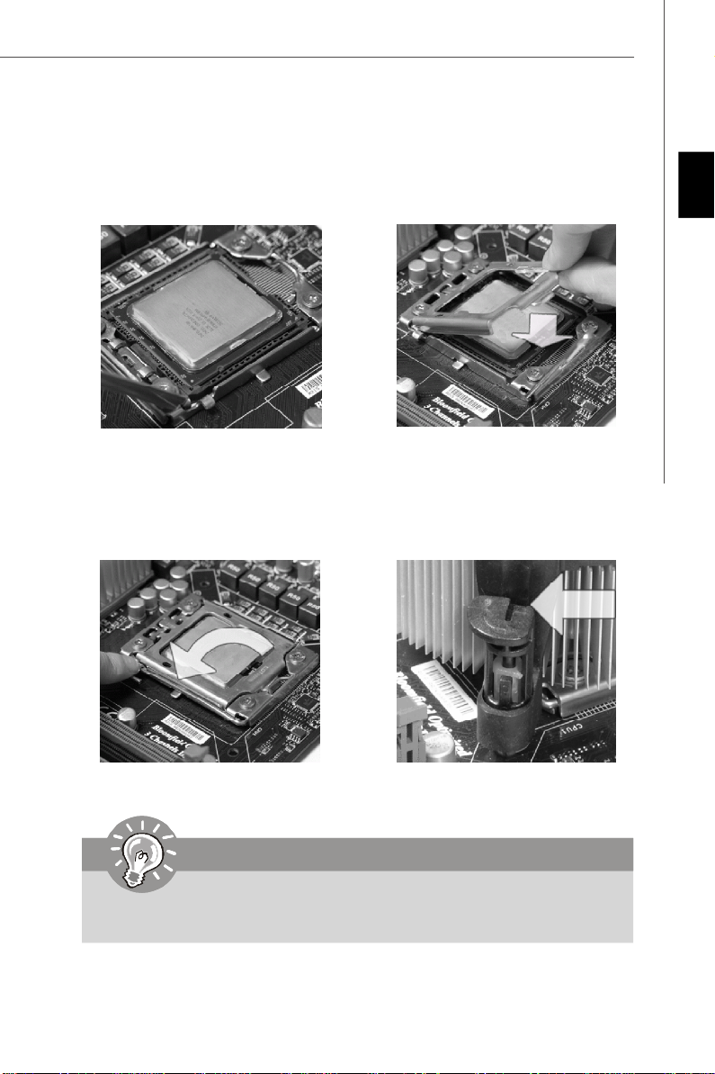
5.Visually inspect if the CPU is seated
well into the socket. If not, take out
the CPU with pure vertical motion and
reinstall.
6.Cover the load plate onto the
package.
English
7.Press down the load lever lightly onto
the load plate, and then secure the
lever with the hook under retention
tab.
8.Inspect the four hooks are in porper
position before you install the cooler.
Important
1.Confirm if your CPU cooler is firmly installed before turning on your system.
2. Do not touch the CPU socket pins to avoid damaging.
En-7
Page 17
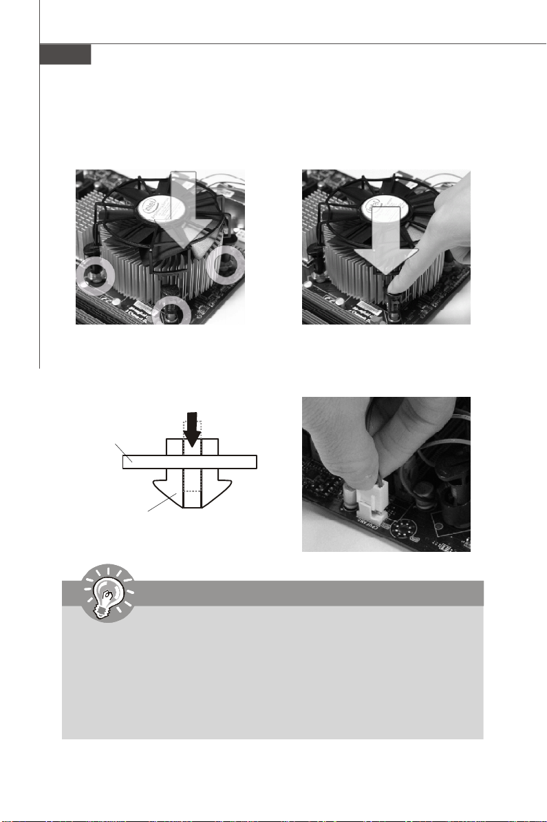
MS-7566 Mainboard
9.Align the holes on the mainboard with
the heatsink. Push down the cooler
until its four clips get wedged into
the holes of the mainboard.
11. Turn over the mainboard to confirm
that the clip-ends are correctly
inserted.
Mainboard
10.Press the four hooks down to fasten the cooler.
12. Finally, attach the CPU Fan cable to
the CPU fan connector on the
mainboard.
Hook
Important
1. Read the CPU status in BIOS.
2. Whenever CPU is not installed, always protect your CPU socket pin with the
plastic cap covered (shown in Figure 1) to avoid damaging.
3. Mainboard photos shown in this section are for demonstration of the CPU/
cooler installation only. The appearance of your mainboard may vary depending on the model you purchase.
4. Please refer to the documentation in the CPU fan package for more details
about the CPU fan installation.
En-8
Page 18
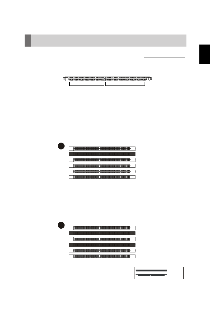
Memory
Installed
1
2
These DIMM slots are used for installing memory modules.
For more information on compatible components, please visit http://global.msi.com.
tw/index.php?func=testreport
DDR3
240-pin, 1.5V
48x2=96 pin
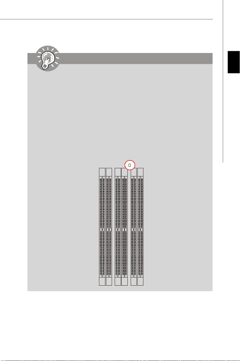
Memory Population Rules
Please refer to the following illustrations for memory population rules.
Single-Channel mode
When you have only one memory module, please always insert it into the DIMM_A0
first (as way 1 shown in below).
Dual-Channel mode
In Dual-Channel mode, the memory modules can transmit and receive data with two
data bus lines simultaneously. Enabling Dual-Channel mode can enhance the system
performance. When you have two memory modules, please always insert them into
the DIMM_A0 & DIMM_B0 (as way 2 shown in below).
72x2=144 pin
DIMM_A1
DIMM_A0
DIMM_B1
DIMM_B0
DIMM_C1
DIMM_C0
English
DIMM_A1
DIMM_A0
DIMM_B1
DIMM_B0
DIMM_C1
DIMM_C0
Empty
En-9
Page 19
MS-7566 Mainboard
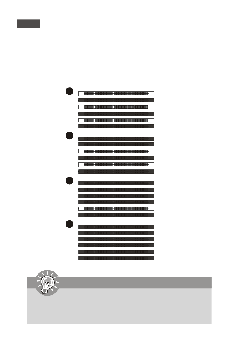
3
4
5
6
Triple-Channel mode
In Triple-Channel mode, the memory modules can transmit and receive data with
three data bus lines simultaneously. Enabling Triple-Channel mode can enhance the
best system performance. When you have three or more memory modules, please
always insert them as the way 3/ 4/ 5/ 6 (shown in below) to get the best system
performance.
DIMM_A1
DIMM_A0
DIMM_B1
DIMM_B0
DIMM_C1
DIMM_C0
DIMM_A1
DIMM_A0
DIMM_B1
DIMM_B0
DIMM_C1
DIMM_C0
DIMM_A1
DIMM_A0
DIMM_B1
DIMM_B0
DIMM_C1
DIMM_C0
DIMM_A1
DIMM_A0
DIMM_B1
DIMM_B0
DIMM_C1
DIMM_C0
-According to Intel CPU SPEC, DIMMs with voltage setting over 1.65V may
damage the CPU permanently. We recommend you install the DIMMs with the
voltage setting below 1.65V.
En-10
Page 20
Important
-DDR3 memory modules are not interchangeable with DDR2 and the DDR3
standard is not backwards compatible. You should always install DDR3
memory modules in the DDR3 DIMM slots.
-In Triple/ Dual-Channel mode, make sure that you install memory modules of
the same type and density in different channel DIMM slots.
-To enable successful system boot-up, always insert the memory modules
into the DIMM_A0 first.
- Due to the chipset resource deployment, the system density will only be
detected up to 23+GB (not full 24GB) when each DIMM is installed with a 4GB
memory module.
- When you install incorrect memory module (the SA2-pin of the memory
module connects to Ground) in the DIMM_C0/C1, the LED beside DIMM_C0
will light red color to remind you. The position of the LED is shown as below.
Double confirm with your memory module vender for the third channel supports.
English
En-11
Page 21
MS-7566 Mainboard
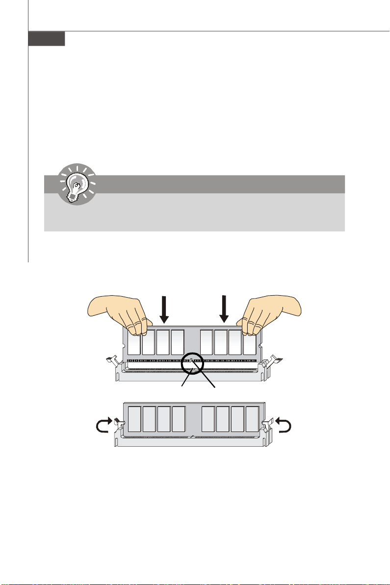
Installing Memory Modules
1. The memory module has only one notch on the center and will only fit in the right
orientation.
2. Insert the memory module vertically into the DIMM slot. Then push it in until the
golden finger on the memory module is deeply inserted in the DIMM slot. The plastic
clip at each side of the DIMM slot will automatically close when the memory module
is properly seated.
Important
You can barely see the golden finger if the memory module is properly inserted
in the DIMM slot.
3. Manually check if the memory module has been locked in place by the DIMM slot
clips at the sides.
En-12
Volt
Notch
Page 22
Power Supply
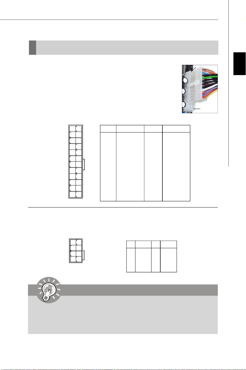
ATX 24-Pin Power Connector: JPWR1
This connector allows you to connect an ATX 24-pin power supply.
To connect the ATX 24-pin power supply, make sure the plug of the
power supply is inserted in the proper orientation and the pins are
aligned. Then push down the power supply firmly into the connector.
You may use the 20-pin ATX power supply as you like. If you’d like
to use the 20-pin ATX power supply, please plug your power supply along with pin 1 & pin 13 (refer to the image at the right hand).
Pin Definition
PIN SIGNAL
13 +3.3V
14 -12V
15 GND
16 PS-ON#
17 GND
18 GND
19 GND
20 Res
21 +5V
22 +5V
23 +5V
24 GND
JPWR1
12
1
24
13
PIN SIGNAL
1 +3.3V
2 +3.3V
3 GND
4 +5V
5 GND
6 +5V
7 GND
8 PWR OK
9 5VSB
10 +12V
11 +12V
12 +3.3V
ATX 8-Pin Power Connector: JPWR2
This power connector is used to provide power to the CPU.
Pin Definition
PINSIGNAL
1 GND
2 GND
3 GND
4 GND
PINSIGNAL
5 +12V
6 +12V
7 +12V
8 +12V
JPWR2
4
1
8
5
pin 13
pin 12
English
Important
1. Make sure that all the connectors are connected to proper ATX power supplies to ensure stable operation of the mainboard.
2. Power supply of 450 watts (and above) is highly recommended for system
stability.
3. ATX 12V power connection should be greater than 18A.
En-13
Page 23
MS-7566 Mainboard
Back Panel
Mouse
Keyboard
USB Ports
1394 Port (optional)
LAN
Clear CMOS
Button
eSATA Ports
USB Ports
Debug LED
Mouse/Keyboard
The standard PS/2® mouse/keyboard DIN connector is for a PS/2® mouse/keyboard.
Clear CMOS Button
There is a CMOS RAM on board that has a power supply from external battery to
keep the system configuration data. With the CMOS RAM, the system can automatically boot OS every time it is turned on. If you want to clear the system configuration,
use the button to clear data. Press the button to clear the data.
Important
Make sure that you power off the system before clearing CMOS data.
1394 Port (optional)
The IEEE1394 port on the back panel provides connection to IEEE1394 devices.
eSATA Port
The eSATA port is for attaching the eSATA external hard drive.
LAN
The standard RJ-45 LAN jack is for connection to
the Local Area Network (LAN). You can connect
a network cable to it.
LED Color LED State Condition
Off LAN link is not established.
Left Yellow On (steady state) LAN link is established.
On (brighter & pulsing)The computer is communicating with another computer on the LAN.
Green Off 10 Mbit/sec data rate is selected.
Right On 100 Mbit/sec data rate is selected.
Orange On 1000 Mbit/sec data rate is selected.
En-14
Green / OrangeYellow
Page 24
USB Port
The USB (Universal Serial Bus) port is for attaching USB devices such as keyboard,
mouse, or other USB-compatible devices.
Debug LED
Please refer to the table below to get more information about the Debug LED message.
Post Status
FF Power on and first initialize CPU.
C0, C1, C2 Early CPU Initialize.
C4, C6 Initialize chipset.
D4, D5 Initialize memory.
08 Initialize keyboard.
2A, 31 Initialize onboard devices. Load Option ROM (VGA and RAID
option ROM) form BIOS to memory.
37 Displaying sign-on message, CPU information, setup key
message and any OEM specific information.
38 Initialize USB device and different devices.
3C Mid POST initialization of chipset registers. Detect different
devices (parallel ports, serial ports and coprocessor in CPU…etc.)
75, 78 Initialize INT 13 devices and IPL devices. (include SATA/ PATA
HDD and CD/DVD ROM).
87 Enter setup screen. BIOS setup if needed/ requested.
A4 Wait for user input at configuration display if needed.
A7 Display the system configuration screen if enabled.
B1 Save system context for ACPI (Advanced Configuration and Power
Interface). Prepare give control to OS loader (INT 19H).
00 Pass control to OS Loader (typically INT 19H).
AA Enter OS (Vista or Windows XP).
English
En-15
Page 25
MS-7566 Mainboard
Connectors
Serial ATA Connector: SATA1~10
This connector is a high-speed Serial ATA interface port. Each connector can connect
to one Serial ATA device.
SATA1_3
SATA2_4
SATA5_6
SATA7_8
SATA9_10
SATA1~6
are supported by ICH10R
SATA7~8
are supported by first JMB322
SATA9~10
are supported by second JMB322
Important
1. Please do not fold the Serial ATA cable into 90-degree angle. Otherwise,
data loss may occur during transmission.
2. Please always use the Intel default SATA connectors (SATA1~6) first.
En-16
Page 26
Fan Power Connectors: CPUFAN1, SYSFAN1~5
The fan power connectors support system cooling fan with +12V. When connecting
the wire to the connectors, always note that the red wire is the positive and should
be connected to the +12V; the black wire is Ground and should be connected to GND.
If the mainboard has a System Hardware Monitor chipset on-board, you must use a
specially designed fan with speed sensor to take advantage of the CPU fan control.
+12V
SENSOR
CONTROL
GND
CPUFAN1
GND
+12V
SENSOR
GND
+12V
SENSOR
SYSFAN1 SYSFAN2
+12V
SENSOR
GND
SYSFAN3
GND
+12V
NC
+12V
NC
GND
SYSFAN4 SYSFAN5
Important
1.Please refer to the recommended CPU fans at processor’s official website
or consult the vendors for proper CPU cooling fan.
2.CPUFAN1 supports fan control. You can install Overclocking Center utility that will automatically control the CPU fan speed according to the actual
CPU temperature.
3. SYSFAN1~3 support fan control, too. You may select how percentage of
speed for the SYSFAN1/2/3 in BIOS.
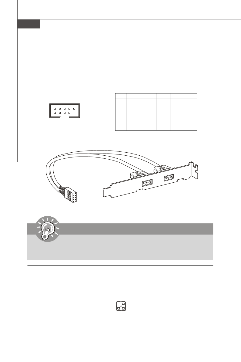
IEEE1394 Connector: J1394_1 (optional)
This connector allows you to connect the IEEE1394 device via an optional IEEE1394
bracket.
Pin Definition
PIN SIGNAL PIN SIGNAL
9
10
J1394_1
1
2
1 TPA+ 2 TPA3 Ground 4 Ground
5 TPB+ 6 TPB7 Cable power 8 Cable power
9 Key (no pin) 10 Ground
English
IEEE1394 Bracket (Optional)
En-17
Page 27
MS-7566 Mainboard
Front Panel Connectors: JFP1, JFP2
These connectors are for electrical connection to the front panel switches and LEDs.
The JFP1 is compliant with Intel® Front Panel I/O Connectivity Design Guide.
JFP1 Pin Definition
PIN SIGNAL DESCRIPTION
1 HD_LED + Hard disk LED +
2 PWR/SLP LED MSG LED
3 HD_LED - Hard disk LED 4 PWR/SLP LED MSG LED
5 RST_SW - Reset Switch 6 PWR_SW + Power Switch +
7 RST_SW + Reset Switch +
8 PWR_SW - Power Switch 9 RSVD Reserved. Do not use.
JFP2 Pin Definition
PIN SIGNAL DESCRIPTION
7
Power
LED
12
1 GND Ground
2 SPK- Speaker3 SLED Suspend LED
4 BUZ+ Buzzer+
5 PLED Power LED
6 BUZ- Buzzer7 NC Key (No Pin)
8 SPK+ Speaker+
Power
Switch
Power
LED
JFP1
10
+
2
Speaker
1
9
+
Reset
-
Switch
-
HDD
+
LED
8
+
+
-
JFP2
Serial Port Connector: JCOM1
This connector is a 16550A high speed communication port that sends/receives 16
bytes FIFOs. You can attach a serial device.
Pin Definition
PIN SIGNAL DESCRIPTION
1 DCD Data Carry Detect
2 SIN Serial In or Receive Data
3 SOUT Serial Out or Transmit Data
4 DTR Data Terminal Ready
5 GND Ground
6 DSR Data Set Ready
7 RTS Request To Send
8 CTS Clear To Send
9 RI Ring Indicate
En-18
JCOM1
2
1 9
10
Page 28
TPM Module Connector: JTPM1
This connector connects to a TPM (Trusted Platform Module) module (optional). Please
refer to the TPM security platform manual for more details and usages.
English
2
1
14
13
JTPM1
Pin Signal Description Pin Signal Description
1 LCLK LPC clock 2 3V_STB 3V standby power
3 LRST# LPC reset 4 VCC3 3.3V power
5 LAD0 LPC address & data pin0 6 SIRQ Serial IRQ
7 LAD1 LPC address & data pin1 8 VCC5 5V power
9 LAD2 LPC address & data pin2 10 KEY No pin
11 LAD3 LPC address & data pin3 12 GND Ground
13 LFRAME# LPC Frame 14 GND Ground
D-LED2 Connector: JDLED2
This connector connects to a D-LED2 (Debug-LED2) panel (optional), which shows
information on the panel for you and identify the current status or mode of the
connected system. Please refer to the D-LED2 quick guide for more details and
usages.
JDLED2
1112
12
Chassis Intrusion Connector: JCI1
This connector connects to the chassis intrusion switch cable. If the chassis is
opened, the chassis intrusion mechanism will be activated. The system will record
this status and show a warning message on the screen. To clear the warning, you
must enter the BIOS utility and clear the record.
CINTRU
GND
1
2
JCI1
En-19
Page 29
MS-7566 Mainboard
Front USB Connector: JUSB1/ JUSB2
These connectors, compliant with Intel® I/O Connectivity Design Guide, is ideal for
connecting high-speed USB interface peripherals such as USB HDD, digital cameras,
MP3 players, printers, modems and the like.
Pin Definition
JUSB1/ JUSB2
2
1
10
9
PIN SIGNAL PIN SIGNAL
1 VCC 2 VCC
3 USBD- 4 USBD5 USBD+ 6 USBD+
7 GND 8 GND
9 Key (no pin) 10 NC
USB 2.0 Bracket
(optional)
Important
Note that the pins of VCC and GND must be connected correctly to avoid
possible damage.
GreenPower Genie Connector: JSMB1
This connector connects to GreenPower Genie (optional). Please refer to the
GreenPower Genie manual for more details and usages.
1
2
JSMB1
En-20
Page 30
Buttons and Knob
The motherboard provides the following buttons for you to set the computer’s function.
This section will explain how to change your motherboard’s function through the use
of button.
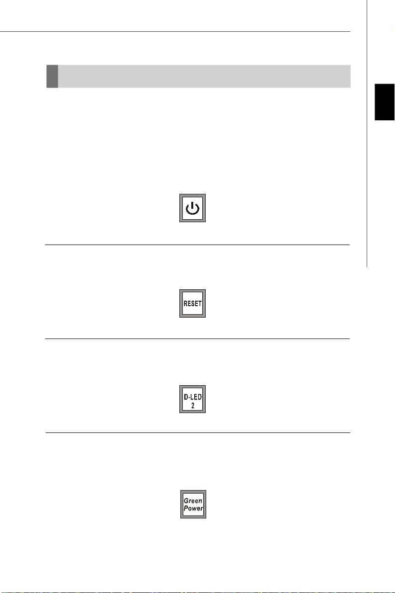
Power Button: POWER1
This power button is used to turn-on or turn-off the system. Press the button to turnon or turn-off the system. This button will light after you power-on the system, and
the light will turn-off when you power-off the system.
POWER1
Reset Button: RESET1
This reset button is used to reset the system. Press the button to reset the system.
This button will light when the system is in S0 status.
RESET1
D-LED2 Button: DLED2
This button is used to change the menu on D-LED2 panel. Press the button to change
the menu on D-LED2 panel. Please refer to the D-LED2 quick guide for more details
and usages.
English
DLED2
GreenPower Button
This button is used to switch GreenPower function of system. Once you press the
button, the system will switch the GreenPower between disable and auto mode.
En-21
Page 31

MS-7566 Mainboard
OC Dial Button and OC Dial Knob
These button and knob are used to adjust the FSB.
OC Dial Knob OC Dial Button
You can use them to change base clock at any time under the operating systems.
This method does not need to install software or reboot. Please follow the steps
below to increase or decrease the frequency of base clock.
1.Press the OC Dial button to start adjustment. The OC Dial LED will light to indicate
current operation.
2.Turn the OC Dial knob clockwise/anti-clockwise to increase/decrease base clock.
You can set the value of OC Dial Step in BIOS.
3.Press the OC Dial button again to complete adjustment. The OC Dial LED will turn off
automatically.
Important
1.In order to increase the success rate, you should set parameters of voltage
in BIOS properly, before you use OC Dial function to overclock the system.
2.After each of the adjustments, this feature should be shut down. Otherwise,
it would affect the system performance. Therefore, when you complete the
adjustment, check whether OC Dial LED is on or off, if OC Dial LED is still
lit, press the button and then check again.
En-22
Page 32

Slots
PCI (Peripheral Component Interconnect) Express Slot
The PCI Express slot supports the PCI Express interface expansion card.
The PCI Express 2.0 x16 supports up to 8.0 GB/s transfer rate.
The PCI Express 2.0 x4 supports up to 2.0 GB/s transfer rate.
The PCI Express 1.0 x1 supports up to 250 MB/s transfer rate.
PCI_E1 supports up to PCI Express 1.0 x1 speed
PCI_E2 supports up to PCI Express 2.0 x16 speed
PCI_E3 supports up to PCI Express 1.0 x1 speed
PCI_E4 supports up to PCI Express 2.0 x16 speed
PCI_E5 supports up to PCI Express 2.0 x16 speed
English
PCI_E6 supports up to PCI Express 2.0 x4 speed
Important
1.The mainboard supports ATI CrossFireXTM technology and NVIDIA SLI
Multi Graphic solution.
2When adding or removing expansion cards, make sure that you unplug the
power supply first. Meanwhile, read the documentation for the expansion
card to configure any necessary hardware or software settings for the expansion card, such as jumpers, switches or BIOS configuration.
En-23
TM
Page 33

MS-7566 Mainboard
ATI CrossFireXTM (Multi-GPU) Technology
ATI CrossFireXTM is the ultimate multi-GPU performance gaming platform. Enabling
game-dominating power, ATI CrossFireXTM technology enables two or more discrete
graphics processors to work together to improve system performance. ATI CrossFireX
technology allows you to expand your system’s graphics capabilities. It allows you
the ability to scale your system’s graphics horsepower as you need it, supporting up
to two or more ATI RadeonTM HD graphics cards, making this the most scalable gaming
platform ever. The mainboard can auto detect the CrossFireXTM mode by software,
therefore you don’t have to enable the CrossFireXTM in BIOS by yourself. The following details the 2-way CrossFireXTM installation.
1. Install one ATI RadeonTM HD graphics card in the first PCIE x16 (PCI_E2) slot , then
install one ATI RadeonTM HD graphics card in the second PCIE x16 (PCI_E4) slot.
2. With two cards installed, an CrossFireXTM Video Link cable is required to connect
the golden fingers on the top of these two graphics cards (refer to the picture
below). Please note that although you have installed two or more graphics cards,
only the video outputs on the graphics card installed in PCI_E2 will work. Hence,
you only need to connect a monitor to this graphics card.
CrossFireXTM Video Link cable
Important
1. Mainboard photos shown in this section are for demonstration only. The
appearance of your mainboard may vary depending on the model you purchase.
2. If you intend to install TWO graphics cards for CrossFireXTM mode, make
sure that:
a. these graphics cards are of the same brand and specifications;
b. these graphics cards are installed on PCIE_E2 & PCI_E4 slots.
3. Make sure that you connect an adequate power supply to the power connector on the graphics card to ensure stable operation of the graphics card.
4. Only Windows® XP with Service Pack 2 (SP2)& Windows® XP Profes
-sional x64 Edition & Windows® Vista support the CrossFireXTM function.
En-24
Page 34

3.When all of the hardware and software has been properly set up and installed,
reboot the system. After entering the O.S., click the “Catalyst ™ Control Center”
icon on the desktop. There is a setting in the Catalyst™ Control Center that
needs to be enabled for CrossFireX™ to operate. The following aspect appears in
Catalyst™ Control Center:
Select the
Advanced View
from the view
drop menu.
English
Important
A CrossFireX™ system has four possible display modes:
• SuperTiling
• Scissor Mode
• Alternate Frame Rendering
• Super Anti-aliasing.
for more details, please consult the graphics card manual from the
manufacturer.
En-25
Page 35

MS-7566 Mainboard
NVIDIA 3-Way SLI Technology
NVIDIA 3-Way SLI (Scalable Link Interface) technology allows three GPUs to run in
sequence within a system to achieve up to triple the performance of a single graphics card. To utilize this technology, the three GPU cards must be connected by 3-Way
SLI bridge cables. Please refer to the following illustrations for enabling the 3-Way
SLI technology.
3-Way SLI bridge
short cable
3-Way SLI bridge
long cable
Important
Before you configure the 3-SLI platform hardware, please make sure that:
1. The three graphics cards have to support 3-Way SLI technology and they
are of the same brand and specifications;
2. The 3-Way SLI platform requires specific power supply requirement
which provide the minimum 1000W peak power to support the needs of
three graphics cards in the system;
3. The 3-Way SLI platform also requires a chassis that meet the qualifictions
for running 3-way NVIDIA SLI.
4. To visit the NVIDIA official website and find the GPUs, power supply and
chassis that should be approved for 3-Way SLI.
En-26
Page 36

1.Installing three graphics cards which support 3-Way SLI technology on black PCI
Express x16 slots. After three cards installed, SLI Bridge cables are required to
connect the golden fingers on the top of these three graphics cards (fig.1). Please
note that although you have installed three graphics cards, only the video outputs
on the first card (which be installed in PCI_E2 slot) will work. Hence, you only need
to connect a monitor to the first PCI Express card.
English
Fig.1 3-Way SLI Bridge cables connection
En-27
Page 37

MS-7566 Mainboard
Important
1.Mainboard photos shown in this section are for demonstration only. The
appearance of your mainboard may vary depending on the model you purchase.
2.If you intend to install only ONE x16 graphics card, please install this
graphics card in first PCIE x16 (PCI_E2) slot to run full x16 speed.
3.If you wish to use 2-way SLI, you must install the two graphics cards in first
and second PCIE x16 slots (PCI_E2 & PCI_E4). Then, connect two graphics cards together using the 2 SLI bridge short cables (Fig.2). And remember to enable the SLI technology function as the following step 2 & step 3.
4.3-Way SLI technology supports Windows® Vista only.
En-28
Fig.2 2-Way SLI Bridge cables connection
Page 38

2.After the hardware installation is completed, power on the system and install the
NVIDIA ForceWare Windows Vista driver. Reboot the system, a NVIDIA Control
Panel will be provided for Multi-GPU control. Right click on windows desktop and
select NVIDIA Control Panel. Go to 3D Settings --> Set SLI configuration and
check Enable SLI technology (recommended). Then press Apply. (concerning
the details of multi-GPU settings, please refer to your graphics card manual).
Check the box
3.Go to 3D Settings on the top menu options, and check the Show SLI Visual
Indicators. It will show the SLI x3 lable and a scaling bar in fullscreen 3D
applications.
English
Important
If you want to quit the SLI function, make sure that you disable the "SLI
technology" function.
En-29
Page 39

MS-7566 Mainboard
PCI (Peripheral Component Interconnect) Slot
The PCI slot supports LAN card, SCSI card, USB card, and other add-on cards that
comply with PCI specifications.
Important
This PCI slot doesn’t support 64bit PCI cards.
PCI Interrupt Request Routing
The IRQ, acronym of interrupt request line and pronounced I-R-Q, are hardware lines
over which devices can send interrupt signals to the microprocessor. The PCI IRQ
pins are typically connected to the PCI bus pins as follows:
Order 1 Order 2 Order 3 Order 4
PCI Slot 1 INT A# INT B# INT C# INT D#
En-30
Page 40

LED Status Indicators
ICH10R SATA LED
JMB322 RAID LED
OC Dial LED
HDD LED
Suspend LED
Power LED
DDR Phase LEDs
CPU Load Line LED
DLED
English
CPU Phase LEDs
QPI Phase LEDs
eSATA LED
IOH Phase LEDs
PCIE LEDs
PCI LED
DIMM Warning LED
CPU Phase LEDs
These LEDs indicate the current CPU power phase mode. Follow the instructions
below to read.
6 of the LEDs will light blue when CPU is in 6 phase power mode.
5 of the LEDs will light blue when CPU is in 5 phase power mode.
4 of the LEDs will light blue when CPU is in 4 phase power mode.
3 of the LEDs will light blue when CPU is in 3 phase power mode.
2 of the LEDs will light blue when CPU is in 2 phase power mode.
1 of the LEDs will light blue when CPU is in 1 phase power mode.
QPI Phase LEDs
These LEDs indicate the current QPI power phase mode. Follow the instructions
below to read.
2 of the LEDs will light blue when QPI is in 2 phase power mode.
1 of the LEDs will light blue when QPI is in 1 phase power mode.
En-31
Page 41

MS-7566 Mainboard
CPU Load Line LED
Lights blue when the CPU load line is optimized.
IOH Phase LEDs
These LEDs indicate the current IOH power phase mode. Follow the instructions
below to read.
2 of the LEDs will light blue when IOH is in 2 phase power mode.
1 of the LEDs will light blue when IOH is in 1 phase power mode.
DDR Phase LEDs
These LEDs indicate the current memory power phase mode. Follow the instructions
below to read.
3 of the LEDs will light blue when memory is in 3 phase power mode.
2 of the LEDs will light blue when memory is in 2 phase power mode.
1 of the LEDs will light blue when memory is in 1 phase power mode.
DIMM Warning LED
Lights red when the incorrect memory installed into DIMM_C0/ DIMM_C1 (the DIMMs
of 3rd channel).
Power LED
Lights green when the system is in power-on(S0/S1) status.
Suspend LED
Lights yellow when the system is suspended (S3/S4/S5 ).
HDD LED
Lights red when hard disk drives are reading or writing.
PCIE and PCI LEDs
Lights blue when the slots is functional.
En-32
Page 42

eSATA LED
Lights red when the eSATA hard disk drives are reading or writing.
ICH10R SATA LED
Lights red when hard disk drives which connected to ICH10R are reading or writing.
JMB322 RAID LED
Lights blue when the RAID hard disk drives are reading or writing.
OC Dial LED
Lights blue when the OC Dial is operating.
English
En-33
Page 43

MS-7566 Mainboard
BIOS Setup
This chapter provides basic information on the BIOS Setup program and allows you to
configure the system for optimum use. You may need to run the Setup program
when:
* An error message appears on the screen during the system booting up, and requests you to run BIOS SETUP.
* You want to change the default settings for customized features.
Important
1.The items under each BIOS category described in this chapter are under
continuous update for better system performance. Therefore, the description
may be slightly different from the latest BIOS and should be held for reference
only.
2.Upon boot-up, the 1st line appearing after the memory count is the BIOS
version. It is usually in the format:
1st digit refers to BIOS maker as A = AMI, W = AWARD, and P = PHOENIX.
2nd - 5th digit refers to the model number.
6th refers to the Chipset vender as A = AMD, I = Intel, V = VIA, N = Nvidia, U =
ULi.
7th - 8th digit refers to the customer as MS = all standard customers.
V1.0 refers to the BIOS version.
010109 refers to the date this BIOS was released.
A7566IMS V1.0 010109 where:
En-34
Page 44

Entering Setup
Power on the computer and the system will start POST (Power On Self Test) process.
When the message below appears on the screen, press <DEL> key to enter Setup.
Press DEL to enter SETUP
If the message disappears before you respond and you still wish to enter Setup,
restart the system by turning it OFF and On or pressing the RESET button. You may
also restart the system by simultaneously pressing <Ctrl>, <Alt>, and <Delete> keys.
Getting Help
After entering the Setup menu, the first menu you will see is the Main Menu.
Main Menu
The main menu lists the setup functions you can make changes to. You can use the
arrow keys (↑↓ ) to select the item. The on-line description of the highlighted setup
function is displayed at the bottom of the screen.
Sub-Menu
If you find a right pointer symbol (as shown in the right view)
appears to the left of certain fields that means a sub-menu
containing additional options can be launched from this field.
You can use control keys (↑↓ ) to highlight the field and
press <Enter> to call up the sub-menu. Then you can use the control keys to enter
values and move from field to field within a sub-menu. If you want to return to the
main menu, just press <Esc >.
General Help <F1>
The BIOS setup program provides a General Help screen. You can call up this screen
from any menu by simply pressing <F1>. The Help screen lists the appropriate keys
to use and the possible selections for the highlighted item. Press <Esc> to exit the
Help screen.
English
En-35
Page 45

MS-7566 Mainboard
The Main Menu
Once you enter AMI® or AWARD® BIOS CMOS Setup Utility, the Main Menu will appear
on the screen. The Main Menu allows you to select from functions and exit choices.
Use arrow keys to select among the items and press <Enter> to accept or enter the
sub-menu.
Standard CMOS Features
Use this menu for basic system configurations, such as time, date etc.
Advanced BIOS Features
Use this menu to setup the items of AMI® special enhanced features.
Integrated Peripherals
Use this menu to specify your settings for integrated peripherals.
Power Management Setup
Use this menu to specify your settings for power management.
H/W Monitor
This entry shows your PC health status.
Green Power
Use this menu to specify the power phase.
BIOS Setting Password
Use this menu to set the password for BIOS.
Cell Menu
Use this menu to specify your settings for frequency/voltage control and overclocking.
User Settings
Use this menu to save/ load your settings to/ from CMOS for BIOS.
M-Flash
Use this menu to read/ flash the BIOS from storage drive (FAT/ FAT32 format only).
Load Fail-Safe Defaults
Use this menu to load the default values set by the BIOS vendor for stable system
performance.
Load Optimized Defaults
Use this menu to load the default values set by the mainboard manufacturer specifically for optimal performance of the mainboard.
Save & Exit Setup
Save changes to CMOS and exit setup.
Exit Without Saving
Abandon all changes and exit setup.
En-36
Page 46

When enter the BIOS Setup utility, follow the processes below for general use.
1. Load Optimized Defaults : Use control keys (↑↓) to highlight the Load Opti-
mized Defaults field and press <Enter> , a message as below appears:
Select [Ok] and press Enter to load the default settings for optimal system
performance.
2. Setup Date/ Time : Select the Standard CMOS Features and press <Enter> to
enter the Standard CMOS Features-menu. Adjust the Date, Time fields.
3. Save & Exit Setup : Use control keys (↑↓) to highlight the Save & Exit Setup
field and press <Enter> , a message as below appears:
English
Select [Ok] and press Enter to save the configurations and exit BIOS Setup utility.
Important
The configuration above are for general use only. If you need the detailed
settings of BIOS, please see the manual in English version on MSI website.
En-37
Page 47

MS-7566 Mainboard
4. Cell Menu Introduction : This menu is for advanced user who want to overclock
the mainboard.
Important
Change these settings only if you are familiar with the chipset.
Current Core / DRAM / QPI Frequency
These items show the current clocks of CPU and Memory speed. Read-only.
En-38
Page 48

CPU Specifications
Press <Enter> to enter the sub-menu and the following screen appears.
This sub-menu displays the informations of installed CPU.
CPU Technology Support
Press <Enter> to enter the sub-menu and the following screen appears.
English
This sub-menu displays the technologies that the installed CPU supported.
Intel EIST
The Enhanced Intel SpeedStep technology allows you to set the performance level of
the microprocessor whether the computer is running on battery or AC power. This
field will appear after you installed the CPU which support speedstep technology.
Intel C-STATE tech
C-state is a power management state that significantly reduces the power of the
processor during idle. This field will appear after you installed the CPU which support
c-state technology.
Base Clock (MHz)
This item allows you to set the CPU Base clock (in MHz).
En-39
Page 49

MS-7566 Mainboard
Intel Turbo Boost tech
This item will appear when you install a CPU include Intel Turbo Boost technology.
This item is used to enable/ disable Intel Turbo Boost technology. For further information please refer to Intel's official website.
Turbo Boost Tech Config
This sub-menu will appear when you install a CPU include Intel Turbo Boost technology.
Press <Enter> to enter the sub-menu and the following screen appears.
Turbo Ratio Limit Program
This item is used to enable/ disable the turbo ratio limit program. Setting to [Enabled]
activates the following fields, and use the following fields to set each CPU core
ratio.
#-Core Ratio Limit
These items allow you to select the CPU core ratio.
TDC Limit Override
Setting to [Enabled] activates the TDC Limit value field, and use the TDC Limit
value field to set the CPU TDC value.
TDC Limit value (A)
This item allows you to select the CPU TDC value (ampere).
TDP Limit Override
Setting to [Enable] activates the TDP Limit value field, and use the TDP Limit
value field to set the CPU TDP value.
TDP Limit value (W)
This item allows you to select the CPU TDP value (watt).
OC Dial Function
This item allows you to enable/disable the OC Dial function. Setting to [Enabled]
activates the following fields, and use the following fields to set each OC Dial function.
En-40
Page 50

OC Dial Step
This item is used to set value of each step when you rotate the OC dial knob.
OC Dial Reset
Select [Reset] if you need to reset the OC Dial Value.
OC Dial Value
This item indicates the overclocking value by OC dial function. When you rotate the
OC dial knob, this value will change.
OC Dial Adjusted Base Clock (MHz)
It shows the adjusted base clock by OC Dial function (Base Clock +OC Dial Value).
Read-only.
Adjusted Core Frequency (MHz)
It shows the adjusted CPU frequency (Base clock x Ratio). Read-only.
QPI Configuration
Press <Enter> to enter the sub-menu and the following screen appears.
QPI Links Speed
This item allows you to select the QPI links speed type.
QPI Frequency
This item allows you to select the QPI frequency.
Memory-Z
Press <Enter> to enter the sub-menu and the following screen appears.
English
En-41
Page 51

MS-7566 Mainboard
DIMM_A0,A1,B0,B1,C0,C1 Memory SPD Information
Press <Enter> to enter the sub-menu and the following screen appears.
This sub-menu displays the informations of installed memory.
X.M.P SUPPORT Information
Press <Enter> to enter the sub-menu and the following screen appears. These
items display the current status of the X.M.P support information such as ,
memory voltage, max bandwidth, SDRAM cycle time, DRAM TCL, DRAM TRCD,
DRAM TRP, DRAM TRAS, DRAM TRFC, DRAM TWR, DRAM TWTR, DRAM TRRD
and DRAM TRTP. They are read only.
Advance DRAM Configuration
Press <Enter> to enter the sub-menu and the following screen appears.
En-42
Page 52

1N/2N Memory Timing
This item controls the SDRAM command rate. Select [1N] makes SDRAM signal
controller to run at 1N (N=clock cycles) rate. Selecting [2N] makes SDRAM signal
controller run at 2N rate.
CAS# Latency (CL)
This controls the CAS latency, which determines the timing delay (in clock cycles)
before SDRAM starts a read command after receiving it.
tRCD
When DRAM is refreshed, both rows and columns are addressed separately.
This setup item allows you to determine the timing of the transition from RAS
(row address strobe) to CAS (column address strobe). The less the clock
cycles, the faster the DRAM performance.
tRP
This setting controls the number of cycles for Row Address Strobe (RAS) to be
allowed to precharge. If insufficient time is allowed for the RAS to accumulate its
charge before DRAM refresh, refresh may be incomplete and DRAM may fail to
retain data. This item applies only when synchronous DRAM is installed in the
system.
tRAS
This setting determines the time RAS takes to read from and write to memory
cell.
Advanced Memory Setting
Setting to [Auto] enables the advance memory timing automatically to be determined by BIOS. Setting to [Manual] allows you to set advanced memory timings.
Extreme Memory Profile
This item is used to enable/disable the Intel Extreme Memory Profile (XMP). For further
information please refer to Intel's official website.
English
Memory Ratio
This item allows you to set the memory multiplier.
Adjusted DRAM Frequency (MHz)
It shows the adjusted DDR Memory frequency. Read-only.
ClockGen Tuner
Press <Enter> to enter the sub-menu and the following screen appears.
En-43
Page 53

MS-7566 Mainboard
CPU / PCI Express Amplitude Control
These items are used to select the CPU/ PCI Express clock amplitude.
CPU CLK Skew/ IOH CLK Skew
These items are used to select the CPU/ IOH chipset clock skew. They can help
CPU to reach the higher overclocking performace.
Adjust PCI Frequency (MHz)
This field allows you to select the PCI frequency (in MHz).
Adjust PCI-E Frequency (MHz)
This field allows you to select the PCIE frequency (in MHz).
Auto Disable DRAM/PCI Frequency
When set to [Enabled], the system will remove (turn off) clocks from empty DIMM and
PCI slots to minimize the electromagnetic interference (EMI).
CPU Load Line Calibration
This item allows you to enable/disable CPU Load Line Calibration.
CPU Voltage (V)/ CPU Vcore/ QPI Voltage (V))/ CPU PLL Voltage (V)/ DRAM
Voltage (V)/ DDR_VREF_CA_A (V)/ DDR_VREF_CA_B (V)/ DDR_VREF_CA_C (V)/
DDR_VREF_DQ_A (V)/DDR_VREF_DQ_B (V), DDR_VREF_DQ_C (V)/ IOH Voltage
(V)/ IOH PCIE Voltage (V)/ ICH Voltage (V)/ nForce 200 Voltage (V)
These items are used to asjust the voltage of CPU, Memory, QPI and chipset.
For CPU Voltage:
The value here is the offset for you to adjust/add based on the current CPU voltage.
Please read the real-time CPU voltage in “CPU Vcore”. Please note the based CPU
Voltage will vary depending on the different CPU you install.
For QPI Voltage:
The value here is the offset for you to adjust/add based on the current QPI voltage.
The default based QPI Voltage is from 1.1V to 1.22V, and it will vary depending on the
different CPU you install. You can read the QPI voltage in GreenPower Center.
For DRAM Voltage:
According to the Inte CPU spec, DRAM Voltage setting 1.65V may damage the CPU
permanently. It is strongly recommended that you install the DRAM with the voltage
setting below 1.65V. You can read the DRAM voltage in GreenPower Center.
Spread Spectrum
When the motherboard’s clock generator pulses, the extreme values (spikes) of the
pulses create EMI (Electromagnetic Interference). The Spread Spectrum function
reduces the EMI generated by modulating the pulses so that the spikes of the pulses
are reduced to flatter curves. If you do not have any EMI problem, leave the setting at
Disabled for optimal system stability and performance. But if you are plagued by EMI,
set to Enabled for EMI reduction. Remember to disable Spread Spectrum if you are
overclocking because even a slight jitter can introduce a temporary boost in clock
speed which may just cause your overclocked processor to lock up.
En-44
Page 54

Important
1.If you do not have any EMI problem, leave the setting at [Disabled] for
optimal system stability and performance. But if you are plagued by EMI,
select the value of Spread Spectrum for EMI reduction.
2.The greater the Spread Spectrum value is, the greater the EMI is reduced,
and the system will become less stable. For the most suitable Spread
Spectrum value, please consult your local EMI regulation.
3.Remember to disable Spread Spectrum if you are overclocking because
even a slight jitter can introduce a temporary boost in clock speed which
may just cause your overclocked processor to lock up.
English
En-45
Page 55

MS-7566 Mainboard
Software Information
Take out the Driver/Utility DVD that is included in the mainboard package, and place it
into the DVD-ROM drive. The installation will auto-run, simply click the driver or utility
and follow the pop-up screen to complete the installation. The Driver/Utility DVD contains the:
Driver menu - The Driver menu shows the available drivers. Install the driver by your
desire and to activate the device.
Utility menu - The Utility menu shows the software applications that the mainboard
supports.
Service base menu - The Service base menu shows the necessary websites.
Important
Please visit the MSI website to get the latest drivers and BIOS for better
system performance.
En-46
Page 56

Eclipse Plus
Serie
Benutzerhandbuch
Deutsch
Deutsch
De-1
Page 57

MS-7566 Mainboard
Spezifikationen
Prozessoren
- Intel® Core i7 Prozessoren für Sockel LGA1366
(Weitere CPU Informationen finden Sie unter
http://global.msi.com.tw/index.php?func=cpuform2)
QPI
- Bis zu 25.6 GB/s
Chipsatz
- North-Bridge: Intel® X58 Chipsatz
- South-Bridge: Intel® ICH10R Chipsatz
Speicher
- 6 DDR3 DIMMs unterstützen DDR3 1600(OC)/ 1333/ 1066/ 800
SDRAM (max. 24GB)
- Unterstützt 3-Kanal
(Weitere Informationen zu kompatiblen Speichermodulen finden
Sie unter http://global.msi.com.tw/index.php?func=testreport)
LAN
- Unterstützt 2 PCIE LAN 10/100/1000 Fast Ethernet über Realtek
8111C
Audio (optional)
- Sound Blaster® X-Fi™ Xtreme Audio Karte
- 24-Bit / 96KHz Audio Qualität
- 100dB SNR Clarity
- Bis zu 7.1-Kanal EAX® 5.0 Surround Sound
SATA
- 6 SATAII Ports über Intel® ICH10R
- 4 SATAII Ports über JMicron® JMB322
- 2 E-SATA Ports über JMicron® JMB362
- Unterstützt Datenübertragungsraten von bis zu 3 Gb/s
RAID
- SATA1~6 unterstützen die Intel® Martix Storage Technologie (AHCI
+ RAID 0/1/5/10) über Intel® ICH10R
- SATA7/8 unterstützen die Modi RAID 0/ 1 (Hardware RAID) über 1st
JMicron® JMB322
- SATA9/10 unterstützen die Modi RAID 0/ 1 (Hardware RAID) über
2nd JMicron® JMB322
- Zwei E-SATA Ports auf hinteres Anschlusspanel unterstützen die
Modi RAID 0/ 1 & JBOD über JMicron JMB362
IEEE1394 (optional)
- 2 IEEE1394 Ports (Rückseite*1, onBoard*1) über VIA® VT6308
NVIDIA® nForce® 200
- Unterstützt NVIDIA® SLI™ Multi Grafik Auflösung
®
De-2
Page 58

ATI CrossFireX™
- Unterstützt ATI CrossFireX™
Anschlüsse
Hintere Ein-/ und Ausgänge
- 1 PS/2 Mausanschluss
- 1 PS/2 Tastaturanschluss
- 1 1394 Anschluss
- 2 eSATA Anschlüsse
- 8 USB 2.0 Anschlüsse
- 2 LAN Anschlüsse
- 1 Debug LED
- 1 CMOS leeren-Taste
On-Board Stiftleisten/ Anschlüsse
- 2 USB 2.0 Stiftleisten
- 1 1394 Stiftleiste (optional)
- 1 Gehäusekontaktschalter
- 1 Serielle Stiftleiste
- 1 TPM Module Stiftleiste
- 1 D-LED2 Stiftleiste
- 1 GreenPower Genie Anschluss
- 1 Ein-/ Aus-Schalter
- 1 Reset-Taste
- 1 D-LED2 Taste
- 1 GreenPower Taste
- 1 OC Dial Taste
- 1 OC Dial Knopf
TPM
- Unterstützt TPM
Steckplätze
- 3 PCI Express® gen2 x16 -Steckplätze
- 1 PCI Express® x16 -Steckplatz, unterstützt die Geschwindigkeit bis zu
PCI Express® Gen.2 x4
- 2 PCI Express® Gen.1 x1 -Steckplätze
- 1 PCI -Steckplätze, unterstützen 3.3V/ 5V PCI Bus Interface
Form Faktor
- ATX (30.5cm X 24.5cm)
Montage
- 9 Montagebohrungen
Deutsch
De-3
Page 59

MS-7566 Mainboard
DLED
Komponenten-Übersicht
Back Panel,
De-14
SYSFAN1/4,
De-17
PCIE slots,
De-23
PCI slot,
De-30
PCIE slots,
De-23
JPWR2, De-13
SYSFAN3,
De-17
J1394_1, De-17
CPU, De-5
JCOM1,
De-18
JTPM1, De-19
JUSB1/2,
De-20
CPUFAN1, De-17
D-LED2, De-21
GreenPower button, De-21
OC Dial button, De-22
OC Dial knob, De-22
SYSFAN5, De-17
DDR3, De-9
JPWR1, De-13
JCI1, De-19
JSMB1, De-20
SATA1~10,
De-16
JFP1, De-18
JFP2, De-18
SYSFAN2, De-17
JDLED2, De-19
POWER1, De-21
RESET1, De-21
De-4
Page 60

CPU (Prozessor)
Wenn Sie die CPU einbauen, stellen Sie bitte sicher, dass Sie auf der CPU
einen Kühler anbringen, um Überhitzung zu vermeiden. Verfügen Sie ü ber
keinen Kühler, setzen Sie sich bitte mit Ihrem Händler in Verbindung, um einen solchen
zu erwerben und zu installieren.
Um die neuesten Informationen zu unterstützten Prozessoren zu erhalten, besuchen
Sie bitte http://global.msi.com.tw/index.php?func=cpuform2
Wichtig
Überhitzung
Überhitzung beschädigt die CPU und das System nachhaltig. Stellen Sie
stets eine korrekte Funktionsweise des CPU Kühlers sicher, um die CPU vor
Überhitzung zu schützen. Überprüfen Sie eine gleichmäßige Schicht der
thermischen Paste (oder thermischen Klebeandes) zwischen der CPU und
dem Kühlblech anwenden, um Wärmeableitung zu erhöhen.
CPU Wechsel
Stellen Sie vor einem Wechsel des Prozessors stets sicher, dass das ATX
Netzteil ausgeschaltet und der Netzstecker gezogen ist, um die Unversehrtheit
der CPU zu gewährleisten.
Übertakten
Dieses Motherboard wurde so entworfen, dass es Übertakten unterstützt.
Stellen Sie jedoch bitte sicher, dass die betroffenen Komponenten mit den
abweichenden Einstellungen während des Übertaktens zurecht kommen. Von
jedem Versuch des Betriebes außerhalb der Produktspezifikationen kann nur
abgeraten werden. Wir übernehmen keinerlei Garantie für die Schäden
und Risiken, die aus unzulässigem oder Betrieb jenseits der
Produktspezifikationen resultieren.
Erklärung zur LGA 1366 CPU
Die Pin-Seite der LGA 1366 CPU.
Die Obserseite der LGA 1366
CPU. Vergessen Sie nicht, etwas
Siliziumwärmeleitpaste auf die
CPU aufzutragen,um eine
Ableitung der Hitze zu erzielen.
Deutsch
Justierung
Das gelbe Dreieck des Prozessors
definiert die Position des ersten Pins
Justierung
Das gelbe Dreieck des Prozessors
definiert die Position des ersten Pins
De-5
Page 61

MS-7566 Mainboard
CPU & Kühler Einbau
Wenn Sie die CPU einbauen, stellen Sie bitte sicher, dass Sie auf der CPU einen Kühler
anbringen, um Überhitzung zu vermeiden. Vergessen Sie nicht, etwas
Siliziumwärmeleitpaste auf die CPU aufzutragen, bevor Sie den Prozessorkühler
installieren, um eine Ableitung der Hitze zu erzielen.
Folgen Sie den Schritten unten, um die CPU und den Kühler ordnungsgemäß zu
installieren. Ein fehlerhafter Einbau führt zu Schäden an der CPU und dem Mainboard.
1. Öffnen Sie den
Sockelverschlusshebel.
3. Der CPU-Sockel besitzt zum Schutz
eine Plastikabdeckung. Lassen Sie
vor der Installation diese Schutzkappe auf dem Sockel um Schäden
zu vermeiden. Entfernen Sie zuerst
die Schutzkappe wie abgebildet in
Pfeilrichtung.
2.Klappen Sie den Hebel ganz auf und
öffnen Sie die Metallverschlussklappe.
4.Vergewissern Sie sich anhand der
Justiermarkierungen und dem gelben
Dreieck, daß die CPU in der korrekten
Position ist. Setzen Sie anschließend
die CPU in den Sockel.
De-6
Justiermarkierungen
Page 62

5.Begutachten Sie, ob die CPU richtig
im Sockel sitzt. Falls nicht, zeihen Sie
die CPU durch eine rein vertikale
Bewegung wieder herau. Versuchen
Sie es erneut.
6.Schließen Sie die Abdeckung des
Sockels.
Deutsch
7.Drücken Sie den Verschlusshebel mit
leichtem Druck nach unten und
arretieren Sie den Hebel unter dem
Rückhaltenhaken des CPU-Sockels.
8.Kontrollieren Sie die vier Haken sind
in richtiger Position, bevor Sie die
Kühlvorrichtung anbringen.
Wichtig
1.Stellen Sie sicher, dass Ihr CPU Küler fest eingebaut ist, bevor Sie Ihr
System anschalten.
2.Berühren Sie die Pins des CPU Sockels nicht, um Schaden zu vermeiden.
De-7
Page 63

MS-7566 Mainboard
9.Frühren Sie den CPU-Kühler über den
CPU-Sockel und positionieren Sie die
Arretierungsstifte des Kühlers über
die dafür vorgesehenen Löcher des
Mainboards. Drücken Sie den Kühler
nach unten bis die Stifte in den
Löchern eingerastet.
11. Drehen Sie das Mainboard um und
vergewissern Sie sich, dass das
der Kühler korrekt installiert ist.
Mainboard
10.Drücken Sie die vier Stifte nach unten
um den Kühler zu arretieren.
12.Schließlich bringen Sie das CPU
Kühlerkabel zum CPU Kühlerstecker
auf dem Mainboard an.
Haken
Wichtig
1. Prüfen Sie die Status der CPU im BIOS.
2. Wenn keine CPU installiert ist, schützen Sie immer den CPU-Sockel
durch die Plastikabdeckung (Figur 1).
3. Die Mainboard Fotos, die in diesem Abschnitt gezeigt werden, sind für Dem-
onstration der CPU/ Kühler Installation. Das Aussehen Ihres Mainboard kann
abhängig von dem Modell schwanken, das Sie kaufen.
4. Beziehen Sie bitte sich die auf Unterlagen im CPU Kühlerpaket für mehr
Details über die CPU Kühlerinstallation.
De-8
Page 64

Speicher
1
2
Installed
Diese DIMM-Steckplätze nehmen Arbeitsspeichermodule auf.
Die neusten Informationen über kompatible Bauteile finden Sie unter http://global.msi.
com.tw/index.php?func=testreport
DDR3
240-polig, 1.5V
48x2=96 Pole
Hinweise für den Einsatz von Speichermodulen
Bitte beachten Sie die folgenden Abbildungen zum Speichereinbau.
Einkanal- Modus
Wenn Sie nur ein Speichermodule haben, verwenden Sie es immer in DIMM_A0
zuerst (Figur 1. im Folgenden gezeigt).
Zweikanal-Modus (Dual Channel)
Im Zweikanal-Modus können Arbeitsspeichermodule Daten über zwei Datenbus-
leitungen gleichzeitig senden und empfangen. Durch Aktivierung des Zweikanal-Modus
wird die Leistung Ihres Systems verbessert. Wenn Sie zwei Speicher-module haben,
verwenden Sie sie immer in DIMM_A0 & DIMM_B0 (Figur 2 im Folgenden gezeigt).
72x2=144 Pole
DIMM_A1
DIMM_A0
DIMM_B1
DIMM_B0
DIMM_C1
DIMM_C0
Deutsch
DIMM_A1
DIMM_A0
DIMM_B1
DIMM_B0
DIMM_C1
DIMM_C0
installiert
leer
Empty
De-9
Page 65

MS-7566 Mainboard
3
4
5
6
Drei-Kanal Modus (Triple Channel)
Im Drei-Channel-Modus können Arbeitsspeichermodule Daten über drei
Datenbusleitungen gleichzeitig senden und empfangen. Durch Aktivierung des DreiKanal-Modus wird die Leistung Ihres Systems nochmals verbessert. Wenn Sie drei
oder mehr Speichermodule haben, bitte setzen Sie sie immer wie folgt ein
(Abbildungen 3/ 4/ 5/ 6), um die schnellste und stabilste Systemleistung zu erhalten
ein.
DIMM_A1
DIMM_A0
DIMM_B1
DIMM_B0
DIMM_C1
DIMM_C0
DIMM_A1
DIMM_A0
DIMM_B1
DIMM_B0
DIMM_C1
DIMM_C0
DIMM_A1
DIMM_A0
DIMM_B1
DIMM_B0
DIMM_C1
DIMM_C0
DIMM_A1
DIMM_A0
DIMM_B1
DIMM_B0
DIMM_C1
DIMM_C0
-In Anlehnung an Intel CPU SPEC, kann DIMMs mit der Spannung, die über
1.65v einstellt, die CPU dauerhaft beschädigen. Wir empfehlen Sie anbringen
das DIMMs mit der Spannung, die unter 1.65V einstellt.
De-10
Page 66

Wichtig
-DDR3 und DDR2 können nicht untereinander getauscht werden und der Stan-
dard DDR3 ist nicht abwärtskompatibel. Installieren Sie DDR3 Speichermodule stets in DDR3 DIMM Slots.
-Stellen Sie im Drei-/ Zweikanalbetrieb bitte sicher, dass Sie Module des
gleichen Typs und identischer Speicherdichte in den DIMM Slots
unterschiedlicher Kanäle verwenden.
-Um einen sicheren Systemstart zu gewährleisten, bestücken Sie immer
DIMM_A0 zuerst.
- Aufgrund der Chipsatzressourcennutzung wird nur eine Systemdichte bis
23+GB (nicht volle 24GB) erkannt, wenn jeder DIMM Slot mit einem 4GB
Speichermodul besetzt wird.
- Wenn Sie falsches Speichermodule (the SA2-Pole des Speichermodule
schließt an Erde) in DIMM_C0/C1verwenden, leuchtet die LED roten Farbe,
die neben DIMM5 ist. Die Position der LED wird wie nachstehend gezeigt.
Bestätigen Sie noch einmal mit Ihrem Verkäufer der Speichermodule für die
Unterstützung des Drei-Kanal.
Deutsch
De-11
Page 67

MS-7566 Mainboard
Installieren der Arbeitsspeichermodule
1. Das Arbeitsspeichermodul hat nur eine Kerbe in der Mitte und passt nur in eine
Richtung in den Steckplatz.
2. Stecken Sie das Arbeitsspeichermodul senkrecht in den DIMM-Steckplatz ein.
Drücken Sie anschließend das Arbeitsspeichermodul nach unten, bis die
Kontaktseite richtig tief in dem DIMM-Steckplatz sitzt. Der Kunststoffbügel an jedem
Ende des DIMM-Steckplatzes schnappt automatisch ein, wenn das
Arbeitsspeichermodul richtig eingesetzt ist.
Wichtig
Die goldenen Kontakte sind kaum zu sehen, wenn das Arbeitsspeichermodul
richtig im DIMM-Steckplatz sitzt.
3. Prüfen Sie von Hand, ob das Arbeitsspeichermodul von den seitlichen Bügeln am
DIMM-Steckplatz richtig gehalten wird.
De-12
Volt
Kerbe
Page 68

Stromversorgung
ATX 24-poliger Stromanschluss: JPWR1
Mit diesem Anschluss verbinden Sie den ATX 24-poligen Anschluss
des Netzteils. Achten Sie bei dem Verbinden des ATX 24-poligen
Stromanschlusses darauf, dass der Anschluss des Netzteils richtig
auf den Anschluss an der Hauptplatine ausgerichtet ist. Drücken
Sie dann den Anschluss des Netzteils fest nach unten, um eine
richtige Verbindung zu gewährleisten.
Sie können auch den 20-poligen ATX-Stromanschluss des Netzteils
verwenden. In diesem Fall muss eine Ecke des 20-poligen ATXStromanschlusses des Netzteils auf den Pol 1 bzw. Pol 13 des Anschlusses an der
Hauptplatine ausgerichtet werden (siehe Abbildung rechts).
Pin Definition
JPWR1
12
1
24
13
PIN SIGNAL
1 +3.3V
2 +3.3V
3 GND
4 +5V
5 GND
6 +5V
7 GND
8 PWR OK
9 5VSB
10 +12V
11 +12V
12 +3.3V
PIN SIGNAL
13 +3.3V
14 -12V
15 GND
16 PS-ON#
17 GND
18 GND
19 GND
20 Res
21 +5V
22 +5V
23 +5V
24 GND
Pole 13
Pole 12
ATX 8-poliger Stromanschluss: JPWR2
Dieser Stromanschluss wird verwendet, um die CPU mit Strom zu versorgen.
Polzuweisung
PINSIGNAL
1 GND
2 GND
3 GND
4 GND
PINSIGNAL
5 +12V
6 +12V
7 +12V
8 +12V
JPWR2
4
1
8
5
Deutsch
Wichtig
1. Stellen Sie sicher, dass diese Anschlüsse mit den richtigen Anschlüssen
des Netzteils verbunden werden, um einen stabilen Betrieb der Hauptplatine
sicherzustellen.
2. Für die Systemstabilität ist ein Netzteil mit 450 Watt (oder noch mehr)
empfehlenswert
3. Die ATX 12V Stromversorgung sollte mit mehr als 18A erfolgen.
De-13
Page 69

MS-7566 Mainboard
Rücktafel
Maus
Tastatur
USB Ports
1394 Port (optional)
LAN
CMOS leeren
Taste
eSATA Ports
USB Ports
Debug LED
Maus/Tastatur
Die Standard PS/2® Maus/Tastatur Stecker Mini DIN ist für eine PS/2® Maus/Tastatur.
CMOS leeren-Taste
Der CMOS Speicher wird über eine Batterie mit Strom versorgt, damit die Daten nach
Abschalten des PC-Systems erhalten bleiben. Weiterhin sind Informationen für den
Start des Systems in dem Speicher hinterlegt. Sollten Sie Fehlermeldungen während
des Startvorganges erhalten, kann ein Zurücksetzen des CMOS Speichers in
denursprünglichen Werkszustand helfen. Drücken Sie dazu leicht den Schalter.
Wichtig
Stellen Sie sicher, dass das System ausgeschaltet ist, bevor Sie den CMOS
Speicher in den Werkszustand zurücksetzen.
1394 Port (optional)
Das IEEE 1394 Port auf das hintere Anschlusspanel zu den Vorrichtungen IEEE1394.
eSATA Port
Der eSATA (External Serial ATA) verbindet eSATA Geräte mit Ihrem Mainboard.
LAN
Die Standard RJ-45 Buchse ist für den Anschluss
zum an ein Lokales Netzwerk (Local Area Network
- LAN). Hier kann ein Netzwerkkabel angeschlossen
werden.
LED Farbe LED Status Zustand
Aus Keine Verbindung mit dem LAN.
Links Gelb An (Dauerleuchten) Verbindung mit dem LAN.
An (heller & pulsierend) Der Computer kommuniziert mit einem anderen Rechner im LAN.
Grün Aus Gewählte Datenrate 10 MBit/s.
Rechts An Gewählte Datenrate 100 MBit/s.
Orange An Gewählte Datenrate 1000 MBit/s.
De-14
Grün / OrangeGelb
Page 70

USB Port
Dieser USB (Universal Serial Bus) Anschluss zum direkten Anschluss von USBGeräten, wie etwa Tastatur, Maus oder weiterer USB-kompatibler Geräte.
Debug LED
Beziehen Sie bitte sich die auf unter Tabelle , um mehr Informationen über Debug LED
Meldung zu erhalten.
Post Status
FF Anschalten und initialisieren zuerst CPU.
C0, C1, C2 Early CPU Initialize.
C4, C6 Frühe CPU initialisieren.
D4, D5 Initialisieren Sie Speicher.
08 Initialisieren Sie Tastatur.
2A, 31 Initialisieren Sie Geräte. Laden Sie Option ROM (VGA und RAID
Option ROM) vom BIOS zum Speicher.
37 Anzeigen die Meldung der Anmeldeverfahrens, CPU Information,
die Meldung des Rüst-Schlüssels und irgendwelche spezifischen
Informationen des Originalherstellers.
38 Initialisieren Sie USB Gerät und unterschiedlichen Geräten.
3C Mittlere POST-Initialisierung der Chipsetregister. Decken Sie
unterschiedlichen Geräte (Parallel Ports, Serial Ports und der
Coprozessor in CPU…etc.)
75, 78 Initialisieren Sie INT 13 Geräte und IPL Geräte. (Schließt SATA/
PATA HDD und CD/DVD ROM ein).
87 Anrufen Einstellung Schirm. BIOS installiert, wenn es abgefragt/
angefordert wird.
A4 Warten auf Eingabe am Konfigurierbild, wenn es angefordert
wird.
A7 Zeigt den Systemkonfiguration Schirm an, wenn es aktiviert
ist.
B1 Speichern System Kontext für ACPI (Advanced Configuration and
Power Interface). Bereitet es die Steuerung zum Betriebssystem
(INT 19H), um Programm zu laden.
00 Setzen OS ein (typischerweise INT 19H).
AA Eintragen OS (Vista oder Windows XP).
De-15
Deutsch
Page 71

MS-7566 Mainboard
Anschlüsse
Serial ATA Anschluss: SATA1~10
Der Anschluss ist eine Hochgeschwindigkeitsschnittstelle der Serial ATA. Pro
Anschluss kann ein S-ATA Gerät angeschlossen werden.
SATA1_3
SATA2_4
SATA5_6
SATA7_8
SATA9_10
SATA1~6
werden mit ICH10R
unterstützt.
SATA7~8
werden mit erstem JMB322
unterstützt.
SATA9~10
werden mit zweitem JMB322
unterstützt
Wichtig
1. Bitte falten Sie das Serial ATA Kabel nicht in einem Winkel von 90 Grad,
da dies zu Datenverlusten während der Datenübertragung führt.
2. Bitte benutzen Sie immer die Stecker des Intel standard SATA SATA
Anschlüsse (SATA1~6) zuerst.
De-16
Page 72

Stromanschlüsse für Lüfter: CPUFAN1, SYSFAN1~5
Die Anschlüsse unterstützen aktive Systemlüfter mit + 12V. Wenn Sie den Anschluss
herstellen, sollten Sie immer darauf achten, dass der rote Draht der positive Pol ist,
und mit +12V verbunden werden sollte. Der schwarze Draht ist der Erdkontakt und
sollte mit GND verbunden werden. Ist Ihr Mainboard mit einem Chipsatz zur
Überwachung der Systemhardware versehen, dann brauchen Sie einen speziellen
Lüfter mit Tacho, um die Vorteile der Steuerung des CPU Lüfters zu nutzen.
GND
+12V
CONTROL
SENSOR
CPUFAN1
GND
+12V
SENSOR
GND
+12V
SENSOR
SYSFAN1 SYSFAN2
+12V
SENSOR
GND
SYSFAN3
GND
+12V
NC
+12V
NC
GND
SYSFAN4 SYSFAN5
Wichtig
1.Bitte informieren Sie sich auf der offiziellen Website vom Prozessor über
empfohlene CPU Kühler oder fragen Sie Ihren Händler nach einem
geeigneten Lüfter.
2.CPUFAN unterstützt die Lüfterkontrolle. Sie können das Utility
Overclocking Center installieren, welches automatisch die
Geschwindigkeit des CPU Lüfters in Abhängigkeit von der CPU Temperatur
steuert.
3. SYSFAN1~3 auch unterstützt die Lüfterkontrolle. Sie können die Prozentsatz
der Geschwindigkeit für das SYSFAN1/2/3 im BIOS vorwählen.
IEEE1394 -Sockel: J1394_1 (optional)
Mit diesem Sockel verbinden Sie ein optionales IEEE 1394-Modul, das den Anschluss
eines IEEE 1394-Gerätes ermöglicht.
J1394_1
9
10
1
2
PIN SIGNAL PIN SIGNAL
1 TPA+ 2 TPA3 Ground 4 Ground
5 TPB+ 6 TPB7 Cable power 8 Cable power
9 Key (no pin) 10 Ground
Polzuweisung
Deutsch
IEEE1394 Slotblech (Optional)
De-17
Page 73

MS-7566 Mainboard
Frontpanel Anschlüsse: JFP1, JFP2
Diese Anschlüsse sind für das Frontpanel. Sie dienen zum Anschluss der Schalter
und LEDs des Frontpanels. JFP1 erfüllt die Anforderungen des “Intel Front Panel I/O
Connectivity Design Guide“.
JFP1 Polzuweisung
PIN SIGNAL DESCRIPTION
1 HD_LED + Hard disk LED +
2 PWR/SLP LED MSG LED
3 HD_LED - Hard disk LED 4 PWR/SLP LED MSG LED
5 RST_SW - Reset Switch 6 PWR_SW + Power Switch +
7 RST_SW + Reset Switch +
8 PWR_SW - Power Switch 9 RSVD Reserved. Do not use.
JFP2 Polzuweisung
PIN SIGNAL DESCRIPTION
7
Power
LED
12
1 GND Ground
2 SPK- Speaker3 SLED Suspend LED
4 BUZ+ Buzzer+
5 PLED Power LED
6 BUZ- Buzzer7 NC Key (No Pin)
8 SPK+ Speaker+
Power
Switch
Power
LED
JFP1
10
+
2
Speaker
1
9
+
Reset
-
Switch
-
HDD
+
LED
8
+
+
-
JFP2
Serielle Schnittstelle: JCOM1
Bei der Seriellen Schnittstelle handelt es sich um eine 16550A Hochgeschwindigkeitskommunikationsschnittstelle, die 16 Bytes FIFOs sendet/empfängt. An den Stecker
können Sie direkt eine Serielles Gerät anschließen.
Polzuweisung
PIN SIGNAL DESCRIPTION
1 DCD Data Carry Detect
2 SIN Serial In or Receive Data
3 SOUT Serial Out or Transmit Data
4 DTR Data Terminal Ready
5 GND Ground
6 DSR Data Set Ready
7 RTS Request To Send
8 CTS Clear To Send
9 RI Ring Indicate
De-18
JCOM1
2
1 9
10
Page 74

TPM Modul Anschluss: JTPM1
Dieser Anschluss wird für das optionale TPM Modul (Trusted Platform Module)
verwendt. Weitere Informationen über den Einsatz des optionalen TPM Modules
entnehmen Sie bitte dem TPM Plattform Handbuch.
2
1
14
13
JTPM1
Pin Signal Description Pin Signal Description
1 LCLK LPC clock 2 3V_STB 3V standby power
3 LRST# LPC reset 4 VCC3 3.3V power
5 LAD0 LPC address & data pin0 6 SIRQ Serial IRQ
7 LAD1 LPC address & data pin1 8 VCC5 5V power
9 LAD2 LPC address & data pin2 10 KEY No pin
11 LAD3 LPC address & data pin3 12 GND Ground
13 LFRAME# LPC Frame 14 GND Ground
D-LED2 Anschluss: JDLED2
Der Anschluss ist zur Verwendung mit dem D-LED2 (Debug-LED2) Panel (optional),
die Informationen auf dem Panel fur Sie zeigt und den gegenwärtigen Status oder den
Modus des verbundenen Systems bezeichnen. Beziehen Sie bitte sich die auf dem
D-LED2 Schnelleinstieg für mehr Details und Gebrauchen.
1112
JDLED2
1
2
Gehäusekontaktanschluss: JCI1
Das Gehäuse kann vor unberechtigtem Öffnen gesichert werden. Dazu wird das
Gehäuse über ein Kabel mit einem Mechanismus verbunden. Dieser Mechanismus
wird aktiviert, sollte die Gehäuse-Wand entfernt werden. Das System bemerkt den
Zustand und gibt eine Warnmeldung auf den Bildschirm aus. Die Meldung kann nur
über das BIOS erneut entfernt werden.
Deutsch
CINTRU
GND
1
2
JCI1
De-19
Page 75

MS-7566 Mainboard
USB Vorderanschluss: JUSB1/ JUSB2
Dieser Anschluss entspricht den Richtlinien des Intel® I/O Connectivity Design Guide.
Er ist bestens geeignet, Hochgeschwindigkeits- USB- Peripheriegeräte anzuschließen,
wie z.B. USB Festplattenlaufwerke, Digitalkameras, MP3-Player, Drucker,
Modems und ähnliches.
Polzuweisung
JUSB1/ JUSB2
2
1
10
9
PIN SIGNAL PIN SIGNAL
1 VCC 2 VCC
3 USBD- 4 USBD5 USBD+ 6 USBD+
7 GND 8 GND
9 Key (no pin) 10 NC
USB 2.0 Slotblech
(optional)
Wichtig
Bitte beachten Sie, dass Sie die mit VCC (Stromführende Leitung) und GND
(Erdleitung) bezeichneten Pins korrekt verbinden müssen, ansonsten kann es zu
Schäden kommen.
GreenPower Genie Anschluss: JSMB1
Der Anschluss ist zur Verwendung mit dem GreenPower Genie (optional). Weitere
Informationen über GreenPower Genie entnehmen Sie bitte dem GreenPower Genie
Handbuch.
1
2
JSMB1
De-20
Page 76

Tasten und Knopf
Das Motherboard unterstützt der folgende Taste, um die Funktion des Computers
einzustellen. Dieser Abschnitt beschreibt, wie man die Funktionen des Motherboards
durch den Gebrauch der Taste ändert.
Ein-/Aus-Schalter: POWER1
Dieser Ein-/ Aus-Schalter verwendet, um das System ein- und auszuschalten. Drücken
Sie diese Taste, um das System ein- bzw. auszuschalten.
POWER1
Reset-Taste: RESET1
Diese Reset-Taste wird verwendet, um das System zurückzusetzen. Drücken Sie
diese Taste, um das System zurückzusetzen.
RESET1
D-LED2 Taste: DLED2
Die Taste kann das Menü auf dem D-LED2 Panel ändern. Drücken Sie die Taste, um
das Menü auf dem D-LED2 Panel zu ändern. Beziehen Sie bitte sich die auf dem DLED2 Schnelleinstieg für mehr Details und Gebrauchen.
Deutsch
DLED2
GreenPower Taste
Diese Taste kann die GreenPower-Funktion des System schalten. Wenn Sie die Taste
drücken, schält das System das GreenPower zwischen deaktivierter Modus und
automatischer Modus.
De-21
Page 77

MS-7566 Mainboard
OC Dial Taste und OC Dial Knopf
Diese Taste und dieser Knopf können das FSB stellen.
OC Dial Knopf OC Dial Taste
Hier können Sie den FSB Takt unter den Betriebssystemen jederzeit ändern. Sie
brauchen nicht Software oder Neuladen anzubringen. Bitte folgen Sie den unten
Schritten, um die Frenquenz des FSB zuzunahemen oder abzunahemn.
1.Drücken Sie die OC Dial-Taste, um der Abgleich zu starten. Der OC Dial LED
beleuchtet, um gegenwärtigen Betrieb anzuzeigen.
2.Drehen Sie den OC Dial-Knopf rechts/nach links zum niedrigen Taktgeber der
Zunahme/der Abnahme. Sie können den Wert des OC Dial-Schrittes im BIOS
einstellen.
3.Drücken Sie die OC Dial-Taste wieder; um der Abgleich abzusolvieren. Die OC Dial
LED stellt automatisch ab.
Wichtig
1.Vor Ihnen verwenden Sie OC Dial-Funktion zum Übertaktung das System.
Um die Erfolgrate zu erhöhen, sollten Sie die Spannung im BIOS richtig
einstellen.
2.Nach jeder der Abgleich, sollte diese Eigenschaft geschlossen werden.
Andernfalls würde es die System Leistung beeinflussen. Folglich wenn
Sie der Abgleich durchführen, überprüfen Sie, ob OC Dial LED
eingeschaltet oder aus ist. Wenn OC Dial LED noch beleuchtet wird,
drücken Sie die Taste und überpr üfen Sie dann wieder.
De-22
Page 78

Steckplätze
PCI (Peripheral Component Interconnect) Express Steckplatz
Der PCI Express-Steckplatz unterstützt eine Erweiterungskarte mit der PCI ExpressSchnittstelle.
Der PCI Express 2.0 x16 -Steckplatz unterstützt eine Transferrate von bis zu 8.0 GB/
s.
Der PCI Express 2.0 x4 -Steckplatz unterstützt eine Transferrate von bis zu 2.0 GB/
s.
Der PCI Express 1.0 x1 -Steckplatz unterstützt eine Transferrate von bis zu 250 MB/
s.
PCI_E1 unterstützt eine Geschwindigkeit bis zu PCI Express 1.0 x1
PCI_E2 unterstü tzt eine Geschwindigkeit bis zu PCI Express 2.0
x16
PCI_E3 unterstützt eine Geschwindigkeit bis zu PCI Express 1.0 x1
PCI_E4 unterstützt eine Geschwindigkeit bis zu PCI Express 2.0 x16
PCI_E5 unterstützt eine Geschwindigkeit bis zu PCI Express 2.0 x16
Deutsch
PCI_E6 unterstützt eine Geschwindigkeit bis zu PCI Express 2.0 x4
Wichtig
1.Das Mainboard unterstützt die ATI CrossFireXTM Technologie und die
Auflösung des NVIDIA SLITM Multi Grafiks.
2Achten Sie darauf, dass Sie zuerst das Netzkabel aus der Steckdose
herausziehen, bevor Sie eine Erweiterungskarte installieren oder entfernen.
Denken Sie bitte auch daran die Dokumentation der Erweiterungskarte zu
lesen, um notwendige Hardware- oder Softwareeinstellungen fur die
Erweiterungskarte wie z.B. Jumper-, Schalter- oder BIOS-Einstellungen
vorzunehmen.
De-23
Page 79

MS-7566 Mainboard
ATI CrossFireXTM (Multi-GPU) Technologie
ATI CrossFireXTM ist die ultimative Multi-GPU Leistung Spielplattform. Wenn Spielbeherrschender Energie ermöglicht, versetzt die ATI CrossFireXTM Technologie in die
Lage zwei oder eigenstandige Graphikprozessoren zusammen zu arbeiten, um System Leistung zu verbessern. Die ATI CrossFireXTM Technologie kann Graphikfähigkeiten
Ihres Systems erweitern. Es erlaubt Ihnen, Graphikpferdestärken Ihres Systems
einzustufen, während Sie es benötigen und stützt bis zwei oder mehr ATI Radeon
HD Graphikkarten und überhaupt bildet dieses die skalierbare Spielplattform. Das
Mainboard kann den Modus CrossFireXTM durch Software automatisch detektieren,
deswegen Sie dem CrossFireXTM im BIOS nicht aktivieren. Die folgenden
Detailinformationen sind die zwei-Wege CrossFireX
1. Installieren Sie die die HD Grafikkarte der ATI RadeonTM in den ersten PCIE x16
(PCI_E2) Slot und bringen Sie die HD Grafikkarte des ATI RadeonTM HD in den
dritten PCIE x16 (PCI_E4) Slot.
2. Wenn zwei Karten angebracht sind, muss ein CrossFireXTM -Videoquerkabel die
goldenen Finger verbinden, die auf die Oberseite von zwei Grafikkarten stehen
(beziehen Sie sich die folgende Abbildung). Zur Beachtung: Obwohl Sie have
zwei Grafikkarten angebracht haben, nur arbeiten die Video-Ausgang auf der
Grafikkarte in den PCI_E2. So müssen Sie nur einen Monitor an die Grafikkarte.
TM
Installation.
TM
CrossFireXTM Video Link Kabel
Wichtig
1. Die Mainboarddarstellungen in diesem Abschnitt dienen lediglich
Demonstrationszwecken. Die Erscheinung Ihres Mainboards kann in
Abhängigkeit vom erworbenen Modell abweichen.
2. Wenn Sie beabsichtigen, ZWEI Grafikkarten für die Modus CrossFireX
einzusetzen, stellen Sie sicher, dass:
a. diese Grafikkarten von identischer Marke und Spezifikationen sind;
b. diese Grafikkarten auf zweier PCIE_E2 & PCI_E4 Slots eingebaut sind.
3. Stellen Sie sicher, dass Sie ein richtige Stromversorgung an den
Stromstecker auf der Graphikkarte anschließen, um beständigen Betrieb
der Graphikkarte sicherzustellen.
4. Nur Windows® XP with Service Pack 2 (SP2)& Windows® XP Professional
x64 Edition & Windows® Vista unterstützt die Funktion desCrossFireXTM.
De-24
Page 80

3. Wenn alle Hardware und Software richtig aufgestellt worden ist und angebracht
worden, neu starten Sie das System. Nachdem Sie das Betriebssystem eingetragen
haben,, klicken Sie auf “Catalyst™ Control Center” Icon auf dem Desktop. Es
gibt eine Einstellung in der Catalyst™ Control Center, die ermöglicht werden muss,
damit CrossFire™ funktioniert. Der folgende Aspekt erscheint in Catalyst™ Control
Center:
Wählen Sie erweiterte
Ansicht vom
Ansichtaufklappmenü
aus.
Deutsch
Wichtig
Ein CrossFireX™ System hat vier mögliche Modi des Displays:
• SuperTiling
• Scissor Mode
• Alternate Frame Rendering
• Super Anti-aliasing.
Weitere Informationen befrangen Sie das Benutzerhandbuch der Grafikkarte
vom Hersteller.
De-25
Page 81

MS-7566 Mainboard
NVIDIA 3-Wege-SLI-Technologie
Die NVIDIA 3-Wege-SLI-(Scalable Link Interface) Technologie ermöglicht es, drei GPUs
innerhalb eines Systems in Reihe zu betreiben, so dass sich die Leistung einer
einzigen Grafikkarte auf das Dreifache steigern lässt. Um diese Technologie zu nutzen,
müssen die drei GPU-Karten über 3-Wege-SLI-Bridge-Kabel verbunden werden. Bitte
sehen Sie sich für den Einsatz der 3-Wege-SLI-Technologie die nachfolgenden
Abbildungen an.
Kurze 3-WegeSLI Bridge-Kabel
Langes 3-WegeSLI-BridgeKabel
Wichtig
Bitte stellen Sie vor der Konfiguration der 3-Wege-SLI-Plattform-Hardware
Folgendes sicher:
1. Die drei Graphikkarten müssen 3-Wege-SLI-Technologie unterstützen,
müssen von derselben Marke sein und die gleichen Spezifikationen
besitzen;
2. Die 3-Wege-SLI-Plattform muss spezifische Anforderungen bezüglich
der Spannungsversorgung erfüllen, so dass sie mit einer Spitzenleistung
von mindestens 1000 W versorgt wird, um dem Bedarf von drei Grafikkarten
im System gerecht zu werden;
3. 3-Wege-SLI-Plattform erfordert ebenso ein Geh äuse , das die
Voraussetzungen zum Betrieb von 3-Wege-NVIDIA-SLI erfüllt;
4. Besuchen Sie die offizielle Website von nVIDIA, um die für 3-Wege-SLI
zugelassenen GPUs, Spannungsversorgung und Gehäuse ausfindig zu
machen.
De-26
Page 82

1.Installieren Sie die drei Grafikkarten mit Unterstützung für 3-Wege-SLI-Technologie
auf schwarzen PCI-Express-x16-Steckplätzen. Nach der Installation der drei
Karten sind SLI Bridge-Kabel erforderlich, um die Goldkontakte der drei Grafikkarten
miteinander zu verbinden (Abb.1). Bitte beachten Sie, dass nur der Video-Ausgang
der ersten Karte (welche im PCI_E1-Steckplatz installiert ist) funktioniert, auch
wenn Sie drei Grafikkarten installiert haben. Daher brauchen Sie den Monitor nur
an die erste PCI-Express-Karte anzuschließen.
Deutsch
Abb.1 Anschluss der 3-Wege-SLI Bridge-Kabel
De-27
Page 83

MS-7566 Mainboard
Wichtig
1. Die in diesem Abschnitt gezeigten Mainboard-Fotos dienen nur zu
Illustrationszwecken. Das Aussehen Ihres Mainboards kann daher
entsprechend dem von Ihnen erworbenen Modell abweichen.
2. Wenn Sie beabsichtigen nur EINE x16-Grafikkarte zu installieren, so
installieren Sie diese bitte im ersten PCI-E-x16-Steckplatz (PCI_E2), um
die volle x16-Geschwindigkeit zu erreichen.
3. Wenn Sie 2-Wege-SLI verwenden möchten, müssen Sie die zwei
Grafikkarten in ersten und zweiten PCI-E-x16-Steckplätzen (PCI-E2 und
PCI_E4) installieren. Anschließend verbinden Sie die zwei Grafikkarten
über die beiden kurzen SLI-Bridge-Kabel (Abb.2). Denken Sie auch daran,
die Funktion für SLI-Technologie zu aktivieren, wie in den nachfolgenden
Schritten 2 und 3 beschrieben.
4. Die 3-Wege-SLI-Technologie wird nur von Windows® Vista unterstützt.
De-28
Abb.2 Anschluss der 2-Wege-SLI-Bridge-Kabel
Page 84

2.Nachdem die Hardware-Installation abgeschlossen ist, fahren Sie das System
hoch und installieren die NVIDIA-ForceWare-Treiber für Windows Vista. Nach dem
Neustart des Systems steht eine NVIDIA Systemsteuerung f ür Multi-GPUEinstellungen zur Verfügung. Klicken Sie mit der rechten Maustaste in den Windows-Desktop und wählen Sie die NVIDIA-Systemsteuerung. Gehen Sie zu
3D-Einstellungen ą Wählen Sie SLI-Konfiguration und aktivieren Sie das Kästchen
bei SLI-Technologie aktivieren (empfohlen) (Enable SLI Technology
(recommended). Klicken Sie dann auf Ü bernehmen (Apply) (bezüglich der
Einstellungen für mehrere Grafikkarten (Multi-GPU) ziehen Sie bitte das Handbuch
Ihrer Grafikkarte zurate).
Aktivieren Sie
das Kästchen.
3.Gehen Sie zu 3D-Einstellungen im Menü oben und aktivieren Sie Visuelle SLI-
Anzeige anzeigen (Show SLI Visual Indicators). Somit wird bei Vollbild-3D
Anwendungen der SLI-x3 Hinweis und eine Skalierleiste eingeblendet.
Deutsch
Wichtig
Wenn Sie die SLI-Funktion nicht verwenden möchten, denken Sie bitte daran
die Funktion “SLI-Technologie” zu deaktivieren.
De-29
Page 85

MS-7566 Mainboard
PCI (Peripheral Component Interconnect) Steckplatz
Die PCI Steckplätze unterstützt LAN Karte, SCSI Karte, USB Karte und andere
Zusatzkarten cards,die mit PCI Spezifikationen übereinstimmen.
Wichtig
Der PCI Steckplatz nicht unterstützt 64Bit PCI Karten.
PCI-Unterbrechungsanforderungs-Routing
Eine IRQ (Interrupt Request; Unterbrechungsanforderung)-Leitung ist eine
Hardwareleitung, über die ein Gerät Unterbrechungssignale zu dem Mikroprozessor
schicken kann. Die PCI IRQ-Pole werden in der Regel mit dem PCI-Bus-Polen wie folgt
verbunden:
Folge 1 Folge 2 Folge 3 Folge4
PCI Steckplatz 1 INT A# INT B# INT C# INT D#
De-30
Page 86

LED Statusdikatoren
ICH10R SATA LED
JMB322 RAID LED
OC Dial LED
HDD LED
Suspend LED
Power LED
DDR Phase LEDs
CPU Load Line LED
DLED
CPU Phase LEDs
QPI Phase LEDs
eSATA LED
IOH Phase LEDs
PCIE LEDs
PCI LED
DIMM Warning LED
LEDs der CPU-Phase
Diese LED zeigen den gegenwärtigen CPU Strromphase Modus an. Lesen Sie die
folgenden Anweisungen.
6 LEDs leuchten hellblau, wenn CPU in die 6 Phase Strommodus ist.
5 LEDs leuchten hellblau, wenn CPU in die 5 Phase Strommodus ist.
4 LEDs leuchten hellblau, when CPU in die 4 Phase Strommodus ist.
3 LEDs leuchten hellblau, wenn CPU in die 3 Phase Strommodus ist.
2 LEDs leuchten hellblau, wenn CPU in die 2 Phase Strommodus ist.
1 LED leuchtet hellblau, wenn CPU in die 1 Phase Strommodus ist.
Deutsch
QPI Phase LEDs
Diese LED zeigen den gegenwärtigen QPI Strromphase Modus. Lesen Sie die
folgenden Anweisungen.
2 LEDs leuchten hellblau, wenn QPI in die 2 Phase Strommodus ist.
1 LED leuchtet hellblau, wenn QPI in die 1 Phase Strommodus ist.
De-31
Page 87

MS-7566 Mainboard
CPU Load Line LED
Leuchtet blau wenn CPU Arbeitsgerade optimiert ist.
IOH Phase LEDs
Diese LEDs zeigen den gegenwärtigen IOH Strromphase Modus an. Lesen Sie die
folgenden Anweisungen.
2 LEDs leuchten hellblau, wenn IOH in die 2 Phase Strommodus ist.
1 LED leuchtet hellblau, wenn IOH in die 1 Phase Strommodus ist.
DDR Phase LEDs
Diese LEDs zeigen den gegenwärtigen Speicher Strromphase Modus an. Lesen Sie
die folgenden Anweisungen.
3 LEDs leuchten hellblau, wenn Speicher in die 3 Phase Strommodus ist.
2 LEDs leuchten hellblau, wenn Speicher in die 2 Phase Strommodus ist.
1 LED leuchtet hellblau, wenn Speicher in die 1 Phase Strommodus ist.
DIMM Warning LED
Leuchtet rot, wenn falscher Speicher in DIMM_C0/ DIMM_C1 einsetzen (DIMMs des
3. Kanal).
Power LED
Leuchtet grün, wenn das System anschaltet ist (S0/S1).
Suspend LED
Leuchtet gelb, wenn wenn das System aufgehangt ist(S3/S4/S5 ).
HDD LED
Die Leutchten rot ist, wenn die Festplattenlaufwerke lesen oder erstellen.
PCIE and PCI LEDs
Leuchtet blau, wenn die Steckplätze operativ ist.
De-32
Page 88

eSATA LED
Leuchtet rot, wenn die eSATA Festplattenlaufwerke lesen oder erstellen.
ICH10R SATA LED
Leuchtet rot, wenn die Festplattenlaufwerke lesen oder erstellen, die mit ICH10R.
JMB322 RAID LED
Leuchtet blau, wenn die RAID Festplattenlaufwerke lesen oder erstellen.
OC Dial LED
Die Leutchten rot ist, wenn OC Dial aktiviert ist.
Deutsch
De-33
Page 89

MS-7566 Mainboard
BIOS Setup
Dieses Kapitel enthält Informationen über das BIOS Setup und ermöglicht es Ihnen, Ihr
System optimal auf Ihre Anforderungen einzustellen. Notwendigkeit zum Aufruf des
BIOS besteht, wenn:
* Während des Bootvorgangs des Systems eine Fehlermeldung erscheint und Sie
zum Aufruf des BIOS SETUP aufgefordert werden.
* Sie die Werkseinstellungen zugunsten individueller Einstellungen ändern wollen.
Wichtig
1.Die Menüpunkte jeder BIOS Kategorie, die in diesem Kapitel beschrieben wird,
werden permanent auf den neuesten Stand gebracht, um die Systemleistung zu
verbessern. Aus diesem Grunde kann die Beschreibung geringfügig von der
aktuellsten Version des BIOS abweichen und sollte dementsprechend lediglich
als Anhaltspunkt dienen.
2. Während des Hochfahrens, wird die BIOS Version in der ersten Zeile nach
dem Hochzählen des Speichers angezeigt, üblicherweise im Format dieses
Beispiels:
Die erste Stellen den BIOS-Hersteller bezeichnet, dabei gilt A = AMI, W =
AWARD, und P = PHOENIX.
2te - 5te Stelle bezeichnen die Modelnummer.
6te Stelle bezeichen den Chipsatzhersteller, A = AMD, I = Intel, V = VIA, N =
Nvidia, U = ULi.
7te - 8te Stelle beziehen sich auf den Kunden, MS=alle Standardkunden.
V1.0 bezieht sich auf die BIOS Version.
010109 bezeichnet das Datum der Veröffentlichung des BIOS.
A7566IMS V1.0 010109 wobei:
De-34
Page 90

Aufruf des BIOS Setups
Nach dem Einschalten beginnt der Computer den POST (Power On Self Test Selbstüberprüfung nach Anschalten). Sobald die Meldung unten erscheint, drücken
Sie die Taste <Entf>(<Del>) um das Setup aufzurufen.
Press DEL to enter SETUP
(ENTF drücken, um das Einstellungsprogramm zu öffnen)
Wenn die Nachricht verschwindet, bevor Sie reagieren und Sie möchten immer noch
ins Setup, starten Sie das System neu, indem Sie es erst AUS- und danach wieder
ANSCHALTEN, oder die “RESET ”-Taste am Gehäuse betätigen. Sie können das System außerdem neu starten, indem Sie gleichzeitig die Tasten <Strg>,<Alt> und <Entf>
drücken (bei manchen Tastaturen <Ctrl>,<Alt> und <Del>).
Hilfe finden
Nach dem Start des Setup Menüs erscheint zuerst das Hauptmenü.
Hauptmenü
Das Hauptmenü listet Funktionen auf, die Sie ändern können. Sie können die
Steuertasten (↑↓ ) verwenden, um einen Menüpunkt auszuwählen. Die OnlineBeschreibung des hervorgehobenen Menüpunktes erscheint am unteren
Bildschirmrand.
Untermenüs
Wenn Sie an der linken Seite bestimmter Felder ein
Dreieckssymbol finden (wie rechts dargestellt), bedeuted
dies, dass Sie über das entsprechende Feld ein Untermenü
mit zusätzlichen Optionen aufrufen können. Durch die
Steuertasten (↑↓ )önnen Sie ein Feld hervorheben und durch
Drücken der Eingabetaste <Enter> in das Untermenü gelangen. Dort können Sie mit
den Steuertasten Werte eingeben und navigieren. Durch Drücken von <Esc > kommen
Sie zurück ins Hauptmenü.
Deutsch
Allgemeine Hilfe <F1>
Das BIOS Setup verfügt über eine Allgemeine Hilfe (General Help). Sie können diese
aus jedem Menü einfach durch Drücken der Taste <F1> aufrufen. Sie listet die Tasten
und Einstellungen zu dem hervorgehobenen Menüpunkt auf. Um die Hilfe zu verlassen,
drücken Sie <Esc>.
De-35
Page 91

MS-7566 Mainboard
Das Hauptmenü
Nachdem Sie das AMI® oder AWARD® BIOS CMOS Setup Utility, aufgerufen haben,
erscheint das Hauptmenü. Es weist die Setup- Funktionen und zwei Arten das Menü
zu verlassen auf. Verwenden Sie die Pfeiltasten, um im Menü zu navigieren und
drücken Sie die Eingabetaste (<Enter>), um ein Untermenü aufzurufen.
Standard CMOS Features
In diesem Menü können Sie die Basiskonfiguration Ihres Systems anpassen, so z.B.
Uhrzeit, Datum usw.
Advanced BIOS Features
Verwenden Sie diesen Menüpunkt, um weitergehende Einstellungen an Ihrem System vorzunehmen.
Integrated Peripherals
Verwenden Sie dieses Menü, um die Einstellungen für in das Board integrierte
Peripheriegeräte vorzunehmen.
Power Management Setup
Verwenden Sie dieses Menü, um die Einstellungen für die Stromsparfunktionen
vorzunehmen.
H/W Monitor
Dieser Eintrag zeigt den generellen Systemstatus.
Green Power
Verwenden Sie dieses Menü, um Einstellungen der Stromversorgung vorzunehmen.
BIOS Setting Password
Verwenden Sie dieses Menü, um das Kennwort für das BIOS einzugeben.
Cell Menu
Hier können Sie Ihre Einstellungen zur Kontrolle von Frequenz und Spannung und zur
Übertaktung vornehmen.
User Settings
Hier können Sie Ihre Einstellungen zum/ vom CMOS für BIOS abspeichern/ laden.
M-Flash
In diesem Menü können Sie das BIOS vom Speicher-Antrieb abtasten/ aufblinken(nur
FAT/ FAT32 Format).
Load Fail-Safe Defaults
In diesem Menü können Sie eine stabile, werkseitig gespeicherte Einstellung des
BIOS Speichers laden.
Load Optimized Defaults
In diesem Menü können Sie die BIOS-Voreinstellungen laden, die der
Mainboardhersteller zur Erzielung der besten Systemleistung vorgibt.
Save & Exit Setup
Abspeichern der BIOS-Änderungen im CMOS und verlassen des BIOS.
Exit Without Saving
Verlassen des BIOS´ ohne Speicherung, vorgenommene Änderungen verfallen.
De-36
Page 92

Wenn Sie das BIOS Dienstprogramm öffnen, folgen Sie den untenstehenden
Anweisungen.
1. Laden der optimalen Voreinstellung : Verwenden Sie die Steuerschlüssel (
↑↓ ), um dem Laden der optimalen Voreinstellung zu wählen und drücken Sie
auf <Eingabe>. Dann erscheint die folgende Meldung:
Drücken Sie auf [OK] und <Enter>, um die im Werk eingestellten Standardwerte
für eine optimale Systemleistung zu laden.
2. Die Datum/Zeit Einstellung : W ählen Sie die “Standard-CMOS Features” vor
und drücken Sie <Eingabe> um das Standard-CMOS Features-Menü zu wählen.
Passen Sie nun die Felder “Datum” und “Zeit” an.
3. Abspeichern u. Beenden der Einstellung: Verwenden Sie die Steuerschlüssel
(↑↓ ), um dem Abspeichern u. Beenden der Einstellungen zu wählen und
drücken Sie auf <Eingabe>. Es erscheint folgende Meldung:
Deutsch
Drücken Sie auf [OK] und <Enter>, um die (neuen) Einstellungen zu speichern und
das BIOS Setup zu verlassen.
Wichtig
Die Konfiguration oben dienen nur generellen Zwecken. Wenn Sie detaillierte
BIOS- Einstellungen benötigen, dann sehen Sie bitte das Handbuch in
Englischer Sprache auf der MSI Website ein.
De-37
Page 93

MS-7566 Mainboard
4. Cell Menu Introduction : Das Menü ist für den weiteren Benutzer, der die
Hauptplatine übertakten mögen.
Wichtig
Nur wenn Sie mit dem Chipsatz vertraut sind, können Sie die Einstellung
ändern .
Current Core / DRAM / QPI Frequency
Zeigt die derzeitige Frequenz der CPU und die derzeitige Geschwindigkeit des
Speichers. Nur Anzeige.
De-38
Page 94

CPU Specifications
Drücken Sie die Eingabetaste <Enter>, um das folgende Untermenü aufzurufen.
Das Untermenü zeigt die Informationen angebrachter CPU an.
CPU Technology Support
Drücken Sie die Eingabetaste <Enter>, um das folgende Untermenü aufzurufen.
Deutsch
Das Untermenü zeigt die Technologien an, die die angebrachte CPU stützt.
Intel EIST
Die erhöhte Intel SpeedStep Technologie erlaubt Ihnen, das Leistungsgrad des
Mikroprozessors einzustellen, ob der Computer auf Batterie oder Wechselstrom läuft.
Wenn Sie das CPU Ratio zu justieren möchten, lautet die Einstellung auf “Disabled
(ausgeschaltet)”. Nur Sie brachten die CPU an, das Speedstep Technologie stützen.
Intel C-STATE tech
C-Status ist ein Stromsparfunktionalität-Zustand, der der Strom des Prozessor
während des Leerlaufs erheblich verringert. Es wird erscheinen, wenn der CPU der
C-Status Technologie unterstützt.
Base Clock (MHz)
Hier können Sie den CPU Grundtakt (in MHz) angeben.
De-39
Page 95

MS-7566 Mainboard
Intel Turbo Boost tech
Das Untermenü erscheint, wenn Sie eine CPU anbringen, die die Intel Turbo Boost
Technologie aufnehmt. Und hier können Sie die Intel Turbo Boost Technologie aktiviert/
deaktiviert. Für weitere Informationen beziehen Sie in offizielle Website des Intel.
Turbo Boost Tech Config
Das Untermenü erscheint, wenn Sie eine CPU anbringen, die die Intel Turbo Boost
Technologie aufnehmtDrücken Sie die Eingabetaste <Enter>, um das folgende
Untermenü aufzurufen.
Turbo Ratio Limit Program
Hier können Sie dasTurbo Ratio Limit Program aktivieren/ deaktivieren. Lautet die
Einstellung auf [Enabled] (eingeschaltet), aktiviert die folgenden Option, um jede
CPU Core Ratio einzustellen.
#-Core Ratio Limit
Hier können Sie das CPU Core Ratio auswählen.
TDC Limit Override
Die Einstellungen [Enable] (eingeschaltet), aktiviert den TDC Limit Wert und
verwenden diesen TDC Limit Wert , um den CPU TDC Value einzustellen.
TDC Limit value (A)
Hier können Sie den CPU TDC Wert (ampere) auswählen.
TDP Limit Override
Die Einstellungen [Enable] (eingeschaltet), aktiviert den TDP Limit Wert und
verwenden diesen TDP Limit Wert , um den CPU TDP Value einzustellen.
TDP Limit value (W)
Hier können Sie den CPU TDP Wert (watt) auswählen.
OC Dial Function
Hier können Sie die OC Dial-Funktion aktivieren/ deaktivieren . Lautet die Einstellung
De-40
Page 96

auf [Enabled] (eingeschaltet), aktiviert die folgenden Option, um jede OC Dial-Funktion
einzustellen.
OC Dial Step
Hier können Sie den Wert jedes Schrittes einstellen, wenn Sie den OC Dialknopf
drehen.
OC Dial Reset
W ählen Sie [Reset] aus, wenn Sie den OC Dial Wert zurückstellen müssen.
OC Dial Value
Hier zeigt den Übertaktungwert durch OC Dial Funktion an. Wenn Sie den OC Dialknopf,
ändert der Wert.
OC Dial Adjusted Base Clock (MHz)
Zeigt den eingestellten FSB Takt durch OC Dial Funktion (FSB Clock +OC Dial Value).
Nur Anzeige.
Adjusted Core Frequency (MHz)
Gibt der verstellt Frequenz des CPU (Grundtakt x Ratio). Nur Anzeige.
QPI Configuration
Drücken Sie die Eingabetaste <Enter>, um das folgende Untermenü aufzurufen.
Deutsch
QPI Links Speed
Hier können Sie die QPI Link Geschwindigkeittyp auswählen.
QPI Frequency
Hier können Sie die QPI Frequenz auswählen.
Memory-Z
Drücken Sie die Eingabetaste <Enter>, um das folgende Untermenü aufzurufen.
De-41
Page 97

MS-7566 Mainboard
DIMM_A0,A1,B0,B1,C0,C1 Memory SPD Information
Drücken Sie die Eingabetaste <Enter>, um das folgende Untermenü aufzurufen.
Das Untermenü zeigt die Informationen angebrachtes Speicheran.
X.M.P SUPPORT Information
Drücken Sie die Eingabetaste <Enter>, um das folgende Untermenü aufzurufen.
Zeigt die momentane Informationen der aktuellen X.M.P an, z.B. die
Speicherspannung, die maximale Bandweite, die SDRAM-Taktzeit, DRAM TCL,
DRAM TRCD, DRAM TRP, DRAM TRAS, DRAM TRFC, DRAM TWR, DRAM TWTR,
DRAM TRRD und DRAM TRTP. Sie sind schreibgeschützt.
Advance DRAM Configuration
Drücken Sie die Eingabetaste <Enter>, um das folgende Untermenü aufzurufen.
De-42
Page 98

1N/2N Memory Timing
Können Sie hier die DRAM Timing angeben. Legt die SDRAM Kommandorate fest.
Die Einstellung 1N lässt den SDRAM Signal Kontroller mit einem 1N ((Taktzyklus)
laufen. Bei 2N läuft er mit zwei Zyklen. 1N ist schneller als 2N.
CAS# Latency (CL)
Hier wird die Verzögerung im Timing (in Taktzyklen) eingestellt, bevor das SDRAM
einen Lesebefehl nach dessen Erhalt auszuführen beginnt.
tRCD
Wenn DRAM erneuert wird, werden Reihen und Spalten separat adressiert. Dies
gestattet es, die Anzahl der Zyklen und der Verzogerung im Timing einzustellen,
die zwischen den CAS und RAS Abtastsignalen liegen, die verwendet werden,
wenn der DRAM beschrieben, ausgelesen oder aufgefrischt wird. Eine hohe
Geschwindigkeit führt zu höherer Leistung, während langsamere
Geschwindigkeiten einen stabileren Betrieb bieten.
tRP
Legt die Anzahl der Taktzyklen fest, die das Reihenadressierungssignal (Row
Address Strobe - RAS) für eine Vorladung bekommt. Wird dem RAS bis zur
Auffrischung des DRAM nicht genug Zeit zum Aufbau seiner Ladung gegeben,
kann der Refresh unvollständig ausfallen und das DRAM Daten verlieren. Dieser
Menüpunkt ist nur relevant, wenn synchroner DRAM verwendet wird.
tRAS
Stellt die Zeit der RAS Lese- und Schreibzugriffe ein.
Advanced Memory Setting
Die Einstellung [Auto] ermöglicht dem vorgerückten Speicher-Timing, die von
BIOS automatisch festgestellt wird. Lautet die Einstellung [Manual], können Sie
hier die vorgerückte Speicher-Timing angeben.
Deutsch
Extreme Memory Profile
Hier können Sie das Extreme-Memory-Profile (X.M.P.) aktiviert/ deaktiviert. Für weitere
Informationen beziehen Sie in offizielle Website des Intel.
Memory Ratio
Hier können Sie die Speicher-Multiplikator.
Adjusted DRAM Frequency (MHz)
Gibt den geänderten Frequenz-Wert des DDR Speicher an. Nur Anzeige.
ClockGen Tuner
Drücken Sie die Eingabetaste <Enter>, um das folgende Untermenü aufzurufen.
De-43
Page 99

MS-7566 Mainboard
CPU / PCI Express Amplitude Control
Gestattet die Wahl der CPU-Takt oder PCI-E Takt.
CPU CLK Skew/ IOH CLK Skew
Gestattet die Wahl der CPU/ IOH Chipsatztakt,durch Einstellung eines höheren
CPU Taktes.
Adjust PCI Frequency (MHz)
Gestattet die Wahl der PCI Frequenz (in MHz).
Adjust PCI-E Frequency (MHz)
Gestattet die Wahl der PCI-E Frequenz (in MHz).
Auto Disable DRAM/PCI Frequency
Lautet die Einstellung auf [Enabled] (eingeschaltet), deaktiviert das System die Taktung
leerer PCI Sockel, um die Elektromagnetische Störstrahlung (EMI) zu minimieren.
CPU Load Line Calibration
Hier können Sie die CPU Ladelinie Kalibrierung aktivieren/deaktivieren.
CPU Voltage (V)/ CPU Vcore/ QPI Voltage (V))/ CPU PLL Voltage (V)/ DRAM
Voltage (V)/ DDR_VREF_CA_A (V)/ DDR_VREF_CA_B (V)/ DDR_VREF_CA_C (V)/
DDR_VREF_DQ_A (V)/DDR_VREF_DQ_B (V), DDR_VREF_DQ_C (V)/ IOH Voltage
(V)/ IOH PCIE Voltage (V)/ ICH Voltage (V)/ nForce 200 Voltage (V)
Diese Option bietet bietet die Moglichkeit, die Spannung der CPU, des Speichers und
des QPI sowie des Chipsatz anzupassen.
For CPU Voltage:
Dieser Eintrag ermoglicht innerhalb eines Bereiches die CPU Spannung zu ändern /
anzupassen. Lesen Sie dazu die Standard CPU-Spannung “CPU Vcore” auf der “H/W
Monitor” BIOS Seite nach. Bitte beachten Sie, dass die CPU Spannung je nach
eingesetzter CPU variieren kann.
For QPI Voltage:
Dieser Eintrag ermöglicht innerhalb eines Bereiches die QPI Spannung zu ändern /
anzupassen. Die Standardspannung liegt zwischen 1.1V und 1.22V und varriiert, je
nach eingesetzter CPU. Im Green Power Center haben Sie die Möglichkeit, die QPI
Spannung zu erhalten.
Für DRAM Spannung:
Laut Intel Spezifikationen kann eine DRAM Spannung von 1,65V und mehr die CPU
beschädigen. Bitte achten Sie beim Einstellen des Wertes darauf, unter dem Wert der
Intel Vorgaben zu bleiben. Im Green Power Center haben Sie die Möglichkeit, die
DRAM Spannung zu erhalten.
Spread Spectrum
Pulsiert der Taktgenerator des Motherboards, erzeugen die Extremwerte (Spitzen)
der Pulse EMI (Elektromagnetische Interferenzen). Die Spread Spectrum Funktion
reduziert die erzeugten EMI, indem die Pulse so moduliert werden, das die Pulsspitzen
zu flacheren Kurven reduziert werden.
De-44
Page 100

Wichtig
1. Sollten Sie keine Probleme mit Interferenzen haben, belassen Sie es bei
der Einstellung [Disabled] (ausgeschaltet), um bestmögliche
Systemstabilität und -leistung zu gew ährleisten. Stellt für sie EMI ein Problem dar, wählen Sie die gew ünschte Bandbreite zur Reduktion der EMI.
2. Je größer Spread Spectrum Wert ist, desto größer nimmt der EMI ab, und
das System wird weniger stabil. Bitte befragen Sie Ihren lokalen EMI
Regelung zum meist passend Spread Spectrum Wert.
3. Denken Sie daran Spread Spectrum zu deaktivieren, wenn Sie übertakten,
da sogar eine leichte Schwankung eine vorübergehende Taktsteigerung
erzeugen kann, die gerade ausreichen mag, um Ihren übertakteten
Prozessor zum einfrieren zu bringen.
Deutsch
De-45
 Loading...