motorola W206, W213 Service Manual
W206 W213
Level 3
Circuit Description
15 August 2007
V1.0

W206/W213 Level 3 C
Index
1 Receive..................................................................................................................................4
1.1 Band selection
1.2 Locosto RX Mode
1.3 Audio Codec
1.3.1 Voice Downlink Patch ....................................................................................................7
1.4 Earpiece Receiver
1.5 Headset
...........................................................................................................................7
1.6 Speaker Phone
1.7 Data Download Receive Path
1.8 FM Radio(only available for W213)
2 Transmit...............................................................................................................................8
2.1 Audio (Voice uplink Patch)
2.2 Data Download Transmit Path
2.3 Stereo Audio Path
2.4 Modulation
2.4.1 Transmit Section .......................................................................................................11
2.4.2 Digitally- Controlled Crystal Oscillator (DCXO).....................................................12
...............................................................................................................4
...........................................................................................................5
...................................................................................................................6
..........................................................................................................7
...............................................................................................................7
......................................................................................8
............................................................................8
...........................................................................................8
....................................................................................9
.........................................................................................................9
....................................................................................................................10
2.5 RF TX PA
2.6 TX PA Power Control in SKY77318 U201
3 Triton-Lite Monitoring ADC ...........................................................................................14
4 Baseband Serial Port (BSP)..............................................................................................15
5 Microcontroller Serial Port (USP)...................................................................................15
6 General purposes I/O (GPIO)..........................................................................................15
7 CSTN LCD Display...........................................................................................................17
7.1 Display Backlights
8 32kHz RTC ........................................................................................................................18
9 SIM Card Circuit..............................................................................................................18
9.1 SIM Card Supply Voltage Generation
10 Keypad................................................................................................................................19
10.1 Keypad Matrix
.......................................................................................................................13
................................................................13
.......................................................................................................18
.......................................................................19
..............................................................................................................20
11 Vibrator circuit..................................................................................................................20
Motorola Proprietary Information
- 2 -

W206/W213 Level 3 C
12 Memory..............................................................................................................................20
13 Power..................................................................................................................................21
13.1 Low-Dropout Voltage Regulators
13.2
Power Down Methods
14 Sleep Module......................................................................................................................22
14.1 Sleep Up Sequence
14.2 Sleep off Sequence
15 Power Tree.........................................................................................................................24
16 Charging Circuit and External Power............................................................................24
16.1 Battery Support
...........................................................................................................24
16.2 Charger Support
................................................................................................22
.....................................................................................................23
.....................................................................................................23
..........................................................................................................24
.............................................................................21
Motorola Proprietary Information
- 3 -
W206/W213 Level 3 C
1 Receive
1.1 Band selection
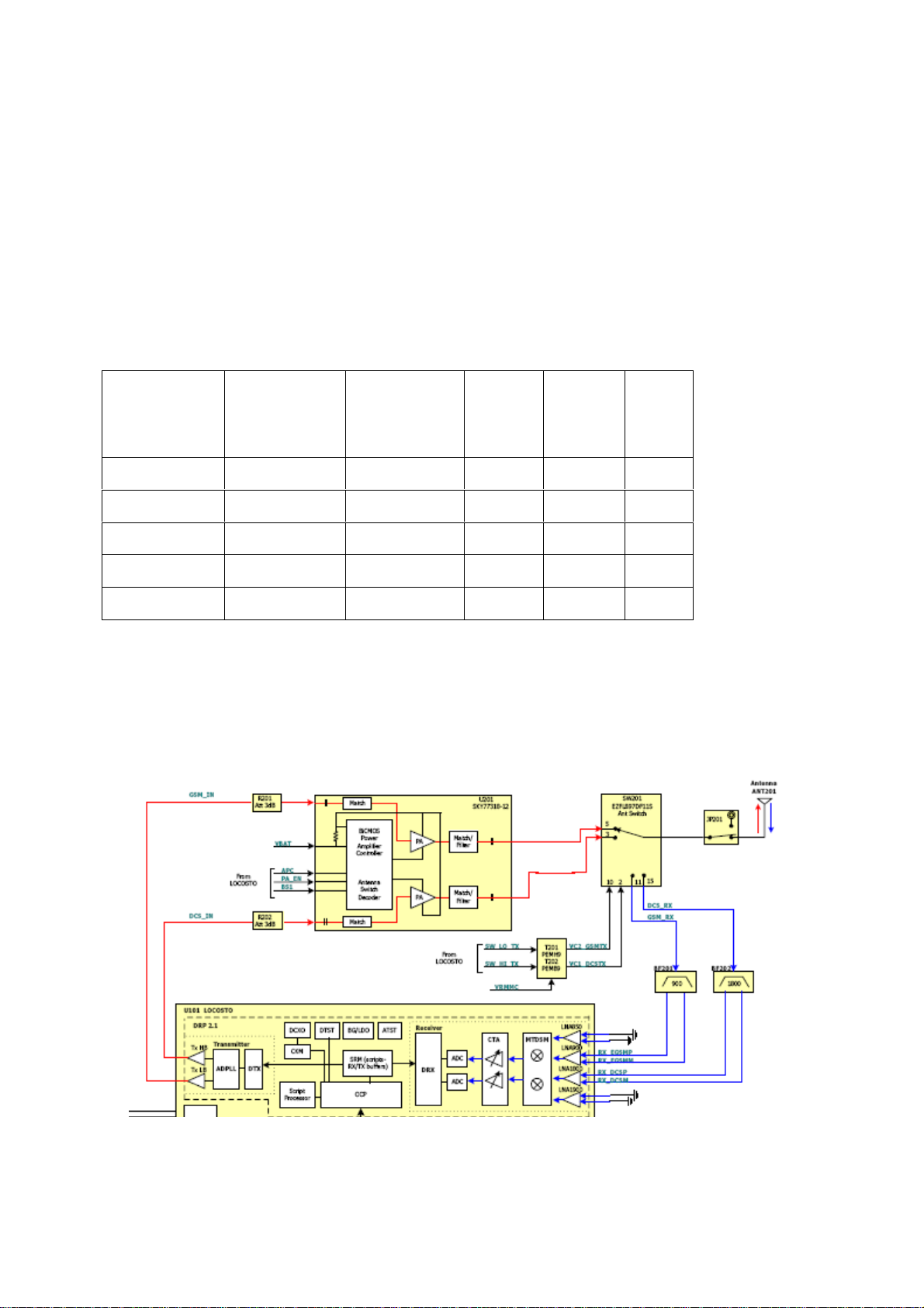
The radio frequency signal is received from internal PIFA-type antenna. Received
GSM RF sign al e nte rs t o PCB through the RF switch JP201. At this moment the T/R switch
SW201 is switched to RX mode to let the signal input to next stage. Then the signal goes
into SAW filter, BF201 and BF202 , which reject out-band signal and transfer the signal
from single-end to balanced. And the matching circuits between T/R switch and SAW
filter reduce the unwanted RF signal reflection and provide a flat frequency response in the
operation band. Finally the received signal will fed into Locosto Plus U101 DRP core
through a balanced MLCC matching network. The following table describes the control
voltages of T/R
SW_LO_TX
W375 EU
Standby Low x Low Low x
RX EGSM900 Low Low Low Low Low
RX DCS1800 Low Low Low Low High
TX GSM900 High High High High Low
TX DCS1800 High High High High High
switch. The low band (GSM900) RX received signal is transmitted from SW201 (Pin 11)
and input to low-band SAW filter BF201, while the high band (DCS1800) RX received
signal from SW201 (Pin 1) and then input to high-band SAW filter BF202. The last stage
of RX on PCB is Locosto U101 (Loocsto-Plus), and the DRP process will make the signal
into binary data.
PIN 5
of T201
SW_HI_TX
PIN 2
of T201
PA_EN
TP201
VAPC
PIN 20
of U201
BS1
TP202
switch and PA:
The RF signal
is received by
internal antenna
or by RF plug,
and the signal is
passing through
the RF switch
JP201 and then
fed into T/R
Figure 1: Locosto TX/RX Paths Description
Motorola Proprietary Information
- 4 -
W206/W213 Level 3 C
1.2 Locosto RX Mode
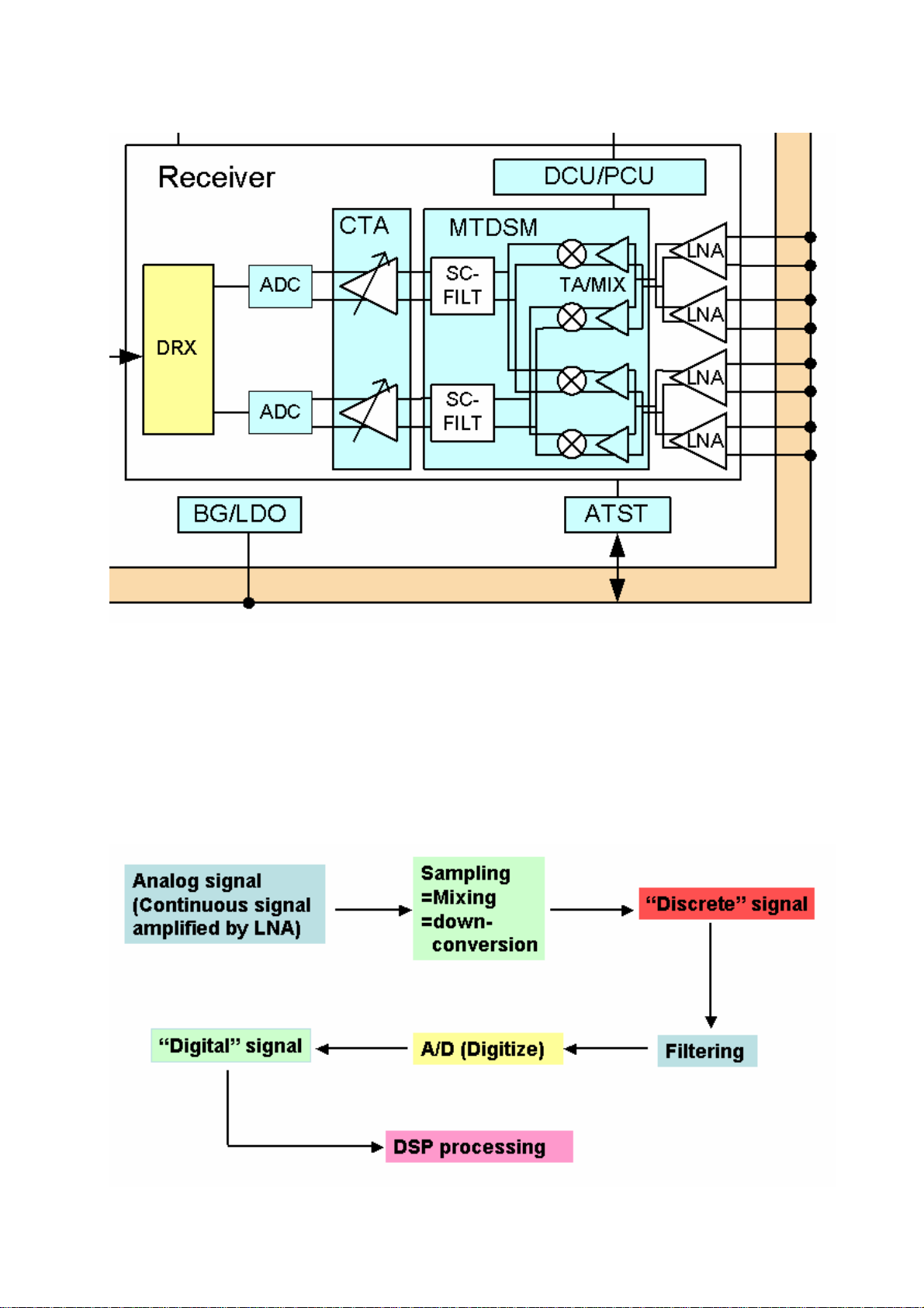
Figure 2: Locosto RX Signal Process
As described in Figure 2, when the RF signal is input to Locosto, it will be amplified by
a differential LNA in advance, in order to obtain a better NF in the last receiving stage.
And then it will be turned into discrete IF signal by a high-speed mixer. After passing
through a filter and an A/D converter, the discrete signal will become digital signal and
then input to Locosto core to do DSP process. The detail RX signal route is depicted as
below:
Motorola Proprietary Information
- 5 -
W206/W213 Level 3 C
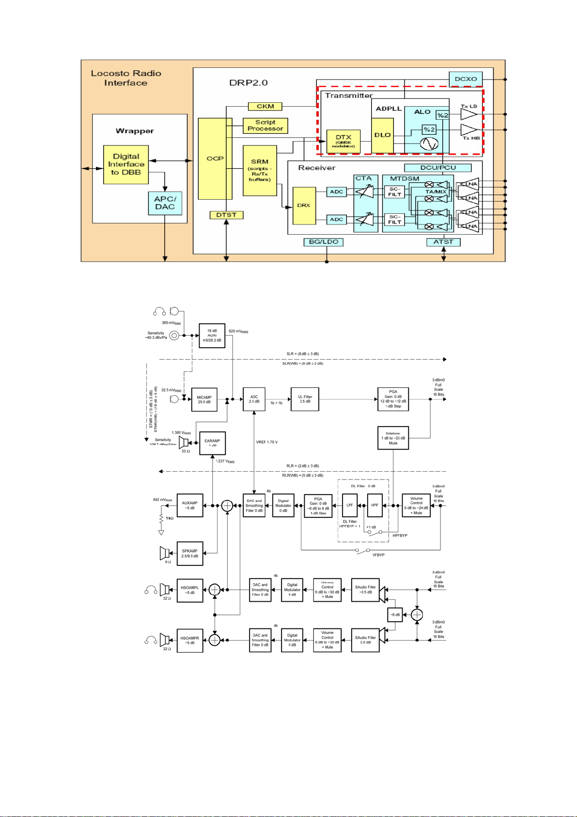
Figure 3: Baseband Downlink Block Diagram
Figure 3: Audio Codec Block Diagram
1.3 Audio Codec
The Audio codec consist of a voice codec dedicated to GSM application and an audio stereo
line. The voice codec circuitry processes analog audio components in the uplink path and
applies this signal to the voice signal interface for eventual baseband modulation. In the
Motorola Proprietary Information
- 6 -

W206/W213 Level 3 C
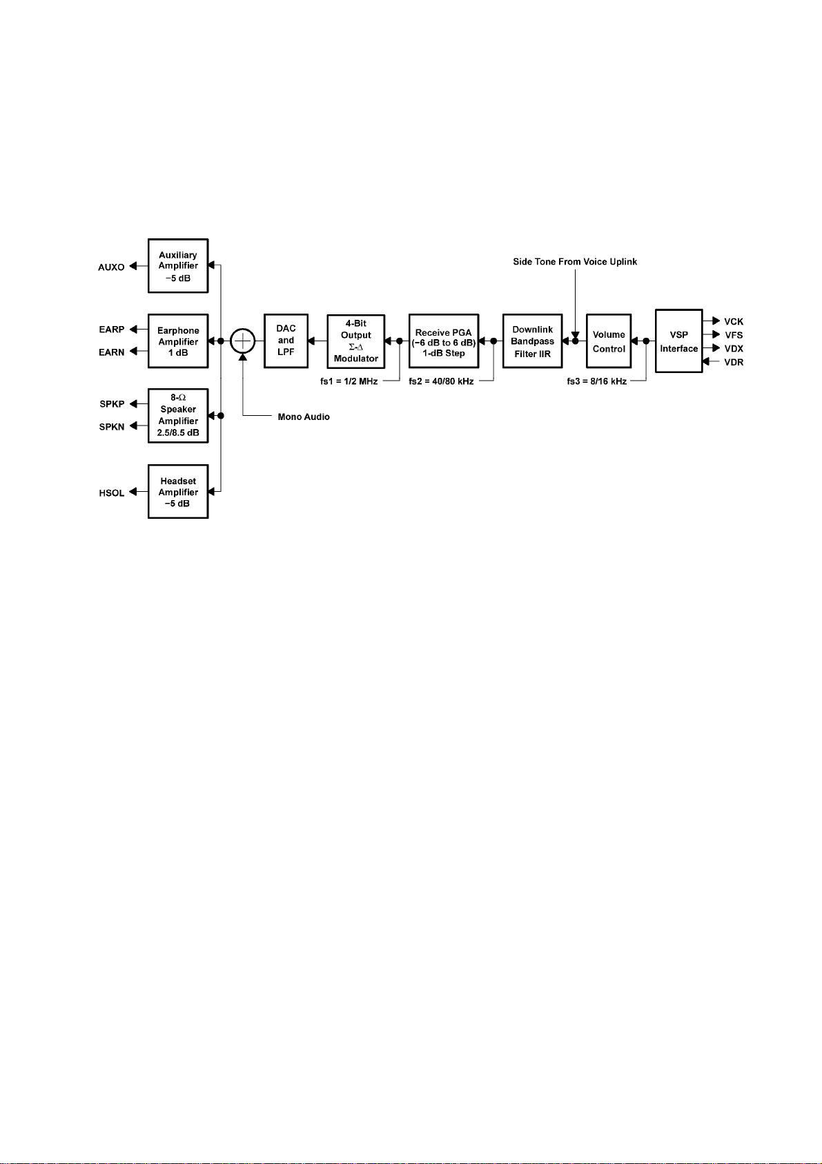
downlink path, the codec circuitry changes voice component data received from the voice
serial interface into analog audio. The voice codec support an 8/16 kHz sampling
frequency. The stereo audio path converts audio component data received from the I2S
serial interface into analog audio. The following paragraphs describe these
uplink/downlink and audio stereo functions in more details.
1.3.1 Voice Downlink Patch
The VDL path receives speech samples at the rate of 8 kHz from the Locosto-Plus IC U101
(DSP) via the VSP and converts them to analog signals to drive the external speech
transducer.
The digital speech coming from the Locosto-Plus IC U101 (DSP) is first fed to a speech
digital filter that has two functions. The first function is to interpolate the input signal and
to increase the sampling rate from 8 kHz up to 40 kHz to allow the digital-to-analog
conversion to be performed by an over-sampling digital modulator. The second function is
to band-limit the speech signal with both low-pass and high-pass transfer functions. The
filter, the PGA gain, and the volume gain can be bypassed by programming.
The interpolated and band-limited signal is fed to a second order Σ-∆ digital modulator
sampled at 1 MHz to generate a 4-bit (9 levels) over-sampled signal. This signal is then
passed through a dynamic element-matching block and then to a 4-bit digital-to-analog
converter (DAC).
Due to the over-sampling conversion, the analog signal obtained at the output of the 4–bit
DAC is mixed with a high frequency noise. Because a 4–bit digital output is used, a
first–order RC filter (included in the output stage) is enough to filter this noise.
The volume control and the programmable gain are performed in the TX digital filter.
Volume control is performed in steps of 6 dB from 0 dB to -24 dB. In mute state,
attenuation is higher than 40 dB. A fine adjustment of gain is possible from -6 dB to +6 dB
in 1–dB steps to calibrate the system depending on the earphone characteristics. The
earphone amplifier provides a full differential signal on the terminals EARP Triton-Lite Pin
J2 and EARN Triton-Lite Pin H2. The 8Ohm speaker amplifier provides a differential
signal on the terminals SPKP Triton-Lite Pin L6, K6 and SPKN Triton-Lite Pin M6, M7.
1.4 Earpiece Receiver
The Receiver
1.5 Headset
The headset uses a standard 2.5mm phone jack. The headset circuit contains analog
switches (U602 and U605), which are normally switched to receiver earpiece after power
on. When system turns on, the signal HS_EN (U101 Pin T3) are applied. When earphone
plug in, the phone will detect this action and make an appropriate response to answer a
call while incoming call occur. The interrupt for the headphones is detected on the
HS_DETECT (U101 Pin C6) line from Pin 6 of Headset Jack J602. This signal will be
pulled to high when the headset is connected.
1.6 Speaker Phone
When the handset set the hand-free mode, the Triton-Lite will switch from EARP/EARN
to SPKP/SPKN trace and receiver signal will be through Audio amplifier U601 to Speaker.
J10 is connected to EARP Triton-Lite Pin J2 and EARN Triton-Lite Pin H2.
Motorola Proprietary Information
- 7 -
W206/W213 Level 3 C
1.7 Data Download Receive Path
The External download cable is connected to the Earphone Jack J602, the headset
connector of the mobile phone. The download path is routed from J602 Pin 2 via U602
Pin 1 and U607 Pin C1 to RX_Modem. The RX_Modem signal connects to
Locosto-Plus IC U101 Pin L7 to provide this capability. When software is set to download
mode, the signal HS_EN (U101 Pin T3) is applied high, the phone will entered to
download state till download cable pulls out.
Figure 4: Voice Codec Downlink Patch
1.8 FM radio (only available for W213)
The headphone antenna (J602) is used with a standard 2.5mm phone jack. Silicon Lab
Si4702 (U202) demodulated the FM radio. The left and right audio channels are driven by
Triton_Lite (U103) audio amplifier onto left and right audio path and common audio
connector is used for the audio return path and FM antenna.
2 Transmit
2.1 Audio (Voice uplink Patch)
The VUL path includes two input stages. The first stage is a microphone amplifier,
compatible with electric microphones containing a FET buffer with open drain output. The
microphone amplifier has a gain of typically 25.6 dB (±1 dB) and provides an external
voltage of 2.5V to bias the microphone (HS_BIAS Locosto-Plus Pin K8).
The auxiliary audio input can be used as an alternative source for higher-level speech
signals. This stage performs single-ended conversion and provides a programmable gain
of 4.6 dB or 28.2 dB. The third stage is a headset microphone amplifier, compatible with
electric microphones. The headset microphone amplifier has a gain of typically 18 dB and
provides an external voltage of 2.0V or 2.5V to bias the headset microphone (HS_BIAS
Locosto-Plus Pin K8). When one of the input stages (HSMIC) is in use, the other input
stages are disabled and powered down.
The resulting fully differential signal is fed to the analog-to-digital converter (ADC). The
ADC conversion slope depends on the value of the internal voltage reference.
Motorola Proprietary Information
- 8 -
 Loading...