

Motorola VN2222LL Datasheet
SEMICONDUCTOR TECHNICAL DATA
N–Channel — Enhancement
MAXIMUM RATINGS
Rating Symbol Value Unit
Drain–Source Voltage V
Drain–Gate Voltage (RGS = 1.0 MΩ) V
Gate–Source Voltage
— Continuous
— Non–repetitive (tp ≤ 50 µs)
Drain Current
Continuous
Pulsed
Total Power Dissipation @ TA = 25°C
Derate above 25°C
Operating and Storage
T emperature Range
DSS
DGR
V
V
GSM
I
DM
P
TJ, T
GS
I
D
D
stg
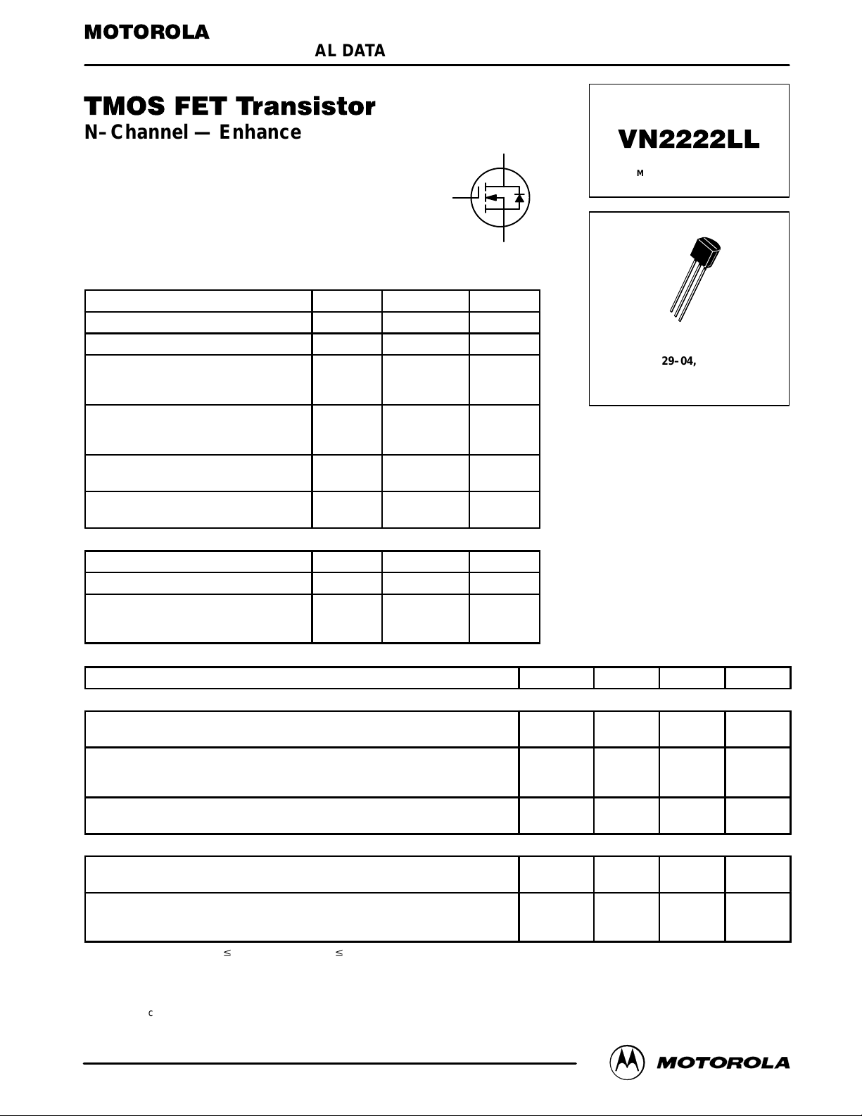
3 DRAIN
2
GATE
60 Vdc
60 Vdc
±20
±40
150
1000
400
3.2
–55 to +150 °C
Vdc
Vpk
mAdc
mW
mW/°C
1 SOURCE
Order this document
by VN2222LL/D
Motorola Preferred Device
1
2
3
CASE 29–04, STYLE 22
TO–92 (TO–226AA)
THERMAL CHARACTERISTICS
Characteristic Symbol Max Unit
Thermal Resistance, Junction to Ambient R
Maximum Lead Temperature for
Soldering Purposes, 1/16″ from case
for 10 seconds
ELECTRICAL CHARACTERISTICS (T
Characteristic Symbol Min Max Unit
θJA
T
L
= 25°C unless otherwise noted)
C
OFF CHARACTERISTICS
Drain–Source Breakdown Voltage
(VGS = 0, ID = 100 µAdc)
Zero Gate Voltage Drain Current
(VDS = 48 Vdc, VGS = 0)
(VDS = 48 Vdc, VGS = 0, TJ = 125°C)
Gate–Body Leakage Current, Forward
(V
= 30 Vdc, VDS = 0)
GSF
ON CHARACTERISTICS
Gate Threshold Voltage
(VDS = VGS, ID = 1.0 mAdc)
Static Drain–Source On–Resistance
(VGS = 10 Vdc, ID = 0.5 Adc)
(VGS = 10 Vdc, ID = 0.5 Vdc, TC = 125°C)
1. Pulse Test: Pulse Width v 300 µs, Duty Cycle v 2.0%.
(1)
312.5 °C/W
300 °C
V
(BR)DSS
I
DSS
I
GSSF
V
GS(th)
r
DS(on)
60 — Vdc
—
—
— –100 nAdc
0.6 2.5 Vdc
—
—
10
500
7.5
13.5
µAdc
Ω
Preferred devices are Motorola recommended choices for future use and best overall value.
REV 1
Motorola Small–Signal Transistors, FETs and Diodes Device Data
Motorola, Inc. 1997
1
VN2222LL
)
f = 1.0 MHz)
(
DD
,
D
,
ELECTRICAL CHARACTERISTICS
ON CHARACTERISTICS
Drain–Source On–Voltage
(VGS = 5.0 Vdc, ID = 200 mAdc)
(VGS = 10 Vdc, ID = 500 mAdc)
On–State Drain Current
(VGS = 10 Vdc, VDS ≥ 2.0 V
Forward Transconductance
(VDS = 10 Vdc, ID = 500 mAdc)
(1)
(Continued)
DS(on)
(TC = 25°C unless otherwise noted) (Continued)
Characteristic Symbol Min Max Unit
)
DYNAMIC CHARACTERISTICS
Input Capacitance
Output Capacitance
Reverse Transfer Capacitance
SWITCHING CHARACTERISTICS
Turn–On Delay Time
Turn–Off Delay Time
1. Pulse Test: Pulse Width v 300 µs, Duty Cycle v 2.0%.
(1)
(VDS = 25 Vdc, VGS = 0,
(VDD = 15 Vdc, ID = 600 mA,
R
= 25 Ω, RL = 23 Ω)
gen
f = 1.0 MHz
V
DS(on)
I
D(on)
g
C
C
C
t
t
fs
iss
oss
rss
on
off
—
—
750 — mA
100 — µmhos
— 60
— 25
— 5.0
— 10
— 10
1.5
3.75
Vdc
pF
ns
2
Motorola Small–Signal Transistors, FETs and Diodes Device Data
 Loading...