

Motorola TP3061 Datasheet
1
TP3061MOTOROLA RF DEVICE DATA
The RF Line
The TP3061 is designed for 960 MHz mobile base stations in both analog and
digital applications. It incorporates high value emitter ballast resistors, gold
metallizations and offers a high degree of reliability and ruggedness. Including
double input and output matching networks, the TP3060 features high
impedances and is easy to match.
• Motorola Advanced Amplifier Concept Package
• Oxynitride Passivation
• Specified 26 Volts, 960 MHz Characteristics
Output Power = 45 Watts
Minimum Gain = 8.0 dB
Efficiency = 50%
• Circuit board photomaster available upon request by contacting
RF Tactical Marketing in Phoenix, AZ.
MAXIMUM RATINGS
Rating Symbol Value Unit
Collector–Emitter Voltage V
CER
40 Vdc
Collector–Base Voltage V
CBO
48 Vdc
Emitter–Base Voltage V
EBO
4.0 Vdc
Collector Current — Continuous I
C
10 Adc
Total Device Dissipation @ TC = 25°C
Derate above 25°C
P
D
175
1.0
Watts
W/°C
Storage Temperature Range T
stg
–65 to +150 °C
Operating Junction Temperature T
J
200 °C
THERMAL CHARACTERISTICS
Characteristic Symbol Max Unit
Thermal Resistance, Junction to Case (1) at 70°C Case R
θJC
1.2 °C/W
ELECTRICAL CHARACTERISTICS (T
C
= 25°C unless otherwise noted.)
Characteristic
Symbol Min Typ Max Unit
OFF CHARACTERISTICS
Collector–Emitter Breakdown Voltage
(IC = 60 mA, RBE = 75 Ω)
V
(BR)CER
40 — — Vdc
Emitter–Base Breakdown Voltage
(IC = 6.0 mAdc)
V
(BR)EBO
3.5 — — Vdc
Collector–Base Breakdown Voltage (IE = 60 mAdc) V
(BR)CBO
48 — — Vdc
Collector–Emitter Leakage (VCE = 26 V, RBE = 75 Ω) I
CER
— — 15 mA
NOTE: (continued)
1. Thermal resistance is determined under specified RF operating condition.
Order this document
by TP3061/D
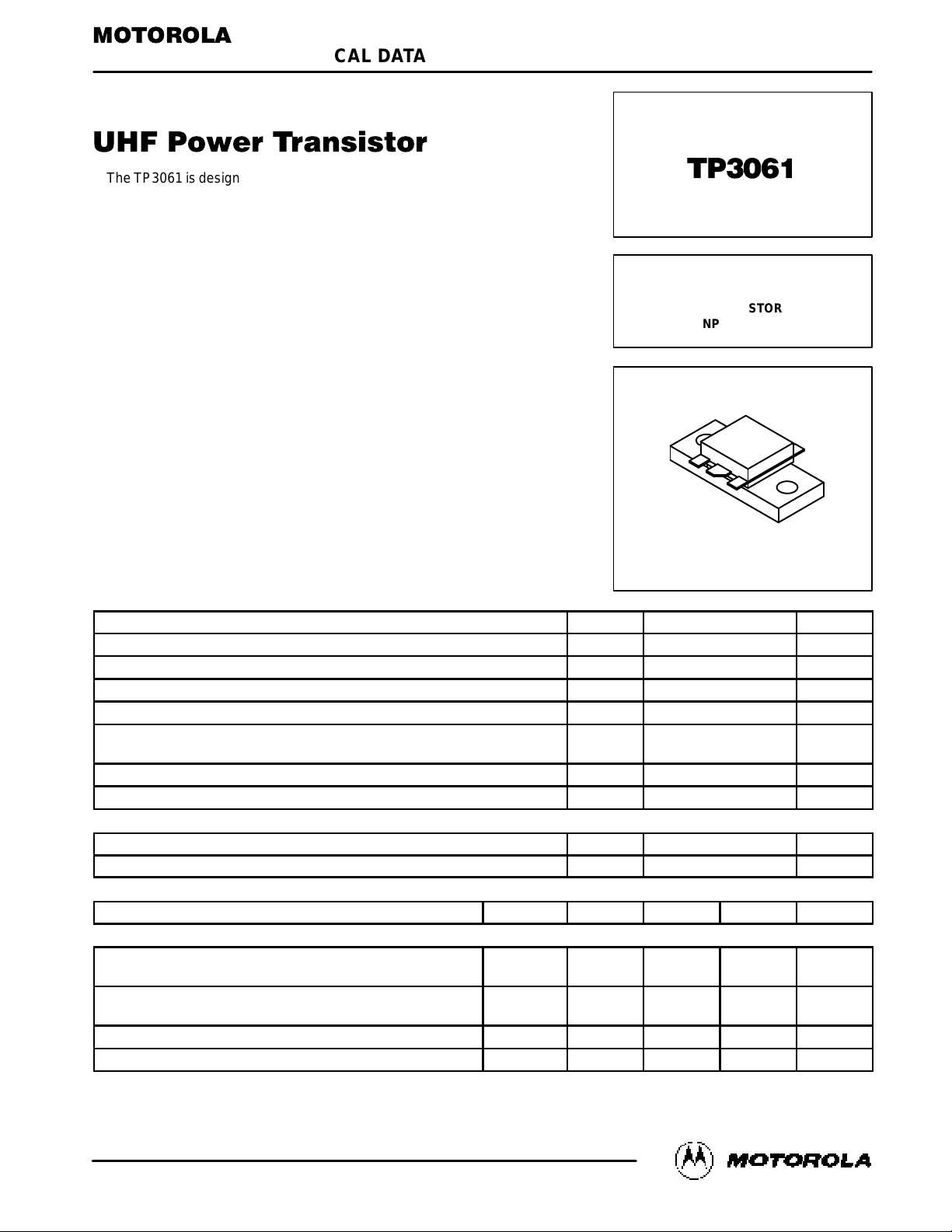
SEMICONDUCTOR TECHNICAL DATA
45 W, 960 MHz
UHF POWER
TRANSISTOR
NPN SILICON
CASE 333A–02, STYLE 2
Motorola, Inc. 1994
REV 6
TP3061
2
MOTOROLA RF DEVICE DATA
ELECTRICAL CHARACTERISTICS — continued (T
C
= 25°C unless otherwise noted.)
Characteristic
Symbol Min Typ Max Unit
ON CHARACTERISTICS
DC Current Gain
(IC = 1.0 Adc, VCE = 10 Vdc)
h
FE
15 — 100 —
DYNAMIC CHARACTERISTICS
Output Capacitance (2)
(VCB = 26 V, IE = 0, f = 1.0 MHz)
C
ob
45 60 — pF
FUNCTIONAL TESTS
Common–Emitter Amplifier Power Gain
(VCC = 26 V, P
out
= 45 W, ICQ = 200 mA, f = 960 MHz)
G
p
8.0 8.8 — dB
Collector Efficiency
(VCC = 26 V, P
out
= 45 W, f = 960 MHz)
η 50 53 — %
Load Mismatch
(VCC = 26 V, P
out
= 45 W, ICQ = 200 mA,
Load VSWR = 5:1, at all phase angles)
ψ
No Degradation in Output Power
Before and After Test
Overdrive
(VCC = 26 V, Pin = 15 W, f = 960 MHz)
OD
No Degradation in Output Power
NOTE:
2. Value of “Cob” is that of die only. It is not measurable in TP3061 because of internal matching network.
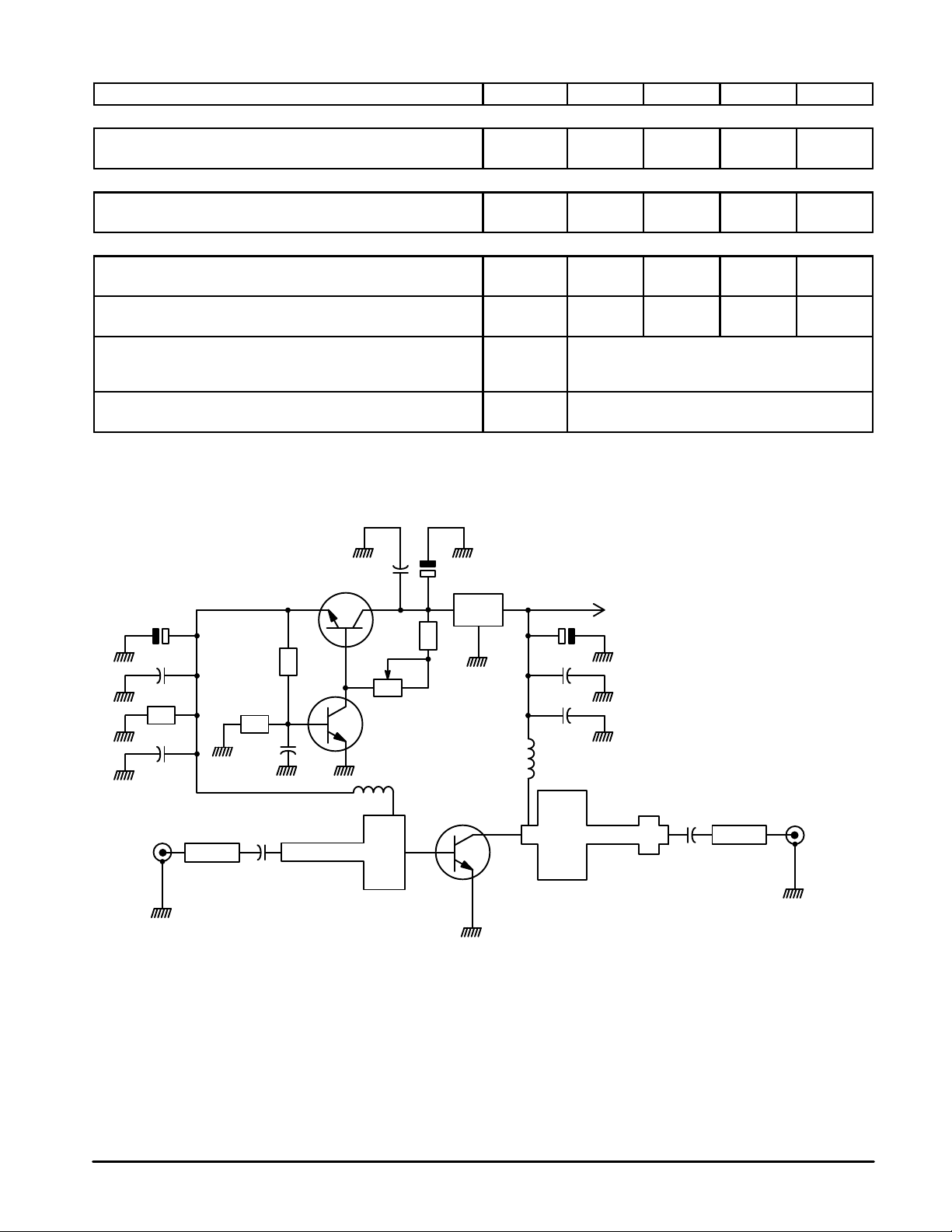
Figure 1. 960 MHz Test Circuit
C1, C4, C7, C12 — Capacitor Chip 0805 330 pF 5%
C2 — Capacitor Chip 82 pF ATC
C5, C11, C8 — Capacitor Chip 0805 15 nF 5%
C6, C9, C10 — Capacitor Chip 0805 6.0, 8.0 µF 35 V
L1, L2 — 1.5 Turns #18 AWG Choke
R1 — Chip Resistor 47 Ω 1206 5%
R2 — Chip Resistor 270 Ω 0805 5%
R3 — Chip Resistor 47 Ω 0805 5%
R4 — Chip Resistor 100 Ω 0805 5%
R5 — Trimmer 1.0 kΩ
T1 — SMD Transistor MJD31C or Similar
T2 — SMD Transistor
T3 — Voltage Regulator 7805
Board Material — 1/50″, Teflon Glass, εr = 2.5,
Cu Clad 2 Sides, 35 µm Thick
RF INPUT
50
Ω
RF OUTPUT
50
Ω
D.U.T.
+V
CC
++
R3
C10
C11
C12
C6
C5
R1
C4
R2
C7
T1
C1
L2
L1
R5
C6
T3
C8 C9
R4
C2
T2
+
 Loading...