

Motorola TP3032 Datasheet
1
TP3032MOTOROLA RF DEVICE DATA
The RF Line
The TP3032 is designed for 26 volts, common emitter, 960 MHz base station
amplifiers, for use in analog and digital systems.
• Specified 26 Volts, 960 MHz Characteristics
Output Power — 21 Watts
Gain — 7.5 dB min
• Silicon Nitride Passivated
• Gold Metallized, Emitter Ballasted for Long Life and Resistance to
Metal Migration
• Class AB Operation
• Circuit board photomaster available upon request by contacting
RF Tactical Marketing in Phoenix, AZ.
MAXIMUM RATINGS
Rating Symbol Value Unit
Collector–Emitter Voltage V
CER
40 Vdc
Collector–Base Voltage V
CBO
48 Vdc
Emitter–Base Voltage V
EBO
3.5 Vdc
Collector–Current — Continuous I
C
4 Adc
Total Device Dissipation @ TC = 25°C
Derate above 25°C
P
D
52.5
0.3
Watts
W/°C
Storage Temperature Range T
stg
– 65 to +150 °C
Operating Junction Temperature T
J
200 °C
THERMAL CHARACTERISTICS
Characteristic Symbol Max Unit
Thermal Resistance, Junction to Case (1) R
θJC
3.3 °C/W
ELECTRICAL CHARACTERISTICS (T
C
= 25°C unless otherwise noted.)
Characteristic
Symbol Min Typ Max Unit
OFF CHARACTERISTICS
Collector–Emitter Breakdown Voltage
(IC = 30 mA, RBE = 75 Ω)
V
(BR)CER
40 — — Vdc
Emitter–Base Breakdown Voltage
(IE = 5 mAdc)
V
(BR)EBO
3.5 — — Vdc
Collector–Base Breakdown Voltage
(IC = 30 mAdc)
V
(BR)CBO
48 — — Vdc
Collector–Emitter Leakage
(VCE = 26 V, RBE = 75 Ω)
I
CER
— — 8 mA
ON CHARACTERISTICS
DC Current Gain
(IC =1 Adc, VCE = 10 Vdc)
h
FE
15 — 80 —
NOTE: (continued)
1. Thermal resistance is determined under specified RF operating condition.
Order this document
by TP3032/D
SEMICONDUCTOR TECHNICAL DATA
21 W, 960 MHz
RF POWER TRANSISTOR
NPN SILICON
CASE 319–07, STYLE 2
Motorola, Inc. 1994
REV 6
TP3032
2
MOTOROLA RF DEVICE DATA
ELECTRICAL CHARACTERISTICS — continued (T
C
= 25°C unless otherwise noted.)
Characteristic
Symbol Min Typ Max Unit
DYNAMIC CHARACTERISTICS
Output Capacitance
(VCB = 26 V, IE = 0, f = 1 MHz )
C
ob
— 30 — pF
FUNCTIONAL TESTS
Common–Emitter Amplifier Gain
(VCC = 26 V, P
out
= 21 W, ICQ = 100 mA, f = 960 MHz)
G
p
7.5 8.5 — dB
Load Mismatch
(VCC = 26 V, P
out
= 21 W, ICQ = 100 mA, Load VSWR = 5:1, at
All Phase Angles at Frequency of Test)
ψ
No Degradation in Output Power
Collector Efficiency
(VCC = 26 V, P
out
= 21 W, f = 960 MHz)
η 50 55 — %
Over Drive
(VCC = 26 V, Pin = 6 W, f = 960 MHz)
OD
No Degradation in Output Power
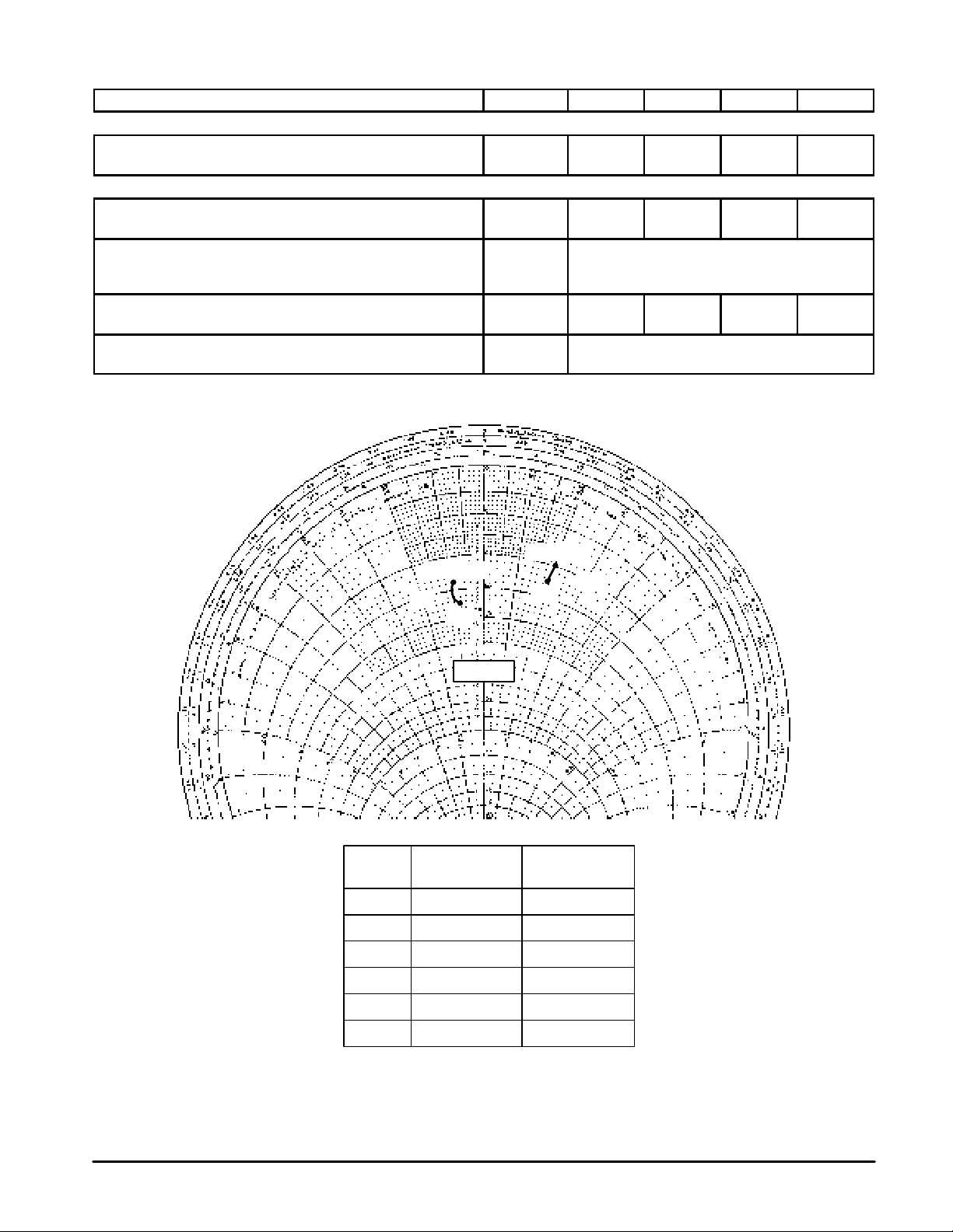
860 2.9 – j0.4 2 + j2.2
Figure 1. Series Equivalent Input and Output Impedances
f
(MHz)
Z
in
(Ω)
ZOL*
(Ω)
ZOL* = Conjugate of optimum load impedance
ZOL* = into which the device operates at a given
ZOL* = output power, voltage, current and frequency.
VCE = 26 V P
out
= 21 W
880
900
935
960
980
2.9 – j0.9
2.9 – j1.45
3.25 – j1.5
3.2 – j0.95
3.55 – j1.1
2.1 + j2.2
2.25 + j2.5
2.4 + j2.3
2.5 + j2
2.6 + j2.15
f = 860 MHz
Z
in
980
f = 860 MHz
980
ZOL*
Zo = 10
Ω
 Loading...