

Motorola SAA1042V Datasheet
Order this document by SAA1042/D
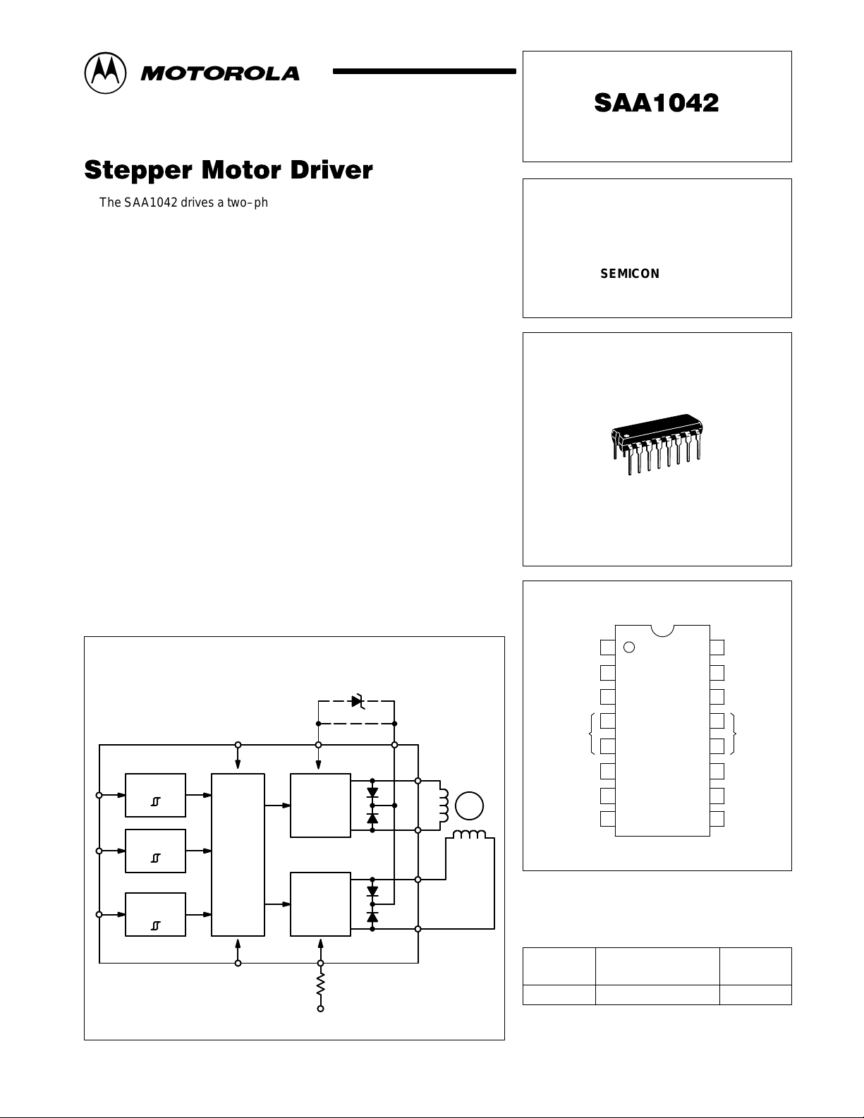
The SAA1042 drives a two–phase stepper motor in the bipolar mode. The
device contains three input stages, a logic section and two output stages.
The IC is contained in a 16 pin dual–in–line heat tab plastic package for
improved heatsinking capability . The center four ground pins are connected
to the copper alloy heat tab and improve thermal conduction from the die to
the circuit board.
• Drive Stages Designed for Motors: 6.0 V and 12 V: SAA1042V
• 500 mA/Coil Drive Capability
• Built–In Clamp Diodes for Overvoltage Suppression
• Wide Logic Supply Voltage Range
• Accepts Commands for CW/CCW and Half/Full Step Operation
• Inputs Compatible with Popular Logic Families: MOS, TTL, DTL
• Set Input Defined Output State
• Drive Stage Bias Adaptable to Motor Power Dissipation for
Optimum Efficiency
STEPPER MOTOR
DRIVER
SEMICONDUCTOR
TECHNICAL DATA
16
1
V SUFFIX
PLASTIC PACKAGE
CASE 648C
PIN CONNECTIONS
Figure 1. Representative Block Diagram
7
10
8
Clock
CW/CCW
Full/
Half Step
V
CC
11
Logic
Gnd
9
V
M
Driver
Driver
R
B
MOTOROLA ANALOG IC DEVICE DATA
V
Z
15
6
Driver Bias
Set
A
L2
1
VD VM
2
3
L1
4
VD
2
3
M
1L1L2
16
L3
L4
14
Gnd Gnd
5
Set/
Clock
Step
6
7
8
(Top View)
Driver Bias
Full/Half
16
15
14
13
12
11
10
9
L3
L4
V
CC
CW/CCW
Gnd
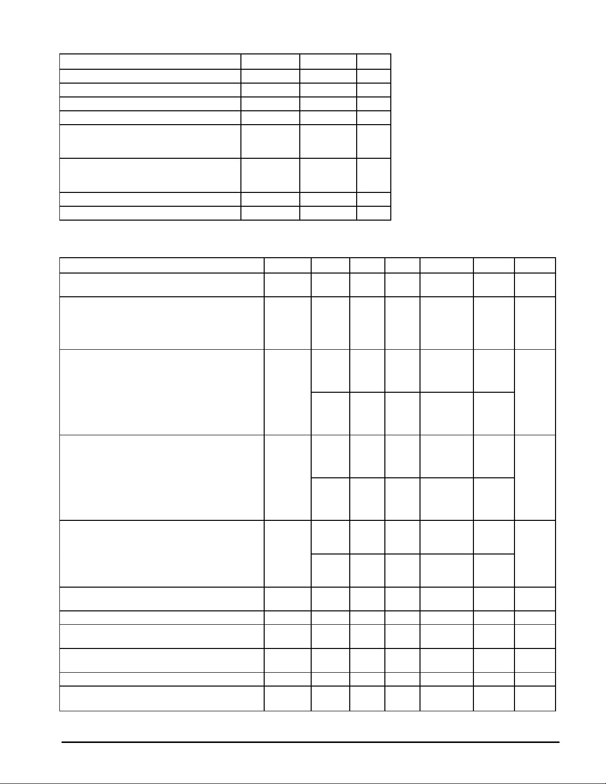
ORDERING INFORMATION
Operating
Device
SAA1042V TJ = – 30° to +125°C Plastic DIP
Motorola, Inc. 1996 Rev 2
Temperature Range
Package
1
SAA1042
MAXIMUM RATINGS
Clamping Voltage (Pins 1, 3, 14, 16) V
Over Voltage (VOV = V
Supply Voltage V
Switching or Motor Current/Coil I
Input Voltage (Pins 7, 8, 10) Vin clock
Power Dissipation (Note 1)
Thermal Resistance, Junction–to–Air
Thermal Resistance, Junction–to–Case
Operating Junction Temperature Range T
Storage Temperature Range T
NOTE: 1. The power dissipation (PD) of the circuit is given by the supply voltage (VM and VCC) and the
motor current (IM), and can be determined from Figures 3 and 5. PD = P
ELECTRICAL CHARACTERISTICS (T
Supply Current 11 I
Motor Supply Current
(I
= –400 µA, Pins 1, 3, 14, 16 Open)
Pin 6
VM = 6.0 V
VM = 12 V
VM = 24 V
Input Voltage, High State
Input Voltage, Low State V
Input Reverse Current, High State
(Vin = VCC)
Input Forward Current, Low State
(Vin = Gnd)
Output Voltage, High State (VM = 12 V)
I
= –500 mA
out
I
= –50 mA
out
Output Voltage, Low State
I
= 500 mA
out
I
= 50 mA
out
Output Leakage Current, Pin 6 = Open
(VM = VD = V
Clamp Diode Forward Voltage (Drop at IM = 500 mA) 2 V
Clock Frequency 7 f
Clock Pulse Width 7 t
Set Pulse Width 6 t
Set Control Voltage, High State
Set Control Voltage, Low State
(TA = 25°C, unless otherwise noted.)
Rating Symbol SAA1042V Unit
clamp
– VM) V
clamp
= 25°C, unless otherwise noted.)
A
Characteristics Pin(s) Symbol V
clamp max
)
OV
CC
M
Vin Full/Half
Vin CW/CCW
P
D
θJA
θJC
J
stg
15 I
7, 8, 10
7, 8, 10
1, 3, 14, 16
1, 3, 14, 16 I
6 — — V
20 V
6.0 V
20 V
500 mA
V
CC
2.0
80
15
–30 to +125 °C
–65 to +150 °C
– P
drive
CC
M
V
IH
IL
I
IR
I
IF
V
OH
V
OL
DR
F
c
w
s
V
W
°C/W
logic.
CC
5.0 V
20 V
5.0 V
5.0 V
5.0 V
5.0 V
10 V
15 V
20 V
5.0 V
10 V
15 V
20 V
5.0 V
10 V
15 V
20 V
5.0 V
10 V
15 V
20 V
5.0 –
20 V
5.0 –
20 V
5.0 –
20 V
— — 2.5 3.5 V
5.0 –
20 V
5.0 –
20 V
— 10 — — µs
Min Typ Max Unit
—
—
—
—
—
2.0
7.0
10
14
—
—
—
—
—
—
—
—
–10
–25
–40
–50
—
—
—
—
–100 — — µA
0 — 50 kHz
10 — — µs
M
—
—
—
25
30
40
—
—
—
—
—
—
—
—
—
—
—
—
—
—
—
—
VM – 2.0
VM – 1.2
0.7
0.2
—
—
3.5
8.5
—
—
—
—
—
—
—
0.8
1.5
2.5
3.5
2.0
2.0
3.0
5.0
—
—
—
—
—
—
—
—
—
0.5
mA
mA
µA
V
V
V
2
MOTOROLA ANALOG IC DEVICE DATA
 Loading...