

Motorola MPSH69 Datasheet
1
Motorola Small–Signal Transistors, FETs and Diodes Device Data
PNP Silicon
MAXIMUM RATINGS
Rating Symbol Value Unit
Collector–Emitter Voltage V
CEO
–15 Vdc
Collector–Base Voltage V
CBO
–15 Vdc
Emitter–Base Voltage V
EBO
–4.0 Vdc
Total Device Dissipation @ TA = 25°C
Derate above 25°C
P
D
350
2.81
mW
mW/°C
Operating and Storage Junction
Temperature Range
TJ, T
stg
–55 to +150 °C
THERMAL CHARACTERISTICS
Characteristic Symbol Max Unit
Thermal Resistance, Junction to Ambient
R
q
JA
357 °C/W
ELECTRICAL CHARACTERISTICS (T
A
= 25°C unless otherwise noted)
Characteristic
Symbol Min Typ Max Unit
OFF CHARACTERISTICS
Collector–Emitter Breakdown Voltage
(IC = –1.0 mAdc, IB = 0)
V
(BR)CEO
–15 — — Vdc
Collector–Base Breakdown Voltage
(IC = –10 mAdc, IE = 0)
V
(BR)CBO
–15 — — Vdc
Emitter–Base Breakdown Voltage
(IE = –10 mAdc, IC = 0)
V
(BR)EBO
–4.0 — — Vdc
Collector Cutoff Current
(VCB = –10 Vdc, IE = 0)
I
CBO
— — –100 nAdc
Preferred devices are Motorola recommended choices for future use and best overall value.
Order this document
by MPSH69/D
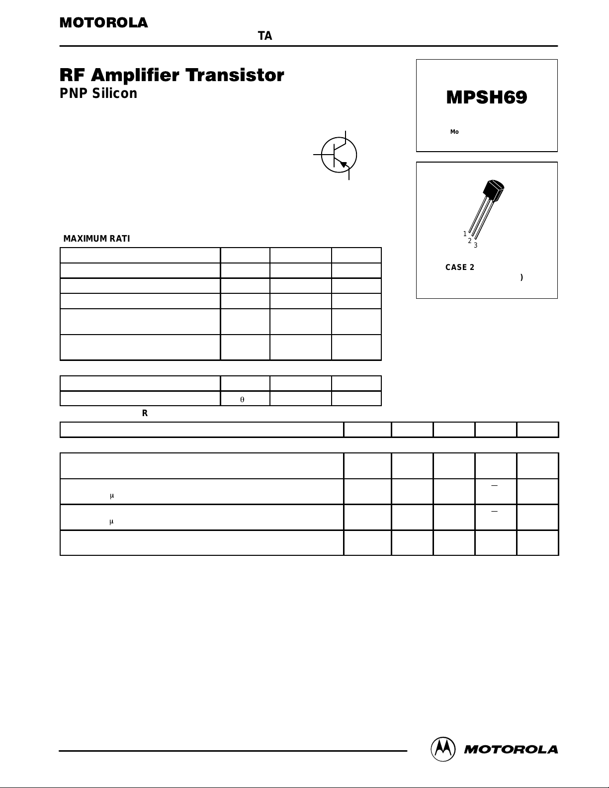
SEMICONDUCTOR TECHNICAL DATA
CASE 29–04, STYLE 1
TO–92 (TO–226AA)
1
2
3
Motorola Preferred Device
Motorola, Inc. 1996
COLLECTOR
3
2
BASE
1
EMITTER
MPSH69
2
Motorola Small–Signal Transistors, FETs and Diodes Device Data
ELECTRICAL CHARACTERISTICS
(TA = 25°C unless otherwise noted) (Continued)
Characteristic
Symbol Min Typ Max Unit
ON CHARACTERISTICS
DC Current Gain
(IC = –10 mAdc, VCE = –10 Vdc)
h
FE
30 — 300 —
SMALL–SIGNAL CHARACTERISTICS
Current–Gain — Bandwidth Product
(IC = –10 mAdc, VCE = –10 Vdc, f = 100 MHz)
f
T
2000 — — MHz
Collector–Base Capacitance
(VCE = –10 Vdc, IE = 0, f = 1.0 MHz)
C
cb
— — 0.3 pF
 Loading...