

Motorola MPC2105P, MPC2104P, MPC2104PDG66, MPC2105PDG66 Datasheet

MPC2104P•MPC2105P
1
MOTOROLA FAST SRAM
Product Preview
256KB/512KB BurstRAM
Secondary Cache Modules for
PowerPC PReP/CHRP Platforms
The MPC2104P (256KB) and MPC2105P (512KB) are designed to provide
burstable, high performance L2 cache for the PowerPC 60x microprocessor family
in conformance with the PowerPC Reference Platform (PReP) and the PowerPC
Common Hardware Reference Platform (CHRP) specifications.
The MPC2104P and MPC2105P utilize synchronous BurstRAMs. The MPC2104P
module is configured as 32K x 64 bits and uses two of the 3.3 V 32K x 32 data RAMs.
The MPC2105P is configured as 64K x 64 bits and uses two of the 3.3 V 64K x 32
data RAMs. Both modules are in a 178 (89 x 2) pin DIMM format. For tag bits on the
2104P, a 5 V cache tag RAM configured as 8K x 14 for tag field plus 8K x 2 for valid
and dirty status bits is used. For tag bits on the 2105P, a 5 V cache tag RAM
configured as 16K x 14 for tag field plus 16K x 2 for valid and dirty status bits is used.
Bursts can be initiated with the ADS
signal. Subsequent burst addresses are
generated internally to the BurstRAM by the CNTEN
signal.
Write cycles are internally self–timed and are initiated by the rising edge of the clock
(CLKx) inputs. Writes are global with two inputs for reduced loading.
Presence detect pins are available for auto configuration of the cache control.
The module family pinout will support 5 V and 3.3 V components for a clear path
to lower voltage and power savings. Both power supplies must be connected.
All of these cache modules are plug and pin compatible with each other.
• PowerPC–Style Burst Counter On Chip
• Pipeline Data I/O
• Plug and Pin Compatibility
• Multiple Clock Pins for Reduced Loading
• All Cache Data and Tag I/Os are LVTTL (3.3 V) Compatible
• Three State Outputs
• Buffered Addresses to Data RAMs for Reduced Loading
• Fast Module Clock Rates: Up to 66 MHz
• Fast SRAM Access Times: 9 ns for Tag RAM Match
8 ns for Data RAM
• Decoupling Capacitors for Each Fast Static RAM
• High Quality Multi–Layer FR4 PWB With Separate Power and Ground Planes
• 178 Pin Card Edge Module
• Burndy Connector, Part Number: ELF178KSC–3Z50
BurstRAM is a trademark of Motorola.
The PowerPC name is a trademark of IBM Corp., used under license therefrom.
This document contains information on a new product under development. Motorola reserves the right to change or discontinue this product without notice.
Order this document
by MPC2104P/D
MOTOROLA
SEMICONDUCTOR TECHNICAL DATA
MPC2104P
MPC2105P
REV 2
12/20/96
Motorola, Inc. 1996
MPC2104P•MPC2105P
2
MOTOROLA FAST SRAM
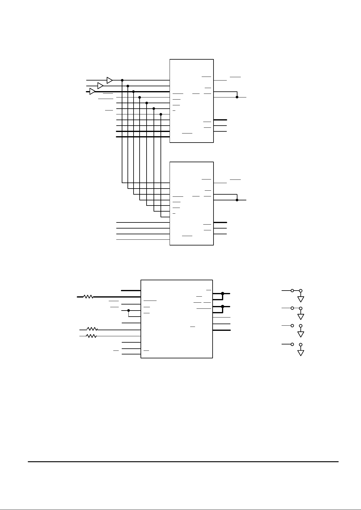
MPC2104P BLOCK DIAGRAM
32K x 32 SRAM
ADSC
ADV
SA1
ADS0
SA0
SA
A27
CWE0
A14 – A26
SBa – SBd
SW
SGW
PD3
PD2
PD1
PD0
J2
J0
J3
A14 – A26
A0 – A13
TCLR
TWE
CLK2
MATCH
VALIDIN
DIRTYIN
TG
TAG: 16K x 14 + V + D
A0 – A12
RESET
TDQ0 – TDQ13
TAH, TAG
, TAD
SFUNC, GS, A13
WS
WT
K
VALIDD
DIRTYD
GT
TT1, E1
E2, PWRDN
V
SS
VCC via 100
Ω
TA, VALIDQ
V
CCQ
V
DD
NC
MATCH
DIRTYOUT
DIRTYQ
J1
V
CC
V
CC
V
DD
ZZ
G
V
DD
SE1
K
CG0
DH0 – DH31
STANDBY
BURSTMODE
CLK0
SE3
LBO
DQa – DQd
SE2, ADSP
A28
CNTEN0
V
SS
V
SS
VDD via 100
Ω
V
DD
CLK1
V
SS
VDD via 100
Ω
V
DD
16244
32K x 32 SRAM
ADSC
ADV
SA1
SA0
SA
CWE1
SBa – SBd
SW
SGW
V
DD
ZZ
G
SE1
K
DL0 – DL31
STANDBY
BURSTMODE
SE3
LBO
DQa – DQd
SE2, ADSP
V
DD
22 Ω
22 Ω
22 Ω

MPC2104P•MPC2105P
3
MOTOROLA FAST SRAM
MPC2105P BLOCK DIAGRAM
PD3
PD2
PD1
PD0
J2
J0
J3
A13 – A26
A0 – A12
TCLR
TWE
CLK2
MATCH
VALIDIN
DIRTYIN
TG
TAG: 16K x 14 + V + D
A0 – A13
RESET
TDQ0 – TDQ12
TAH, TAG, TAD
SFUNC, GS
WS
WT
K
VALIDD
DIRTYD
GT
TT1, E1
E2, PWRDN
V
SS
VCC via 100
Ω
TA, VALIDQ
V
CCQ
V
DD
NC
MATCH
DIRTYOUT
DIRTYQ
J1
V
CC
V
CC
TDQ13
V
SS
4.7K
Ω
64K x 32 SRAM
ADSC
ADV
SA1
ADS0
SA0
SA
A27
CWE0
A13 – A26
SBa – SBd
SW
SGW
V
DD
ZZ
G
V
DD
SE1
K
CG0
DH0 – DH31
STANDBY
BURSTMODE
CLK0
SE3
LBO
DQa – DQd
SE2, ADSP
A28
CNTEN0
V
SS
V
SS
VDD via 100
Ω
V
DD
CLK1
V
SS
VDD via 100
Ω
V
DD
16244
64K x 32 SRAM
ADSC
ADV
SA1
SA0
SA
CWE1
SBa – SBd
SW
SGW
V
DD
ZZ
G
SE1
K
DL0 – DL31
STANDBY
BURSTMODE
SE3
LBO
DQa – DQd
SE2, ADSP
V
DD
22Ω
22Ω
22Ω

MPC2104P•MPC2105P
4
MOTOROLA FAST SRAM
PIN ASSIGNMENT 178–LEAD DIMM
Pin Name Pin Name Pin Name Pin Name Pin Name Pin Name Pin Name
1 V
SS
27 DH0 53 DL1 79 V
SS
105 DH14 131 DL17 157 A22
2 PD0/IDSCLK 28 NC 54 DL0 80 A7 106 DH13 132 NC 158 A20
3 PD2 29 V
SS
55 V
SS
81 A5 107 NC 133 DL15 159 V
SS
4 DH30 30 CLK1 56 CLK2 82 A3 108 DH10 134 DL13 160 A18
5 DH28 31 V
SS
57 V
SS
83 A0 109 DH8 135 V
SS
161 A16
6 DH26 32 DL28 58 NC 84 V
CC
110 NC 136 DL10 162 A15
7 DH24 33 DL26 59 CG0 85 TCLR 111 DH6 137 DL8 163 A14
8 V
DD
34 DL24 60 NC 86 MATCH 112 V
DD
138 CWE1 164 V
DD
9 NC 35 NC 61 V
DD
87 TG 113 DH4 139 DL6 165 A10
10 DH22 36 NC 62 NC 88 DIRTYIN 114 V
SS
140 V
DD
166 A8
11 DH20 37 DL22 63 RESER VED 89 V
SS
115 CLK0 141 DL5 167 A6
12 DH19 38 DL20 64 ADS0 90 V
SS
116 V
SS
142 DL2 168 V
SS
13 V
SS
39 DL18 65 NC 91 PD1/IDSDATA 117 DH1 143 V
SS
169 A4
14 DH17 40 DL16 66 A28 92 PD3 118 NC 144 NC 170 A2
15 NC 41 V
SS
67 A26 93 DH31 119 DL31 145 V
SS
171 A1
16 DH15 42 NC 68 A25 94 DH29 120 DL30 146 NC 172 BURSTMODE
17 DH12 43 DL14 69 A23 95 DH27 121 V
SS
147 V
SS
173 V
CC
18 NC 44 DL12 70 V
SS
96 DH25 122 DL29 148 CWE0 174 VALIDIN
19 DH11 45 DL11 71 A21 97 V
DD
123 DL27 149 NC 175 TWE
20 DH9 46 V
SS
72 A19 98 NC 124 DL25 150 V
DD
176 STANDBY
21 NC 47 DL9 73 A17 99 DH23 125 NC 151 NC 177 DIRTYOUT
22 DH7 48 NC 74 A13 100 DH21 126 NC 152 RESERVED 178 V
SS
23 V
DD
49 DL7 75 V
DD
101 DH18 127 DL23 153 CNTEN0
24 DH5 50 DL4 76 A12 102 V
SS
128 DL21 154 NC
25 DH3 51 V
DD
77 A11 103 DH16 129 DL19 155 A27
26 DH2 52 DL3 78 A9 104 NC 130 V
SS
156 A24
NOTE:VCC and VDD must be connected on all modules.
TOP VIEW – CASE TBD
1
42
43
89
90
131
132
178
65154
66155

MPC2104P•MPC2105P
5
MOTOROLA FAST SRAM
PIN DESCRIPTIONS
Pin Locations Symbol
Type Description
66, 67, 68, 69, 71, 72, 73,
74, 76, 77, 78, 80, 81, 82,
83, 155, 156, 157, 158,
160, 161, 162, 163, 165,
166, 167, 169, 170, 171
A0 – A28 Input Address Inputs — (MSB:0, LSB:28).
64 ADS0 Input Data RAM Address Strobe.
172 BURSTMODE Input Burstmode. 0 = Linear, 1 = Interleaved.
59 CG0 Input Data RAM Output Enable.
30, 56, 115 CLK0 – CLK2 Input Clock Inputs — CLK2 is for Tag RAM, CLK0 and CLK1 are for Data RAMs only .
153 CNTEN0 Input Data RAM Count Enable.
138, 148 CWE0 – CWE1 Input Data RAM Write Enables — (MSB:0, LSB:1).
4, 5, 6, 7, 10, 11, 12, 14,
6, 17, 19, 20, 22, 24, 25,
26, 27, 93, 94, 95, 96, 99,
100, 101, 103, 105, 106,
108, 109, 111, 113, 117
DH0 – DH31 I/O High Data Bus — (MSB:0, LSB:31).
88 DIRTYIN Input Dirty input bit.
177 DIRTYOUT Output Dirty output bit.
32, 33, 34, 37, 38, 39, 40, 43,
44, 45, 47, 49, 50, 52, 53, 54,
119, 120, 122, 123, 124, 127,
128, 129, 131, 133, 134,
136, 137, 139, 141, 142
DL0 – DL31 I/O Low Data Bus — (MSB:0, LSB:31).
86 MATCH Output Tag RAM active high match indication.
2 PD0/IDSCLK Input Presence detect bit 0/EEPROM serial clock. (EEPROM option only).
91 PD1/IDSDATA I/O Presence detect bit 1/EEPROM serial data. (EEPROM option only).
3, 92 PD2, PD3 Output Presence detect bits.
63, 152 RESERVED Reserved pin.
176 STANDBY Input Standby pin. Reduces standby power consumption.
85 TCLR Input Tag RAM clear.
87 TG Input T ag RAM output enable.
175 TWE Input T ag RAM write enable.
174 VALIDIN Input T ag RAM valid bit.
84, 173 V
CC
Input + 5 V power supply. Must be connected.
8, 23, 51, 61, 75, 97,
112, 140, 150, 164
V
DD
Input + 3.3 V power supply. Must be connected.
1, 13, 29, 31, 41, 46, 55, 57,
70, 79, 89, 90, 102, 114,
116, 121, 130, 135, 143,
145, 147, 159, 168, 178
V
SS
Input Ground.
9, 15, 18, 21, 28, 35 – 36, 42,
48, 58, 60, 62, 65, 98, 104,
107, 110, 118, 125 – 126,
132, 144, 146, 149, 151, 154
NC — There is no connection to the module.
 Loading...