

MOTOROLA MMSF3350 Technical data
S3350
查询MMSF3350/D供应商
SEMICONDUCTOR TECHNICAL DATA
"
Power Surface Mount Products
Order this document
by MMSF3350/D
! !
WaveFET devices are an advanced series of power MOSFETs which utilize Motorola’s
latest MOSFET technology process to achieve the lowest possible on–resistance per silicon
area. They are capable of withstanding high energy in the avalanche and commutation
modes and the drain–to–source diode has a very low reverse recovery time. WaveFET
devices are designed for use in low voltage, high speed switching applications where power
efficiency is important. Typical applications are dc–dc converters, and power management
in portable and battery powered products such as computers, printers, cellular and cordless
phones. They can also be used for low voltage motor controls in mass storage products
such as disk drives and tape drives. The avalanche energy is specified to eliminate the
guesswork in designs where inductive loads are switched and offer additional safety margin
against unexpected voltage transients.
• Characterized Over a Wide Range of Power Ratings
• Ultralow R
Extends Battery Life in Portable Applications
• Logic Level Gate Drive — Can Be Driven by
Logic ICs
• Diode Is Characterized for Use In Bridge Circuits
• Diode Exhibits High Speed, With Soft Recovery
• I
• Avalanche Energy Specified
• Miniature SO–8 Surface Mount Package —
Specified at Elevated Temperature
DSS
Saves Board Space
Provides Higher Efficiency and
DS(on)
G
D
S
SINGLE TMOS
POWER MOSFET
30 VOLTS
R
CASE 751–06, Style 12
Source
Source
Source
Gate
DS(on)
SO–8
TOP VIEW
= 11 m
1
2
3
4
8
7
6
5
W
Drain
Drain
Drain
Drain
MAXIMUM RATINGS
Drain–to–Source Voltage V
Drain–to–Gate Voltage V
Gate–to–Source Voltage V
Gate–to–Source Operating Voltage V
Operating and Storage Temperature Range TJ, T
Single Pulse Drain–to–Source Avalanche Energy — Starting TJ = 25°C
(VDD = 25 Vdc, VGS = 10 Vdc, L = 20 mH, I
DEVICE MARKING ORDERING INFORMATION
This document contains information on a new product. Specifications and information herein are subject to change without notice.
HDTMOS and WaveFET are trademarks of Motorola, Inc. TMOS is a registered trademark of Motorola, Inc.
Thermal Clad is a trademark of the Bergquist Company.
REV 1
Motorola TMOS Power MOSFET Transistor Device Data
Motorola, Inc. 1998
(TJ = 25°C unless otherwise specified)
Parameter
= 10 A, VDS = 30 Vdc)
L(pk)
Device Reel Size Tape Width Quantity
MMSF3350R2 13″ 12 mm embossed tape 2500 units
Symbol Value Unit
DSS
DGR
GS
GS
E
AS
stg
30 Vdc
30 Vdc
±20 Vdc
±16 Vdc
–55 to 150 °C
mJ
1000
1
MMSF3350
V
t ≤ 10 seconds
V
y
Steady State
V
t ≤ 10 seconds
V
y
Steady State
POWER RATINGS
Drain Current — Continuous @ TA = 25°C
Drain Current — Continuous @ TA = 100°C
Drain Current — Single Pulse (tp ≤ 10 ms)
Continuous Source Current (Diode Conduction)
Total Power Dissipation @ TA = 25°C
Linear Derating Factor
Thermal Resistance — Junction–to–Ambient
Drain Current — Continuous @ TA = 25°C
Drain Current — Continuous @ TA = 100°C
Drain Current — Single Pulse (tp ≤ 10 ms)
Continuous Source Current (Diode Conduction)
Total Power Dissipation @ TA = 25°C
Linear Derating Factor
Thermal Resistance — Junction–to–Ambient
Drain Current — Continuous @ TA = 25°C
Drain Current — Continuous @ TA = 100°C
Drain Current — Single Pulse (tp ≤ 10 ms)
Continuous Source Current (Diode Conduction)
Total Power Dissipation @ TA = 25°C
Linear Derating Factor
Thermal Resistance — Junction–to–Ambient
(TJ = 25°C unless otherwise specified)
Parameter
Mounted on 1 inch square
FR–4 or G10 board
= 10 Vdc
GS
t ≤ 10 seconds
Parameter Symbol Value Unit
Mounted on 1 inch square
FR–4 or G10 board
= 10 Vdc
GS
Stead
State
Parameter Symbol Value Unit
Mounted on minimum recommended
FR–4 or G10 board
= 10 Vdc
GS
t ≤ 10 seconds
Symbol Value Unit
R
R
R
I
P
I
P
I
P
I
D
I
D
DM
I
S
θJA
I
D
I
D
DM
I
S
θJA
I
D
I
D
DM
I
S
θJA
D
D
D
13
9.2
50
3.6 Adc
2.7
22.2
46 °C/W
9.4
6.7
50
2.0 Adc
1.5
11.8
85 °C/W
10
7.4
50
2.4 Adc
1.8
14.3
70 °C/W
Adc
Adc
Adc
Watts
mW/°C
Adc
Adc
Adc
Watts
mW/°C
Adc
Adc
Adc
Watts
mW/°C
Parameter Symbol Value Unit
Drain Current — Continuous @ TA = 25°C
Drain Current — Continuous @ TA = 100°C
Drain Current — Single Pulse (tp ≤ 10 ms)
Continuous Source Current (Diode Conduction)
Total Power Dissipation @ TA = 25°C
Linear Derating Factor
Thermal Resistance — Junction–to–Ambient
Mounted on minimum recommended
FR–4 or G10 board
= 10 Vdc
GS
Stead
State
R
I
P
I
D
I
D
DM
I
S
θJA
7.4
5.2
50
1.2 Adc
D
0.9
7.1
140 °C/W
Adc
Adc
Adc
Watts
mW/°C
2
Motorola TMOS Power MOSFET Transistor Device Data
MMSF3350
)
f = 1.0 MHz)
V
4.5 Vd
G
)
V
G
)
(
DS
,
D
,
(
S
,
GS
,
ELECTRICAL CHARACTERISTICS (T
Characteristic Symbol Min Typ Max Unit
OFF CHARACTERISTICS
Drain–to–Source Breakdown Voltage
(VGS = 0 Vdc, ID = 250 mAdc)
T emperature Coef ficient (Positive)
Zero Gate Voltage Drain Current
(VDS = 30 Vdc, VGS = 0 Vdc)
(VDS = 30 Vdc, VGS = 0 Vdc, TJ = 125°C)
Gate–Body Leakage Current (VGS = ± 20 Vdc, VDS = 0 Vdc) I
ON CHARACTERISTICS
Gate Threshold Voltage
(VDS = VGS, ID = 250 mAdc)
Threshold Temperature Coefficient (Negative)
Static Drain–to–Source On–Resistance
(VGS = 10 Vdc, ID = 10 Adc)
(VGS = 4.5 Vdc, ID = 5.0 Adc)
Forward Transconductance (VDS = 15 Vdc, ID = 10 Adc) g
DYNAMIC CHARACTERISTICS
Input Capacitance
Output Capacitance
Transfer Capacitance
SWITCHING CHARACTERISTICS
Turn–On Delay Time
Rise Time
Turn–Off Delay Time
Fall Time
Turn–On Delay Time
Rise Time
Turn–Off Delay Time
Fall Time
Gate Charge
SOURCE–DRAIN DIODE CHARACTERISTICS
Forward On–Voltage
Reverse Recovery Time
Reverse Recovery Stored Charge Q
(1) Pulse Test: Pulse Width ≤ 300 µs, Duty Cycle ≤ 2%.
(2) Switching characteristics are independent of operating junction temperatures.
(1)
(2)
(1)
= 25°C unless otherwise specified)
J
(VDS = 24 Vdc, VGS = 0 Vdc,
(VDD = 25 Vdc, ID = 1.0 Adc,
(VDD = 25 Vdc, ID = 1.0 Adc,
(VDS = 15 Vdc, ID = 2.0 Adc,
(IS = 2.3 Adc, VGS = 0 Vdc, TJ = 125°C)
f = 1.0 MHz
=
GS
RG = 6.0 Ω)
= 10 Vdc,
GS
RG = 6.0 Ω)
VGS = 10 Vdc)
(IS = 2.3 Adc, VGS = 0 Vdc)
(IS = 3.5 Adc, VGS = 0 Vdc,
dIS/dt = 100 A/µs)
c,
V
(BR)DSS
I
DSS
GSS
V
GS(th)
R
DS(on)
FS
C
iss
C
oss
C
rss
t
d(on)
t
r
t
d(off)
t
f
t
d(on)
t
r
t
d(off)
t
f
Q
Q
Q
Q
V
SD
t
rr
t
a
t
b
RR
30
—
—
—
— 2.0 100 nAdc
1.0
—
—
—
12 17 — Mhos
— 1680 —
— 540 —
— 185 —
— 21 40
— 50 90
— 42 80
— 44 80
— 12 20
— 15 30
— 60 100
— 44 80
T
1
2
3
— 46 60
— 4.5 —
— 12.8 —
— 9.8 —
—
—
— 41 —
— 21 —
— 20 —
— 0.049 — µC
33
23
0.003
0.4
2.0
4.6
9.4
14.4
0.76
0.58
—
—
1.0
10
—
—
11
17
1.0
—
Vdc
mV/°C
µAdc
Vdc
mV/°C
mΩ
pF
ns
ns
nC
Vdc
ns
Motorola TMOS Power MOSFET Transistor Device Data
3
MMSF3350
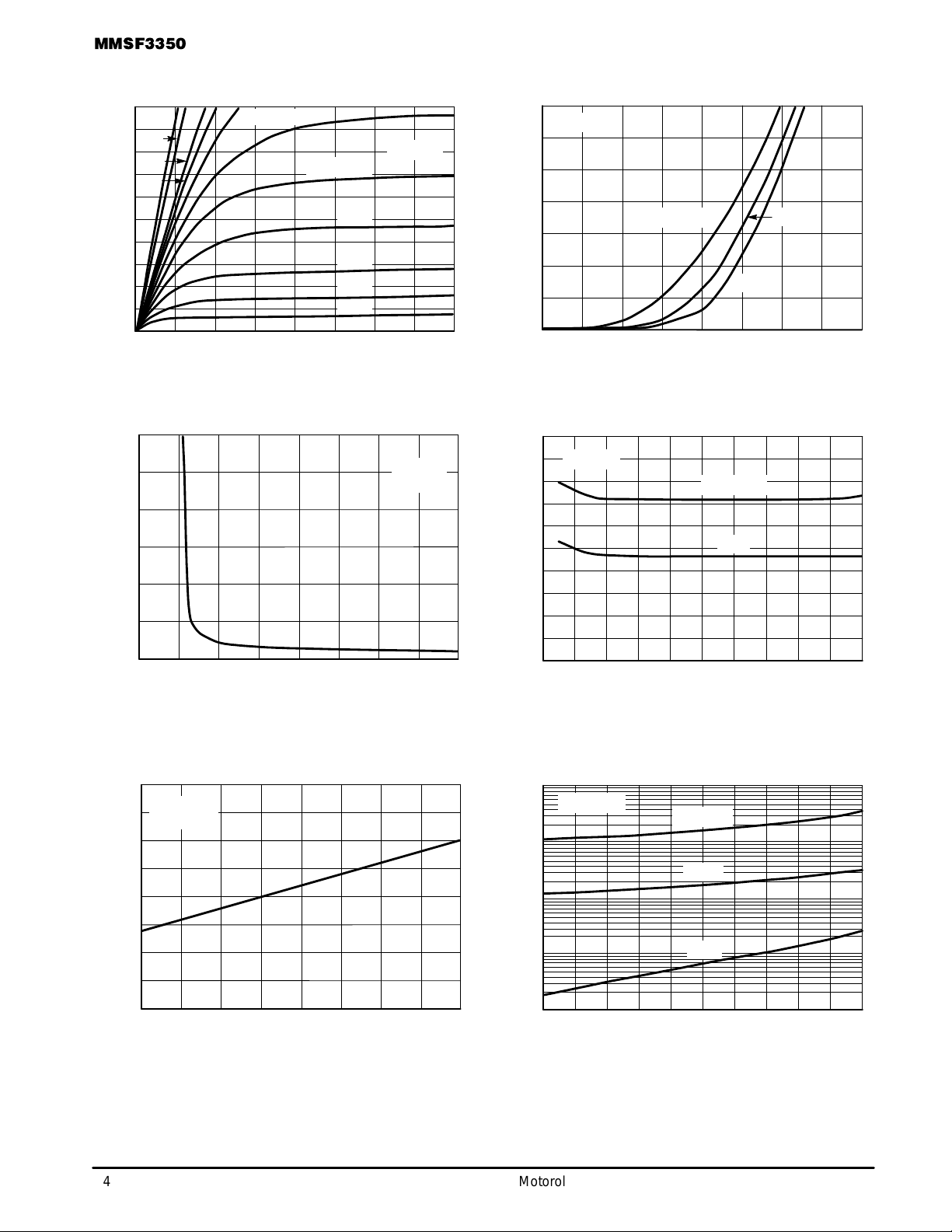
TYPICAL ELECTRICAL CHARACTERISTICS
25
10 V
6.0 V
20
4.5 V
4.3 V
15
10
, DRAIN CURRENT (AMPS)
D
I
5
0
0 0.25 0.5 1.251.0
VDS, DRAIN–TO–SOURCE VOL TAGE (VOLTS)
Figure 1. On–Region Characteristics
0.3
0.2
0.1
, DRAIN–TO–SOURCE RESIST ANCE (OHMS)
0
DS(on)
R
324 10
VGS, GATE–T O–SOURCE VOLTAGE (VOLTS)
4.1 V 3.9 V
TJ = 25°C
VGS = 3.7 V
3.5 V
3.3 V
3.1 V
2.9 V
0.75
579
68
1.5 2.0
1.75
ID = 5.0 A
TJ = 25
°
C
14
VDS ≥ 10 V
12
10
8
6
, DRAIN CURRENT (AMPS)
4
D
I
2
0
24
2.5
VGS, GATE–T O–SOURCE VOLTAGE (VOLTS)
TJ = 125°C
3 3.5
25°C
–55°C
Figure 2. Transfer Characteristics
0.020
0.018
0.016
0.014
0.012
0.010
0.008
0.006
0.004
, DRAIN–TO–SOURCE RESIST ANCE (OHMS)
0.002
DS(on)
R
TJ = 25°C
VGS = 4.5 V
10 V
0
0 5 10 25
ID, DRAIN CURRENT (AMPS)
15
20
Figure 3. On–Resistance versus
Gate–T o–Source Voltage
2.0
VGS = 10 V
ID = 10 A
1.5
1.0
(NORMALIZED)
0.5
, DRAIN–TO–SOURCE RESIST ANCE
DS(on)
R
0
–50 –25 0 25 50 75 100 125 150
°
TJ, JUNCTION TEMPERATURE (
C)
Figure 5. On–Resistance Variation with
T emperature
Figure 4. On–Resistance versus Drain Current
and Gate Voltage
1000
VGS = 0 V
100
10
, LEAKAGE (nA)
DSS
I
1
0.1
51015 30
VDS, DRAIN–TO–SOURCE VOL TAGE (VOLTS)
TJ = 125°C
100°C
25°C
20 25
Figure 6. Drain–T o–Source Leakage
Current versus Voltage
4
Motorola TMOS Power MOSFET Transistor Device Data
 Loading...