

Motorola MMSF3205R2 Datasheet
1
Motorola TMOS Power MOSFET Transistor Device Data
Medium Power Surface Mount Products
MiniMOS devices are an advanced series of power MOSFETs
which utilize Motorola’s High Cell Density HDTMOS process. These
miniature surface mount MOSFETs feature ultra low R
DS(on)
and true
logic level performance. They are capable of withstanding high energy in
the avalanche and commutation modes and the drain–to–s ource diode
has a very low reverse recovery time. MiniMOS devices are designed for
use in low voltage, high speed switching applications where power
efficiency is important. Typical applications are dc–dc converters, and
power management in portable and battery powered products such as
computers, printers, cellular and cordless phones. They can also be
used for low voltage motor controls in mass storage products such as
disk drives and tape drives. The avalanche energy is specified to
eliminate the guesswork in des igns where induc tive loads are switched
and offer additional safety margin against unexpected voltage transients.
• Ultra Low R
DS(on)
Provides Higher Efficiency and Extends Battery Life
• Logic Level Gate Drive — Can Be Driven by Logic ICs
• Miniature SO–8 Surface Mount Package — Saves Board Space
• Diode Is Characterized for Use In Bridge Circuits
• Diode Exhibits High Speed, With Soft Recovery
• I
DSS
Specified at Elevated Temperature
• Avalanche Energy Specified
• Mounting Information for SO–8 Package Provided
DEVICE MARKING ORDERING INFORMATION
Device Reel Size Tape Width Quantity
S3205
MMSF3205R2 13″ 12 mm embossed tape 4000 units
HDTMOS and MiniMOS are trademarks of Motorola, Inc. TMOS is a registered trademark of Motorola, Inc.
Preferred devices are Motorola recommended choices for future use and best overall value.
This document contains information on a product under development. Motorola reserves the right to change or discontinue this product without notice.
Order this document
by MMSF3205/D
SEMICONDUCTOR TECHNICAL DATA
Motorola, Inc. 1998
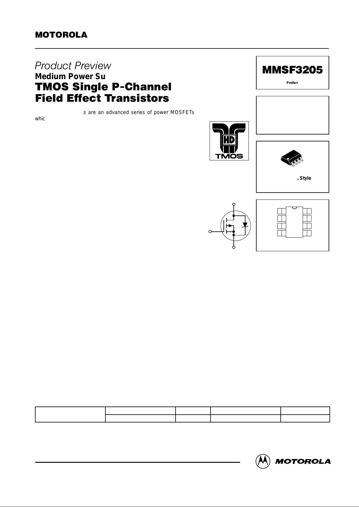
CASE 751–06, Style 12
SO–8
SINGLE TMOS
POWER MOSFET
11 AMPERES
20 VOLTS
R
DS(on)
= 0.015 OHM
Motorola Preferred Device
Source
1
2
3
4
8
7
6
5
Top View
Source
Source
Gate
Drain
Drain
Drain
Drain
D
S
G
MMSF3205
2
Motorola TMOS Power MOSFET Transistor Device Data
MAXIMUM RATINGS
(TJ = 25°C unless otherwise noted)
Negative sign for P–Channel devices omitted for clarity
Rating
Symbol Max Unit
Drain–to–Source Voltage V
DSS
20 V
Drain–to–Gate Voltage (RGS = 1.0 MΩ) V
DGR
20 V
Gate–to–Source Voltage — Continuous V
GS
± 12 V
1 inch SQ.
FR–4 or G–10 PCB
10 seconds
Thermal Resistance — Junction to Ambient
Total Power Dissipation @ TA = 25°C
Linear Derating Factor
Drain Current — Continuous @ TA = 25°C
Continuous @ TA = 70°C
Pulsed Drain Current
(1)
R
THJA
P
D
I
D
I
D
I
DM
50
2.5
20
11
8.0
55
°C/W
Watts
mW/°C
A
A
A
Minimum
FR–4 or G–10 PCB
10 seconds
Thermal Resistance — Junction to Ambient
Total Power Dissipation @ TA = 25°C
Linear Derating Factor
Drain Current — Continuous @ TA = 25°C
Continuous @ TA = 70°C
Pulsed Drain Current
(1)
R
THJA
P
D
I
D
I
D
I
DM
80
1.56
12.5
8.6
6.4
43
°C/W
Watts
mW/°C
A
A
A
Operating and Storage Temperature Range TJ, T
stg
– 55 to 150 °C
Single Pulse Drain–to–Source Avalanche Energy — Starting TJ = 25°C
(VDD = 20 Vdc, VGS = 4.5 Vdc, Peak IL = 11 Apk, L = TBD mH, RG = 25 W)
E
AS
TBD
mJ
(1) Repetitive rating; pulse width limited by maximum junction temperature.
 Loading...