

1
Motorola TMOS Power MOSFET Transistor Device Data
Medium Power Surface Mount Products
MiniMOS devices are an advanced series of power MOSFETs
which utilize Motorola’s TMOS process. These miniature surface
mount MOSFETs feature ultra low R
DS(on)
and true logic level
performance. They are capable of withstanding high energy in the
avalanche and commutation modes and the drain–to–source diode
has a low reverse recovery time. MiniMOS devices are designed
for use in low voltage, high speed switching applications where
power efficiency is important. Typical applications are dc–dc
converters, a nd power m anagement in portable a nd battery
powered products such as computers, printers, cellular and
cordless phones. They can also be used for low voltage motor
controls in mass storage products such as disk drives and tape
drives. The a valanche energy i s specified to e liminate the
guesswork in designs where inductive loads are switched and offer
additional safety margin against unexpected voltage transients.
• Ultra Low R
DS(on)
Provides Higher Efficiency and Extends Battery Life
• Logic Level Gate Drive — Can Be Driven by Logic ICs
• Miniature SO–8 Surface Mount Package — Saves Board Space
• Diode Is Characterized for Use In Bridge Circuits
• Diode Exhibits High Speed
• Avalanche Energy Specified
• Mounting Information for SO–8 Package Provided
• I
DSS
Specified at Elevated Temperature
MAXIMUM RATINGS
(TJ = 25°C unless otherwise noted)
(1)
Rating
Symbol Value Unit
Drain–to–Source Voltage V
DSS
20 Vdc
Gate–to–Source Voltage — Continuous V
GS
± 20 Vdc
Drain Current — Continuous @ TA = 25°C
(2)
Drain Current — Continuous @ TA = 100°C
Drain Current — Single Pulse (tp ≤ 10 µs)
I
D
I
D
I
DM
2.5
1.7
13
Adc
Apk
Total Power Dissipation @ TA = 25°C
(2)
P
D
2.5 Watts
Operating and Storage Temperature Range TJ, T
stg
– 55 to 150 °C
Single Pulse Drain–to–Source Avalanche Energy — Starting TJ = 25°C
(VDD = 20 Vdc, VGS = 5.0 Vdc, IL = 6.0 Apk, L = 12 mH, RG = 25 Ω)
E
AS
216 mJ
Thermal Resistance — Junction to Ambient
(2)
R
θJA
50 °C/W
Maximum Lead Temperature for Soldering Purposes, 1/8″ from case for 10 seconds T
L
260 °C
DEVICE MARKING
S2P02
(1) Negative sign for P–Channel device omitted for clarity .
(2) Mounted on 2” square FR4 board (1” sq. 2 oz. Cu 0.06” thick single sided), 10 sec. max.
ORDERING INFORMATION
Device Reel Size Tape Width Quantity
MMSF2P02ER2 13″ 12 mm embossed tape 2500 units
Designer’s Data for “Worst Case” Conditions — The Designer’s Data Sheet permits the design of most circuits entirely from the information presented. SOA Limit
curves — representing boundaries on device characteristics — are given to facilitate “worst case” design.
Designer’s, HDTMOS and MiniMOS are trademarks of Motorola, Inc. TMOS is a registered trademark of Motorola, Inc.
Thermal Clad is a registered trademark of Bergquist Company.
Preferred
devices are Motorola recommended choices for future use and best overall value.
REV 4
Order this document
by MMSF2P02E/D
SEMICONDUCTOR TECHNICAL DATA
Motorola, Inc. 1996
CASE 751–05, Style 13
SO–8
N–C
1
2
3
4
8
7
6
5
Top View
Source
Source
Gate
Drain
Drain
Drain
Drain
D
S
G
SINGLE TMOS
POWER MOSFET
2.5 AMPERES
20 VOLTS
R
DS(on)
= 0.250 OHM
Motorola Preferred Device
查询MMSF2P02E供应商
MMSF2P02E
2
Motorola TMOS Power MOSFET Transistor Device Data
ELECTRICAL CHARACTERISTICS
(TA = 25°C unless otherwise noted)
(1)
Characteristic
Symbol Min Typ Max Unit
OFF CHARACTERISTICS
Drain–to–Source Breakdown Voltage
(VGS = 0 Vdc, ID = 250 µAdc)
Temperature Coefficient (Positive)
V
(BR)DSS
20
—
—
24.7
—
—
Vdc
mV/°C
Zero Gate Voltage Drain Current
(VDS = 20 Vdc, VGS = 0 Vdc)
(VDS = 20 Vdc, VGS = 0 Vdc, TJ = 125°C)
I
DSS
—
—
—
—
1.0
10
µAdc
Gate–Body Leakage Current (VGS = ± 20 Vdc, VDS = 0) I
GSS
— — 100 nAdc
ON CHARACTERISTICS
(2)
Gate Threshold Voltage
(VDS = VGS, ID = 250 µAdc)
Threshold Temperature Coefficient (Negative)
V
GS(th)
1.0 2.0
4.7
3.0
—
Vdc
mV/°C
Static Drain–to–Source On–Resistance
(VGS = 10 Vdc, ID = 2.0 Adc)
(VGS = 4.5 Vdc, ID = 1.0 Adc)
R
DS(on)
—
—
0.19
0.3
0.25
0.4
Ohm
Forward Transconductance (VDS = 3.0 Vdc, ID = 1.0 Adc) g
FS
1.0 2.8 — Mhos
DYNAMIC CHARACTERISTICS
Input Capacitance
C
iss
— 340 475 pF
Output Capacitance
(VDS = 16 Vdc, VGS = 0 Vdc,
f = 1.0 MHz)
C
oss
— 220 300
Transfer Capacitance
f = 1.0 MHz)
C
rss
— 75 150
SWITCHING CHARACTERISTICS
(3)
Turn–On Delay Time
t
d(on)
— 20 40 ns
Rise Time
t
r
— 40 80
Turn–Off Delay Time
VGS = 5.0 Vdc,
RG = 6.0 Ω)
t
d(off)
— 53 106
Fall Time
G
= 6.0 Ω)
t
f
— 41 82
Turn–On Delay Time
t
d(on)
— 13 26 ns
Rise Time
t
r
— 29 58
Turn–Off Delay Time
VGS = 10 Vdc,
RG = 6.0 Ω)
t
d(off)
— 30 60
Fall Time
G
= 6.0 Ω)
t
f
— 28 56
Q
T
— 10 15
DS
= 16 Vdc, ID = 2.0 Adc,
Q
1
— 1.1 —
(VDS = 16 Vdc, ID = 2.0 Adc,
VGS = 10 Vdc)
Q
2
— 3.3 —
Q
3
— 2.5 —
SOURCE–DRAIN DIODE CHARACTERISTICS
Forward On–Voltage
(2)
(IS = 2.0 Adc, VGS = 0 Vdc) V
SD
— 1.5 2.0 Vdc
t
rr
— 34 64
S
= 2.0 Adc, VGS = 0 Vdc,
t
a
— 18 —
(IS = 2.0 Adc, VGS = 0 Vdc,
dIS/dt = 100 A/µs)
t
b
— 16 —
Reverse Recovery Stored Charge Q
RR
— 0.035 — µC
(1) Negative sign for P–Channel device omitted for clarity.
(2) Pulse Test: Pulse Width ≤ 300 µs, Duty Cycle ≤ 2%.
(3) Switching characteristics are independent of operating junction temperature.
Gate Charge
Reverse Recovery Time
(VDD = 10 Vdc, ID = 2.0 Adc,
(VDD = 10 Vdc, ID = 2.0 Adc,
(V
(I
nC
ns
MMSF2P02E
3
Motorola TMOS Power MOSFET Transistor Device Data
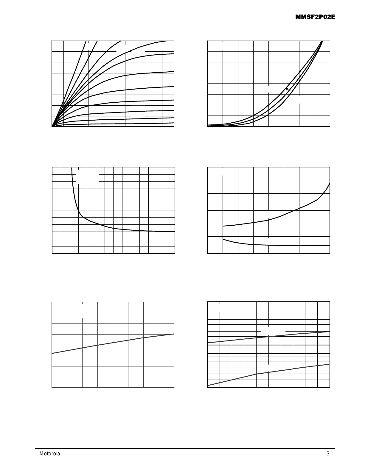
TYPICAL ELECTRICAL CHARACTERISTICS
3.5 V
10 V
R
DS(on)
, DRAIN–TO–SOURCE RESISTANCE (NORMALIZED)
R
DS(on)
, DRAIN–TO–SOURCE RESISTANCE (OHMS)
R
DS(on)
, DRAIN–TO–SOURCE RESISTANCE (OHMS)
0
0 0.4 0.8 1.2 1.6 2
0
2
3
VDS, DRAIN–TO–SOURCE VOLTAGE (VOLTS)
Figure 1. On–Region Characteristics
I
D
, DRAIN CURRENT (AMPS)
I
D
, DRAIN CURRENT (AMPS)
VGS, GATE–TO–SOURCE VOLTAGE (VOLTS)
Figure 2. Transfer Characteristics
3 4 5 10
0.3
0.4
0.6
0.1
VGS, GATE–TO–SOURCE VOLTAGE (VOLTS)
Figure 3. On–Resistance versus
Gate–to–Source Voltage
ID, DRAIN CURRENT (AMPS)
Figure 4. On–Resistance versus Drain Current
and Gate Voltage
1
TJ, JUNCTION TEMPERATURE (
°
C)
Figure 5. On–Resistance Variation with
Temperature
VDS, DRAIN–TO–SOURCE VOLTAGE (VOLTS)
Figure 6. Drain–to–Source Leakage Current
versus Voltage
0.2
6 8
–50 0 50 100 150
4
1
0
3.3 V
TJ = 25°C
VGS = 10
2
3
4
1
2.5 3 3.5 4 4.5
0.1
0.4
0.5
0.6
0.3
0.2
0 0.5 1 1.5 2
0
I
DSS
, LEAKAGE (nA)
100
10
0 4 8 12 20
0.5
1.0
1.5
2.0
VGS = 10 V
ID = 2 A
1257525–25
VDS ≥ 10 V
25°C
100°C
TJ = –55°C
VGS = 4.5
TJ = 25°C
9
7
0.5
ID = 1 A
TJ = 25
°
C
16
3.7 V
3.9 V
4.1 V
4.3 V
4.5 V
5 V
4.7 V
7 V
VGS = 0 V
TJ = 125°C
100°C
MMSF2P02E
4
Motorola TMOS Power MOSFET Transistor Device Data
POWER MOSFET SWITCHING
Switching behavior is most easily modeled and predicted
by recognizing that the power MOSFET is charge controlled.
The lengths of various switching intervals (∆t) are determined by how fast the FET input capacitance can be charged
by current from the generator.
The published capacitance data is difficult to use for calculating rise and fall because drain–gate capacitance varies
greatly with applied voltage. Accordingly , gate charge data is
used. In most cases, a satisfactory estimate of average input
current (I
G(AV)
) can be made from a rudimentary analysis of
the drive circuit so that
t = Q/I
G(AV)
During the rise and fall time interval when switching a resistive load, VGS remains virtually constant at a level known as
the plateau voltage, V
SGP
. Therefore, rise and fall times may
be approximated by the following:
tr = Q2 x RG/(VGG – V
GSP
)
tf = Q2 x RG/V
GSP
where
VGG = the gate drive voltage, which varies from zero to V
GG
RG = the gate drive resistance
and Q2 and V
GSP
are read from the gate charge curve.
During the turn–on and turn–off delay times, gate current is
not constant. The simplest calculation uses appropriate values from the capacitance curves in a standard equation for
voltage change in an RC network. The equations are:
t
d(on)
= RG C
iss
In [VGG/(VGG – V
GSP
)]
t
d(off)
= RG C
iss
In (VGG/V
GSP
)
The capacitance (C
iss
) is read from the capacitance curve at
a voltage corresponding to the off–state condition when calculating t
d(on)
and is read at a voltage corresponding to the
on–state when calculating t
d(off)
.
At high switching speeds, parasitic circuit elements complicate the analysis. The inductance of the MOSFET source
lead, inside the package and in the circuit wiring which is
common to both the drain and gate current paths, produces a
voltage at the source which reduces the gate drive current.
The voltage is determined by Ldi/dt, but since di/dt is a function of drain current, the mathematical solution is complex.
The M OSFET output capacitance also complicates the
mathematics. And finally, MOSFETs have finite internal gate
resistance which effectively adds to the resistance of the
driving source, but the internal resistance is difficult to measure and, consequently, is not specified.
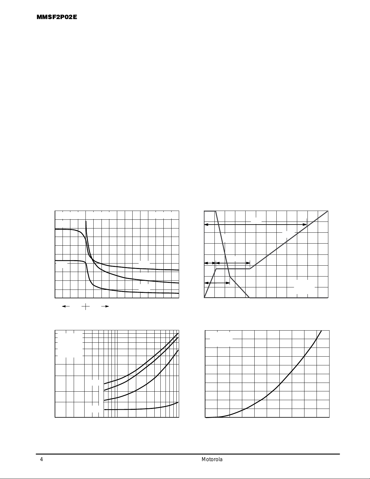
C, CAPACITANCE (pF)
GATE–TO–SOURCE OR DRAIN–TO–SOURCE VOLTAGE (VOLTS)
Figure 7. Capacitance Variation
V
GS
, GATE–TO–SOURCE VOLTAGE (VOLTS)
Qg, TOTAL GATE CHARGE (nC)
Figure 8. Gate–to–Source and
Drain–to–Source Voltage versus Total Charge
t, TIME (ns)
RG, GATE RESISTANCE (OHMS)
100
Figure 9. Resistive Switching Time Variation
versus Gate Resistance
1 10010
10
I
S
, SOURCE CURRENT (AMPS)
VSD, SOURCE–TO–DRAIN VOLTAGE (VOLTS)
0.4
0.8
1.2
2
Figure 10. Diode Forward Voltage
versus Current
1.6
0.6 0.8 1.2 1.4 1.61
0
TJ = 25°C
VGS = 0 V
0 2 4 6 8
ID = 2 A
TJ = 25
°
C
V
GS
6
3
0
12
9
16
12
8
4
0
V
DS
QT
Q1
Q2
Q3
10 12
10 0 10 15 25
V
GS
V
DS
TJ = 25
°C
VDS = 0 V VGS = 0 V
1000
800
600
400
200
0
20
C
iss
C
oss
C
rss
5 5
C
iss
C
rss
30
V
DS
, DRAIN–TO–SOURCE VOLTAGE (VOLTS)
VDD = 10 V
ID = 2 A
VGS = 10 V
TJ = 25
°
C
t
f
t
d(off)
t
d(on)
t
r

MMSF2P02E
5
Motorola TMOS Power MOSFET Transistor Device Data
Figure 11. Reverse Recovery Time (trr)
TJ, STARTING JUNCTION TEMPERATURE (°C)
E
AS
, SINGLE PULSE DRAIN–TO–SOURCE
Figure 12. Maximum Rated Forward Biased
Safe Operating Area
AVALANCHE ENERGY (mJ)
0
25 50 75 100 125
150
ID = 6 A
200
150
250
100
50
I
S
, SOURCE CURRENT
t, TIME
Figure 13. Maximum Avalanche Energy versus
Starting Junction Temperature
di/dt = 300 A/µs
Standard Cell Density
High Cell Density
t
b
t
rr
t
a
t
rr
0.1
VDS, DRAIN–TO–SOURCE VOLTAGE (VOLTS)
1
10
I
D
, DRAIN CURRENT (AMPS)
R
DS(on)
LIMIT
THERMAL LIMIT
PACKAGE LIMIT
0.01
VGS = 20 V
SINGLE PULSE
TC = 25°C
10
0.1
dc
10 ms
1
100
100
Mounted on 2” sq. FR4 board (1” sq. 2 oz. Cu 0.06”
thick single sided), 10s max.
1 ms
Although many E–FETs can withstand the stress of drain–
to–source avalanche at currents up to rated pulsed current
(IDM), the energy rating is specified at rated continuous current (ID), in accordance with industry custom. The energy
rating must be derated for temperature as shown in the accompanying graph (Figure 13). Maximum energy at currents
below rated continuous ID can safely be assumed to equal
the values indicated.
Figure 14. Thermal Response
t, TIME (s)
Rthja(t), EFFECTIVE TRANSIENT
THERMAL RESISTANCE
1
0.1
0.01
D = 0.5
SINGLE PULSE
1.0E–05 1.0E–04 1.0E–03 1.0E–02 1.0E–01 1.0E+00 1.0E+01
0.2
0.1
0.05
0.02
0.01
1.0E+02 1.0E+03
0.001
10
0.0022 Ω0.0210 Ω0.2587 Ω0.7023 Ω0.6863
Ω
108.44 F3.1413 F0.3517 F0.0207 F0.0020 F
Chip
Ambient
Normalized to θja at 10s.

MMSF2P02E
6
Motorola TMOS Power MOSFET Transistor Device Data
Figure 15. Diode Reverse Recovery Waveform
di/dt
t
rr
t
a
t
p
I
S
0.25 I
S
TIME
I
S
t
b
INFORMATION FOR USING THE SO–8 SURFACE MOUNT PACKAGE
MINIMUM RECOMMENDED FOOTPRINT FOR SURFACE MOUNTED APPLICATIONS
Surface mount board layout is a critical portion of the total
design. The footprint for the semiconductor packages must be
the correct size to ensure proper solder connection interface
between the board and the package. With the correct pad
geometry, the packages will self–align when subjected to a
solder reflow process.
mm
inches
0.060
1.52
0.275
7.0
0.024
0.6
0.050
1.270
0.155
4.0
SO–8 POWER DISSIPATION
The power dissipation of the SO–8 is a function of the input
pad size. This can vary from the minimum pad size for
soldering to the pad size given for maximum power
dissipation. Power dissipation for a surface mount device is
determined by T
J(max)
, the maximum rated junction
temperature of the die, R
θJA
, the thermal resistance from the
device junction to ambient; and the operating temperature, TA.
Using the values provided on the data sheet for the SO–8
package, PD can be calculated as follows:
PD =
T
J(max)
– T
A
R
θJA
The values for the equation are found in the maximum
ratings table on the data sheet. Substituting these values into
the equation for an ambient temperature TA of 25°C, one can
calculate the power dissipation of the device which in this case
is 2.5 Watts.
PD =
150°C – 25°C
50°C/W
= 2.5 Watts
The 50°C/W for the SO–8 package assumes the
recommended footprint on a glass epoxy printed circuit board
to achieve a power dissipation of 2.5 Watts using the footprint
shown. Another alternative would be to use a ceramic
substrate or an aluminum core board such as Thermal Clad.
Using board material such as Thermal Clad, the power
dissipation can be doubled using the same footprint.

MMSF2P02E
7
Motorola TMOS Power MOSFET Transistor Device Data
SOLDERING PRECAUTIONS
The melting temperature of solder is higher than the rated
temperature of the device. When the entire device is heated
to a high temperature, failure to complete soldering within a
short time could result in device failure. Therefore, the
following items should always be observed in order to
minimize the thermal stress to which the devices are
subjected.
• Always preheat the device.
• The delta temperature between the preheat and soldering
should be 100°C or less.*
• When preheating and soldering, the temperature of the
leads and the case must not exceed the maximum
temperature ratings as shown on the data sheet. When
using infrared heating with the reflow soldering method,
the difference shall be a maximum of 10°C.
• The soldering temperature and time shall not exceed
260°C for more than 10 seconds.
• When shifting from preheating to soldering, the maximum
temperature gradient shall be 5°C or less.
• After soldering has been completed, the device should be
allowed to cool naturally for at least three minutes.
Gradual cooling should be used as the use of forced
cooling will increase the temperature gradient and result
in latent failure due to mechanical stress.
• Mechanical stress or shock should not be applied during
cooling.
* Soldering a device without preheating can cause excessive
thermal shock and stress which can result in damage to the
device.
TYPICAL SOLDER HEATING PROFILE
For any given circuit board, there will be a group of control
settings that will give the desired heat pattern. The operator
must set temperatures for several heating zones and a figure
for belt speed. T aken together , these control settings make up
a heating “profile” for that particular circuit board. On
machines controlled by a computer, the computer remembers
these profiles from one operating session to the next. Figure
13 shows a typical heating profile for use when soldering a
surface mount device to a printed circuit board. This profile will
vary among soldering systems, but it is a good starting point.
Factors that can affect the profile include the type of soldering
system in use, density and types of components on the board,
type of solder used, and the type of board or substrate material
being used. This profile shows temperature versus time. The
line on the graph shows the actual temperature that might be
experienced on the surface of a test board at or near a central
solder joint. The two profiles are based on a high density and
a low density board. The Vitronics SMD310 convection/infrared reflow soldering system was used to generate this
profile. The type of solder used was 62/36/2 Tin Lead Silver
with a melting point between 177–189°C. When this type of
furnace is used for solder reflow work, the circuit boards and
solder joints tend to heat first. The components on the board
are then heated by conduction. The circuit board, because it
has a large surface area, absorbs the thermal energy more
efficiently, then distributes this energy to the components.
Because of this effect, the main body of a component may be
up to 30 degrees cooler than the adjacent solder joints.
STEP 1
PREHEAT
ZONE 1
“RAMP”
STEP 2
VENT
“SOAK”
STEP 3
HEATING
ZONES 2 & 5
“RAMP”
STEP 4
HEATING
ZONES 3 & 6
“SOAK”
STEP 5
HEATING
ZONES 4 & 7
“SPIKE”
STEP 6
VENT
STEP 7
COOLING
200
°
C
150
°
C
100
°
C
50
°
C
TIME (3 TO 7 MINUTES TOTAL)
T
MAX
SOLDER IS LIQUID FOR
40 TO 80 SECONDS
(DEPENDING ON
MASS OF ASSEMBLY)
205
°
TO 219°C
PEAK AT
SOLDER JOINT
DESIRED CURVE FOR LOW
MASS ASSEMBLIES
100°C
150°C
160
°
C
170°C
140
°
C
Figure 16. Typical Solder Heating Profile
DESIRED CURVE FOR HIGH
MASS ASSEMBLIES

MMSF2P02E
8
Motorola TMOS Power MOSFET Transistor Device Data
PACKAGE DIMENSIONS
STYLE 13:
PIN 1. N.C.
2. SOURCE
3. SOURCE
4. GATE
5. DRAIN
6. DRAIN
7. DRAIN
8. DRAIN
CASE 751–05
SO–8
ISSUE P
SEATING
PLANE
1
4
58
C
K
4X P
A0.25 (0.010)MT B
S S
0.25 (0.010)
M
B
M
8X D
R
M
J
X 45
_
_
F
–A–
–B–
–T–
DIM MIN MAX
MILLIMETERS
A 4.80 5.00
B 3.80 4.00
C 1.35 1.75
D 0.35 0.49
F 0.40 1.25
G 1.27 BSC
J 0.18 0.25
K 0.10 0.25
M 0 7
P 5.80 6.20
R 0.25 0.50
__
G
NOTES:
1. DIMENSIONS A AND B ARE DATUMS AND T IS A
DATUM SURFACE.
2. DIMENSIONING AND TOLERANCING PER ANSI
Y14.5M, 1982.
3. DIMENSIONS ARE IN MILLIMETER.
4. DIMENSION A AND B DO NOT INCLUDE MOLD
PROTRUSION.
5. MAXIMUM MOLD PROTRUSION 0.15 PER SIDE.
6. DIMENSION D DOES NOT INCLUDE MOLD
PROTRUSION. ALLOWABLE DAMBAR
PROTRUSION SHALL BE 0.127 TOTAL IN EXCESS
OF THE D DIMENSION AT MAXIMUM MATERIAL
CONDITION.
Motorola reserves the right to make changes without further notice to any products herein. Motorola makes no warranty , representation or guarantee regarding
the suitability of its products for any particular purpose, nor does Motorola assume any liability arising out of the application or use of any product or circuit, and
specifically disclaims any and all liability , including without limitation consequential or incidental damages. “Typical” parameters which may be provided in Motorola
data sheets and/or specifications can and do vary in different applications and actual performance may vary over time. All operating parameters, including “Typicals”
must be validated for each customer application by customer’s technical experts. Motorola does not convey any license under its patent rights nor the rights of
others. Motorola products are not designed, intended, or authorized for use as components in systems intended for surgical implant into the body, or other
applications intended to support or sustain life, or for any other application in which the failure of the Motorola product could create a situation where personal injury
or death may occur. Should Buyer purchase or use Motorola products for any such unintended or unauthorized application, Buyer shall indemnify and hold Motorola
and its officers, employees, subsidiaries, affiliates, and distributors harmless against all claims, costs, damages, and expenses, and reasonable attorney fees
arising out of, directly or indirectly, any claim of personal injury or death associated with such unintended or unauthorized use, even if such claim alleges that
Motorola was negligent regarding the design or manufacture of the part. Motorola and are registered trademarks of Motorola, Inc. Motorola, Inc. is an Equal
Opportunity/Affirmative Action Employer.
How to reach us:
USA/EUROPE/ Locations Not Listed: Motorola Literature Distribution; JAPAN: Nippon Motorola Ltd.; Tatsumi–SPD–JLDC, 6F Seibu–Butsuryu–Center,
P.O. Box 20912; Phoenix, Arizona 85036. 1–800–441–2447 or 602–303–5454 3–14–2 Tatsumi Koto–Ku, Tokyo 135, Japan. 03–81–3521–8315
MFAX: RMFAX0@email.sps.mot.com – TOUCHTONE 602–244–6609 ASIA/PACIFIC: Motorola Semiconductors H.K. Ltd.; 8B Tai Ping Industrial Park,
INTERNET: http://Design–NET.com 51 Ting Kok Road, Tai Po, N.T., Hong Kong. 852–26629298
MMSF2P02E/D
*MMSF2P02E/D*
◊
 Loading...