

Motorola MJE340 Datasheet
1
Motorola Bipolar Power Transistor Device Data
. . . useful for high–voltage general purpose applications.
• Suitable for Transformerless, Line–Operated Equipment
• Thermopad Construction Provides High Power Dissipation Rating for High
Reliability
MAXIMUM RATINGS
Rating
Symbol
Value
Unit
Collector–Emitter Voltage
V
CEO
300
Vdc
Emitter–Base Voltage
V
EB
3.0
Vdc
Collector Current — Continuous
I
C
500
mAdc
Total Power Dissipation @ TC = 25_C
Derate above 25_C
P
D
20
0.16
Watts
W/_C
Operating and Storage Junction
Temperature Range
TJ, T
stg
–65 to +150
_
C
THERMAL CHARACTERISTICS
Characteristic
Symbol
Max
Unit
Thermal Resistance, Junction to Case
θ
JC
6.25
_
C/W
ELECTRICAL CHARACTERISTICS (T
C
= 25_C unless otherwise noted)
Characteristic
Symbol
Min
Max
Unit
OFF CHARACTERISTICS
Collector–Emitter Sustaining Voltage
(IC = 1.0 mAdc, IB = 0)
V
CEO(sus)
300
—
Vdc
Collector Cutoff Current
(VCB = 300 Vdc, IE = 0)
I
CBO
—
100
µAdc
Emitter Cutoff Current
(VEB = 3.0 Vdc, IC = 0)
I
EBO
—
100
µAdc
ON CHARACTERISTICS
DC Current Gain
(IC = 50 mAdc, VCE = 10 Vdc)
h
FE
30
240
—
SEMICONDUCTOR TECHNICAL DATA
Order this document
by MJE340/D
Motorola, Inc. 1995
0.5 AMPERE
POWER TRANSISTOR
NPN SILICON
300 VOLTS
20 WATTS
CASE 77–08
TO–225AA TYPE
REV 7
MJE340
2
Motorola Bipolar Power Transistor Device Data
28
0
TC, CASE TEMPERATURE (
°
C)
0
20 40 80 120 160
20
12
P
D
, POWER DISSIPATION (WATTS)
MJE340
32
24
16
8.0
4.0
1.0
10
IC, COLLECTOR CURRENT (mA)
0
20 30 50 100 200 500
0.4
0.8
0.6
V, VOLTAGE (VOLTS)
0.2
300
TJ = 25°C
V
BE(sat)
@ IC/IB = 10
V
CE(sat)
@ IC/IB = 10
VBE @ VCE = 10 V
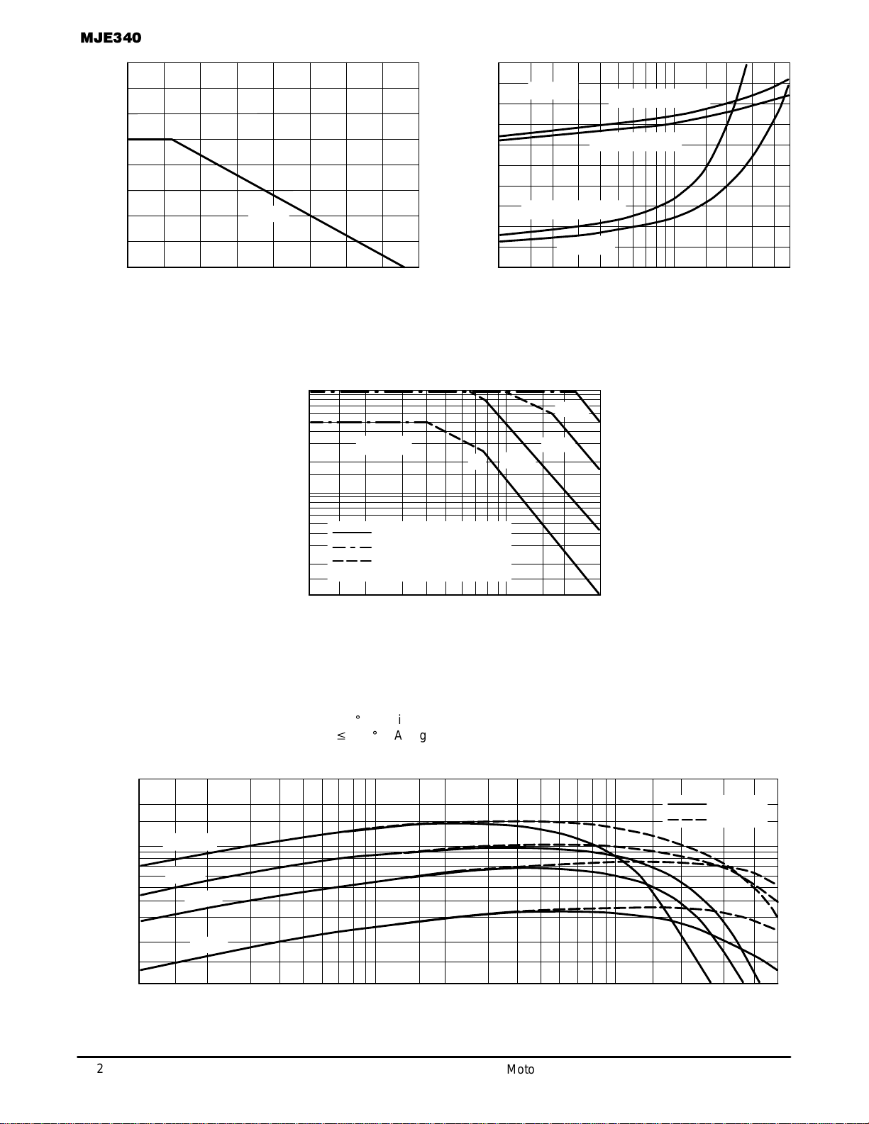
Figure 1. Power Temperature Derating
Figure 2. “On” Voltages
60 100 140
IC/IB = 5.0
Figure 3. MJE340
1.0
10
VCE, COLLECTOR–EMITTER VOLTAGE (VOLTS)
0.5
0.01
50 100
SECOND BREAKDOWN LIMIT
BONDING WIRE LIMIT
THERMAL LIMIT TC = 25°C
SINGLE PULSE
I
C
, COLLECTOR CURRENT (AMP)
dc
10 µs
0.3
0.05
20 30
1.0 ms
200 300
0.2
70
0.1
0.03
0.02
TJ = 150
°
C 500 µs
ACTIVE–REGION SAFE OPERATING AREA
There are two limitations on the power handling ability of a transistor: average junction temperature and second breakdown.
Safe operating area curves indicate IC – VCE limits of the transistor that must be observed for reliable operation; i.e., the transistor must not be subjected to greater dissipation than the curves indicate.
The data of Figure 3 is based on T
J(pk)
= 150_C; TC is variable depending on conditions. Second breakdown pulse limits are
valid for duty cycles to 10% provided T
J(pk)
v 150_C. At high case temperatures, thermal limitations will reduce the power that
can be handled to values less than the limitations imposed by second breakdown.
IC, COLLECTOR CURRENT (mAdc)
h
FE
, DC CURRENT GAIN
TJ = 150°C
+25°C
VCE = 10 V
VCE = 2.0 V
–55°C
Figure 4. DC Current Gain
300
10
200
100
1.0 2.0 3.0 5.0 10 20 30 500
70
50
7.0 50 70 100 200 300
+100°C
30
20
 Loading...