

Motorola MJE18004D2 Datasheet
1
Motorola Bipolar Power Transistor Device Data
! ' ! !% !'&#(
&,( (%)!)*&( ,!*
%*(* &##*&($!**(
!& % +!#*!% !!%*
%*!)*+(*!&% *,&("
The MJE18004D2 is state–of–art High Speed High gain BIPolar transistor (H2BIP).
High dynamic characteristics and lot to lot minimum spread (±150 ns on storage time)
make it ideally suitable for light ballast applications. Therefore, there is no need to
guarantee an hFE window.
Main features:
• Low Base Drive Requirement
• High Peak DC Current Gain (55 Typical) @ IC = 100 mA
• Extremely Low Storage Time Min/Max Guarantees Due to the
H2BIP Structure which Minimizes the Spread
• Integrated Collector–Emitter Free Wheeling Diode
• Fully Characterized and Guaranteed Dynamic V
CE(sat)
• “6 Sigma” Process Providing Tight and Reproductible Parameter Spreads
It’s characteristics make it also suitable for PFC application.
MAXIMUM RATINGS
Rating
Symbol
ОООООООО
ОООООООО
ОООООООО
Value
ÎÎÎÎ
ÎÎÎÎ
ÎÎÎÎ
Unit
Collector–Emitter Sustaining Voltage
V
CEO
ОООООООО
ОООООООО
ОООООООО
450
ÎÎÎÎ
ÎÎÎÎ
ÎÎÎÎ
Vdc
Collector–Base Breakdown Voltage
V
CBO
ОООООООО
ОООООООО
ОООООООО
1000
ÎÎÎÎ
ÎÎÎÎ
ÎÎÎÎ
Vdc
Collector–Emitter Breakdown Voltage
V
CES
ОООООООО
ОООООООО
ОООООООО
1000
ÎÎÎÎ
ÎÎÎÎ
ÎÎÎÎ
Vdc
Emitter–Base Voltage
V
EBO
ОООООООО
ОООООООО
ОООООООО
12
ÎÎÎÎ
ÎÎÎÎ
ÎÎÎÎ
Vdc
Collector Current — Continuous
Collector Current — Peak (1)
I
C
I
CM
ОООООООО
ОООООООО
ОООООООО
ОООООООО
5
10
ÎÎÎÎ
ÎÎÎÎ
ÎÎÎÎ
ÎÎÎÎ
Adc
Base Current — Continuous
Base Current — Peak (1)
I
B
I
BM
ОООООООО
ОООООООО
ОООООООО
2
4
ÎÎÎÎ
ÎÎÎÎ
ÎÎÎÎ
Adc
*Total Device Dissipation @ TC = 25_C
*Derate above 25°C
P
D
ОООООООО
ОООООООО
ОООООООО
ОООООООО
75
0.6
ÎÎÎÎ
ÎÎÎÎ
ÎÎÎÎ
ÎÎÎÎ
Watt
W/_C
Operating and Storage Temperature
TJ, T
stg
ОООООООО
ОООООООО
ОООООООО
–65 to 150
ÎÎÎÎ
ÎÎÎÎ
ÎÎÎÎ
_
C
THERMAL CHARACTERISTICS
Thermal Resistance — Junction to Case
Thermal Resistance — Junction to Ambient
R
θJC
R
θJA
ОООООООО
ОООООООО
ОООООООО
ОООООООО
1.65
62.5
ÎÎÎÎ
ÎÎÎÎ
ÎÎÎÎ
ÎÎÎÎ
_
C/W
Maximum Lead Temperature for Soldering Purposes:
1/8″ from case for 5 seconds
T
L
ОООООООО
ОООООООО
ОООООООО
260
ÎÎÎÎ
ÎÎÎÎ
ÎÎÎÎ
_
C
(1) Pulse Test: Pulse Width = 5 ms, Duty Cycle ≤ 10%.
Designer’s Data for “Worst Case” Conditions — The Designer’s Data Sheet permits the design of most circuits entirely from the information presented. SOA Limit
curves — representing boundaries on device characteristics — are given to facilitate “worst case” design.
Designer’s and SWITCHMODE are trademarks of Motorola, Inc.
SEMICONDUCTOR TECHNICAL DATA
Order this document
by MJE18004D2/D
Motorola, Inc. 1995
POWER TRANSISTORS
5 AMPERES
1000 VOLTS
75 WATTS
CASE 221A–06
TO–220AB
MJE18004D2
2
Motorola Bipolar Power Transistor Device Data
ELECTRICAL CHARACTERISTICS
(T
C
= 25°C unless otherwise noted)
Characteristic
Symbol
Min
Typ
Max
Unit
OFF CHARACTERISTICS
Collector–Emitter Sustaining Voltage
(IC = 100 mA, L = 25 mH)
V
CEO(sus)
450
547
Vdc
Collector–Base Breakdown Voltage
(I
CBO
= 1 mA)
V
CBO
1000
1100
Vdc
Emitter–Base Breakdown Voltage
(I
EBO
= 1 mA)
V
EBO
12
14
Vdc
Collector Cutoff Current
(VCE = Rated V
CEO
, IB = 0)
I
CEO
100
µAdc
Collector Cutoff Current (VCE = Rated V
CES
, VEB = 0)
Collector Cutoff Current (VCE = 500 V, VEB = 0)
@ TC = 25°C
@ TC = 125°C
@ TC = 125°C
I
CES
100
500
100
µAdc
Emitter–Cutoff Current
(VEB = 10 Vdc, IC = 0)
I
EBO
100
µAdc
ON CHARACTERISTICS
Base–Emitter Saturation Voltage
(IC = 0.8 Adc, IB = 80 mAdc)
@ TC = 25°C
@ TC = 125°C
0.8
0.7
1
0.9
(IC = 2 Adc, IB = 0.4 Adc)
@ TC = 25°C
@ TC = 125°C
0.9
0.8
1
0.9
Collector–Emitter Saturation Voltage
(IC = 0.8 Adc, IB = 80 mAdc)
@ TC = 25°C
@ TC = 125°C
0.38
0.55
0.5
0.75
(IC = 2 Adc, IB = 0.4 Adc)
@ TC = 25°C
@ TC = 125°C
0.45
0.75
0.75
1
(IC = 0.8 Adc, IB = 40 mAdc)
@ TC = 25°C
@ TC = 125°C
0.9
1.6
1.5
(IC = 1 Adc, IB = 0.2 Adc)
@ TC = 25°C
@ TC = 125°C
0.25
0.28
0.5
0.6
DC Current Gain
(IC = 0.8 Adc, VCE = 1 Vdc)
@ TC = 25°C
@ TC = 125°C
15
10
28
14
(IC = 2 Adc, VCE = 1 Vdc)
@ TC = 25°C
@ TC = 125°C
6
4
8
6
(IC = 1 Adc, VCE = 2.5 Vdc)
@ TC = 25°C
@ TC = 125°C
18
14
28
20
DYNAMIC SATURATION VOLTAGE
@ 1 µs
@ TC = 25°C
@ TC = 125°C
9
16
Dynamic Saturation
Voltage:
Determined 1 µs and
IB1 = 100 mA
VCC = 300 V
@ 3 µs
@ TC = 25°C
@ TC = 125°C
3.1
9
µs and
3 µs respectively after
rising IB1 reaches
@ 1 µs
@ TC = 25°C
@ TC = 125°C
11
18
90% of final I
B1
IB1 = 0.4 A
VCC = 300 V
@ 3 µs
@ TC = 25°C
@ TC = 125°C
1.4
8
V
BE(sat)
Vdc
IC = 1 Adc
IC = 2 Adc
V
CE(sat)
h
FE
V
CE(dsat)
Vdc
—
V
MJE18004D2
3
Motorola Bipolar Power Transistor Device Data
ELECTRICAL CHARACTERISTICS (T
C
= 25°C unless otherwise noted)
Characteristic
Symbol
Min
ÎÎÎ
ÎÎÎ
ÎÎÎ
Typ
Max
Unit
DIODE CHARACTERISTICS
Forward Diode Voltage
(IEC = 1 Adc)
@ TC = 25°C
@ TC = 125°C
ÎÎÎ
ÎÎÎ
ÎÎÎ
ÎÎÎ
ÎÎÎ
0.96
0.72
1.5
(IEC = 2 Adc)
@ TC = 25°C
@ TC = 125°C
ÎÎÎ
ÎÎÎ
ÎÎÎ
1.15
0.8
1.7
Forward Recovery Time
(IF = 0.4 Adc, di/dt = 10 A/µs)
@ TC = 25°C
ÎÎÎ
ÎÎÎ
ÎÎÎ
ÎÎÎ
440
(IF = 1 Adc, di/dt = 10 A/µs)
@ TC = 25°C
ÎÎÎ
ÎÎÎ
ÎÎÎ
335
(IF = 2 Adc, di/dt = 10 A/µs)
@ TC = 25°C
ÎÎÎ
ÎÎÎ
ÎÎÎ
335
DYNAMIC CHARACTERISTICS
Current Gain Bandwidth
(IC = 0.5 Adc, VCE = 10 Vdc, f = 1 MHz)
f
T
ÎÎÎ
ÎÎÎ
ÎÎÎ
ÎÎÎ
13
MHz
Output Capacitance
(VCB = 10 Vdc, IE = 0, f = 1 MHz)
C
ob
ÎÎÎ
ÎÎÎ
ÎÎÎ
60
100
pF
Input Capacitance
(IC = 0.5 Adc, VCE = 10 Vdc, f = 1 MHz)
C
ib
ÎÎÎ
ÎÎÎ
ÎÎÎ
ÎÎÎ
450
750
pF
SWITCHING CHARACTERISTICS: Resistive Load (D.C. ≤ 10%, Pulse Width = 40 µs)
Turn–on Time
@ TC = 25°C
t
on
ÎÎÎ
ÎÎÎ
ÎÎÎ
500
750
ns
Turn–off Time
IB2 = 1 Adc
VCC = 250 Vdc
@ TC = 25°C
t
off
1.1
ÎÎÎ
ÎÎÎ
ÎÎÎ
1.4
µs
Turn–on Time
@ TC = 25°C
@ TC = 125°C
t
on
ÎÎÎ
ÎÎÎ
ÎÎÎ
ÎÎÎ
100
150
150
ns
Turn–off Time
IB2 = 1 Adc
VCC = 300 Vdc
@ TC = 25°C
@ TC = 125°C
t
off
ÎÎÎ
ÎÎÎ
ÎÎÎ
ÎÎÎ
1.15
1.6
1.3
µs
Turn–on Time
@ TC = 25°C
@ TC = 125°C
t
on
ÎÎÎ
ÎÎÎ
ÎÎÎ
120
500
150
ns
Turn–off Time
IB2 = 0.5 Adc
VCC = 300 Vdc
@ TC = 25°C
@ TC = 125°C
t
off
1.85
ÎÎÎ
ÎÎÎ
ÎÎÎ
ÎÎÎ
2.6
2.15
µs
SWITCHING CHARACTERISTICS: Inductive Load (VCC = 15 V)
Fall Time
@ TC = 25°C
@ TC = 125°C
t
f
ÎÎÎ
ÎÎÎ
ÎÎÎ
ÎÎÎ
130
300
175
ns
Storage Time
C
= 2.5 Adc
IB1 = 500 mAdc
IB2 = 500 mAdc
V
= 350 V
@ TC = 25°C
@ TC = 125°C
t
s
ÎÎÎ
ÎÎÎ
ÎÎÎ
2.12
2.6
2.4
µs
Crossover Time
VZ = 350 V
LC = 300 µH
@ TC = 25°C
@ TC = 125°C
t
c
ÎÎÎ
ÎÎÎ
ÎÎÎ
ÎÎÎ
355
750
500
ns
Fall Time
@ TC = 25°C
@ TC = 125°C
t
f
ÎÎÎ
ÎÎÎ
ÎÎÎ
ÎÎÎ
95
230
150
ns
Storage Time
C
= 2 Adc
IB1 = 400 mAdc
IB2 = 400 mAdc
V
= 300 V
@ TC = 25°C
@ TC = 125°C
t
s
2.1
ÎÎÎ
ÎÎÎ
ÎÎÎ
2.9
2.4
µs
Crossover Time
VZ = 300 V
LC = 200 µH
@ TC = 25°C
@ TC = 125°C
t
c
ÎÎÎ
ÎÎÎ
ÎÎÎ
ÎÎÎ
300
700
450
ns
Fall Time
@ TC = 25°C
@ TC = 125°C
t
f
ÎÎÎ
ÎÎÎ
ÎÎÎ
ÎÎÎ
70
100
90
ns
Storage Time
C
= 1 Adc
IB1 = 100 mAdc
IB2 = 500 mAdc
V
= 300 V
@ TC = 25°C
@ TC = 125°C
t
s
ÎÎÎ
ÎÎÎ
ÎÎÎ
0.7
1.05
0.9
µs
Crossover Time
VZ = 300 V
LC = 200 µH
@ TC = 25°C
@ TC = 125°C
t
c
ÎÎÎ
ÎÎÎ
ÎÎÎ
ÎÎÎ
75
160
120
ns
V
EC
t
fr
IC = 2.5 Adc, IB1 = 0.5 Adc
IC = 2 Adc, IB1 = 0.4 Adc
IC = 2.5 Adc, IB1 = 0.5 Adc
IC = 2.5 Adc
IC = 2 Adc
IC = 1 Adc
V
ns
MJE18004D2
4
Motorola Bipolar Power Transistor Device Data
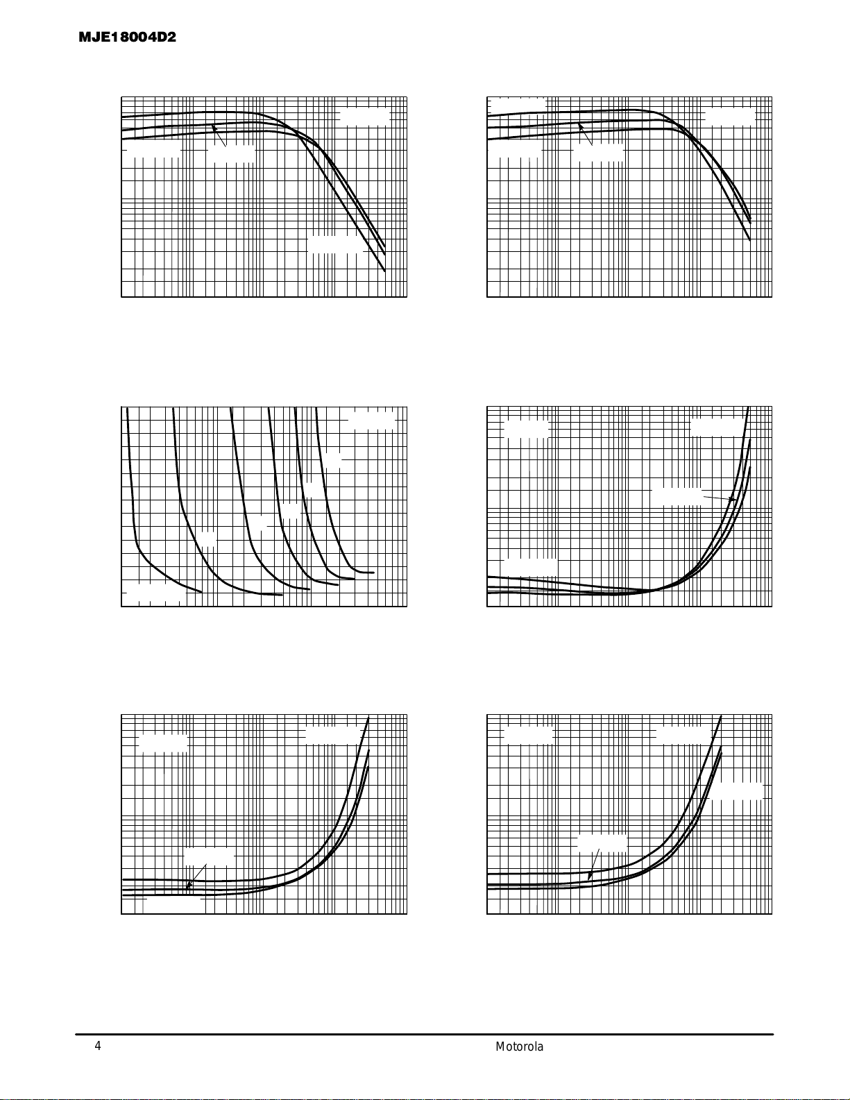
TYPICAL STATIC CHARACTERISTICS
Figure 1. DC Current Gain @ 1 Volt
100
10
1
1010.10.010.001
IC, COLLECTOR CURRENT (AMPS)
h
FE
, DC CURRENT GAIN
TJ = 125°C
TJ = 25°C
TJ = –20°C
VCE = 1 V
Figure 2. DC Current Gain @ 5 Volt
100
10
1
1010.10.010.001
IC, COLLECTOR CURRENT (AMPS)
h
FE
, DC CURRENT GAIN
TJ = 125°C
TJ = –20°C
VCE = 5 V
Figure 3. Collector Saturation Region
3
2
0
1010.10.01
IB, BASE CURRENT (mA)
IC = 500 mA
Figure 4. Collector–Emitter Saturation Voltage
10
1
0.1
1010.10.010.001
IC, COLLECTOR CURRENT (AMPS)
TJ = 125
°
C
TJ = 25°C
TJ = –20°C
IC/IB = 5
V
CE
, VOLTAGE (VOLTS)
V
CE
, VOLTAGE (VOLTS)
1
TJ = 25°C
1 A
5 A
Figure 5. Collector–Emitter Saturation Voltage
10
1
0.1
100.10.010.001
IC, COLLECTOR CURRENT (AMPS)
Figure 6. Collector–Emitter Saturation Voltage
10
1
0.1
100.10.010.001
IC, COLLECTOR CURRENT (AMPS)
TJ = 125
°
C
TJ = –20°C
V
CE
, VOLTAGE (VOLTS)
V
CE
, VOLTAGE (VOLTS)
1
IC/IB = 10
TJ = 125°C
TJ = –20°C
IC/IB = 20
4 A
3 A
2 A
TJ = 25°C
TJ = 25°C
TJ = 25°C
1
 Loading...