

Motorola MJE1320 Datasheet
1
Motorola Bipolar Power Transistor Device Data
Switchmode Series
This transistor is designed for high–voltage, power switching in inductive circuits
where RBSOA and breakdown voltage are critical. They are particularly suited for
line–operated switchmode applications.
Typical Applications:
• Fluorescent Lamp Ballasts
• Inverters
• Solenoid and Relay Drivers
• Motor Controls
• Deflection Circuits
Features:
• High V
CEV
Capability (1800 Volts)
• Low Saturation Voltage
• 100_C Performance Specified for:
Reverse–Biased SOA with Inductive Loads
Switching Times with Inductive Loads
Saturation Voltages
Leakage Currents
MAXIMUM RATINGS
Rating
Symbol
ОООООООО
ОООООООО
ОООООООО
Value
ÎÎÎÎ
ÎÎÎÎ
ÎÎÎÎ
Unit
Collector–Emitter Voltage
V
CEO(sus)
ОООООООО
ОООООООО
ОООООООО
900
ÎÎÎÎ
ÎÎÎÎ
ÎÎÎÎ
Vdc
Collector–Emitter Voltage
V
CEV
ОООООООО
ОООООООО
ОООООООО
1800
ÎÎÎÎ
ÎÎÎÎ
ÎÎÎÎ
Vdc
Emitter Base Voltage
V
EB
ОООООООО
ОООООООО
ОООООООО
9
ÎÎÎÎ
ÎÎÎÎ
ÎÎÎÎ
Vdc
Collector Current — Continuous
Peak(1)
I
C
I
CM
ОООООООО
ОООООООО
ОООООООО
2
5
ÎÎÎÎ
ÎÎÎÎ
ÎÎÎÎ
Adc
Base Current — Continuous
Peak(1)
I
B
I
BM
ОООООООО
ОООООООО
ОООООООО
ОООООООО
1.5
2.5
ÎÎÎÎ
ÎÎÎÎ
ÎÎÎÎ
ÎÎÎÎ
Adc
Total Power Dissipation @ TC = 25_C
@ TC = 100_C
Derate above 25_C
P
D
ОООООООО
ОООООООО
ОООООООО
ОООООООО
80
32
0.64
ÎÎÎÎ
ÎÎÎÎ
ÎÎÎÎ
ÎÎÎÎ
Watts
W/_C
Operating and Storage Junction Temperature Range
TJ, T
stg
ОООООООО
ОООООООО
ОООООООО
–65 to +150
ÎÎÎÎ
ÎÎÎÎ
ÎÎÎÎ
_
C
THERMAL CHARACTERISTICS
Characteristic
Symbol
ОООООООО
ОООООООО
ОООООООО
Max
ÎÎÎÎ
ÎÎÎÎ
ÎÎÎÎ
Unit
Thermal Resistance, Junction to Case
R
θJC
ОООООООО
ОООООООО
ОООООООО
1.56
ÎÎÎÎ
ÎÎÎÎ
ÎÎÎÎ
_
C/W
Maximum Lead Temperature for Soldering
Purposes: 1/8″ from Case for 5 Seconds
T
L
ОООООООО
ОООООООО
ОООООООО
275
ÎÎÎÎ
ÎÎÎÎ
ÎÎÎÎ
_
C
(1) Pulse Test: Pulse Width = 5 ms, Duty Cycle v 10%.
Designer’s Data for “Worst Case” Conditions — The Designer’s Data Sheet permits the design of most circuits entirely from the information presented. SOA Limit
curves — representing boundaries on device characteristics — are given to facilitate “worst case” design.
SWITCHMODE is a trademark of Motorola, Inc.
SEMICONDUCTOR TECHNICAL DATA
Order this document
by MJE1320/D
Motorola, Inc. 1995
POWER TRANSISTOR
2 AMPERES
900 VOLTS
80 WATTS
CASE 221A–06
TO–220AB
MJE1320
2
Motorola Bipolar Power Transistor Device Data
ELECTRICAL CHARACTERISTICS (T
C
= 25_C unless otherwise noted)
Characteristic
Symbol
Min
Typ
Max
ÎÎÎ
ÎÎÎ
ÎÎÎ
Unit
OFF CHARACTERISTICS
Collector–Emitter Sustaining Voltage
(IC = 50 mA, IB = 0)
V
CEO(sus)
900
—
—
ÎÎÎ
ÎÎÎ
ÎÎÎ
ÎÎÎ
Vdc
Collector Cutoff Current
(V
CEV
= Rated Value, V
BE(off)
= 1.5 Vdc)
(V
CEV
= Rated Value, V
BE(off)
= 1.5 Vdc, TC = 100_C)
I
CEV
—
—
—
—
0.25
2.5
ÎÎÎ
ÎÎÎ
ÎÎÎ
ÎÎÎ
mAdc
Emitter Cutoff Current
(VEB = 9 Vdc, IC = 0)
I
EBO
—
—
0.25
ÎÎÎ
ÎÎÎ
ÎÎÎ
ÎÎÎ
mAdc
SECOND BREAKDOWN
Second Breakdown Collector Current with base forward biased
I
S/b
See Figure 13
Clamped Inductive SOA with Base Reverse Biased
RBSOA
See Figure 14
ON CHARACTERISTICS
(1)
DC Current Gain (VCE = 5 Vdc) IC = 2 Adc
IC = 1 Adc
h
FE
2.5
3
4.5
7
—
—
ÎÎÎ
ÎÎÎ
ÎÎÎ
—
—
Collector–Emitter Saturation Voltage
(IC = 1 Adc, IB = 0.5 Adc)
(IC = 2 Adc, IB = 1 Adc)
(IC = 1 Adc, IB = 0.5 Adc, TC = 100_C)
V
CE(sat)
—
—
—
0.18
0.3
0.3
1
2.5
1.5
ÎÎÎ
ÎÎÎ
ÎÎÎ
ÎÎÎ
ÎÎÎ
Vdc
Base–Emitter Saturation Voltage
(IC = 1 Adc, IB = 0.5 Adc)
(IC = 2 Adc, IB = 1 Adc)
(IC = 1 Adc, IB = 0.5 Adc, TC = 100_C)
V
BE(sat)
—
—
—
0.2
0.9
0.15
1.5
2.8
1.5
ÎÎÎ
ÎÎÎ
ÎÎÎ
ÎÎÎ
ÎÎÎ
Vdc
DYNAMIC CHARACTERISTICS
Output Capacitance
(VCB = 10 Vdc, IE = 0, f
test
= 1 MHz)
C
ob
—
80
—
ÎÎÎ
ÎÎÎ
ÎÎÎ
ÎÎÎ
pF
SWITCHING CHARACTERISTICS
Resistive Load (Table 1)
Delay Time
t
d
—
0.1
—
ÎÎÎ
ÎÎÎ
ÎÎÎ
µs
Rise Time
t
r
—
0.8
—
ÎÎÎ
ÎÎÎ
ÎÎÎ
µs
Storage Time
IB1 = IB2 = 0.5 Adc
tp = 25 µs, Duty Cycle v 2%
t
s
—
4
—
ÎÎÎ
ÎÎÎ
ÎÎÎ
µs
Fall Time
p
= 25 µs, Duty Cycle v 2%
t
f
—
0.8
—
ÎÎÎ
ÎÎÎ
ÎÎÎ
µs
Inductive Load, Clamped (Table 2)
Storage Time
t
sv
—
2.8
—
ÎÎÎ
ÎÎÎ
ÎÎÎ
µs
Crossover Time
TC = 25_C
t
c
—
2.2
—
ÎÎÎ
ÎÎÎ
ÎÎÎ
µs
Storage Time
IC = 1 A, V
clamp
= 400 Vdc,
V
= 2 Vdc, I
= 0.5 Adc
t
sv
—
3.7
10.5
ÎÎÎ
ÎÎÎ
ÎÎÎ
µs
Crossover Time
V
BE(off)
= 2 Vdc, IB1 = 0.5 Adc
_
C
t
c
—
3.5
10
ÎÎÎ
ÎÎÎ
ÎÎÎ
µs
Fall Time
_
C
ÎÎÎ
ÎÎÎ
ÎÎÎ
(1) Pulse Test: Pulse Width = 300 µs. Duty Cycle v 2%.
VCC = 250 Vdc, IC = 1 A
TC = 100
MJE1320
3
Motorola Bipolar Power Transistor Device Data
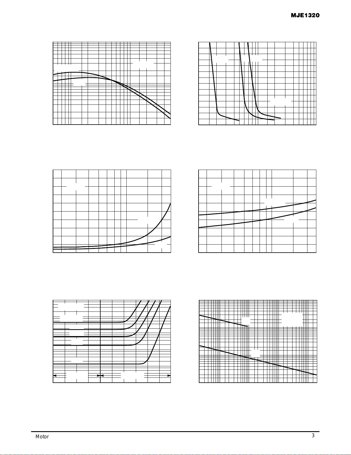
C, CAPACITANCE (pF)
V
CE
, COLLECTOR–EMITTER VOLTAGE (VOLTS)V
BE
, BASE–EMITTER VOLTAGE (VOLTS)
V
CE
, COLLECTOR–EMITTER VOLTAGE (VOLTS)
0.05
IC, COLLECTOR CURRENT (AMPS)
0.2 0.5 3
5
2
100
h
FE
, DC CURRENT GAIN
VCE = 5 V
TC = 100°C
20
0.3 1
25°C
3
0.1
0.7 2 5
Figure 1. DC Current Gain
70
50
30
10
7
1
2.5 A
Figure 2. Collector Saturation Region
IB, BASE CURRENT (AMP)
1.2
0.4
0
0.1
2
0.8
TJ = 25°C
1.6
IC = 1 A
2 A
105210.70.50.30.2
IC, COLLECTOR CURRENT (AMPS)
1.3
0.9
2
IC, COLLECTOR CURRENT (AMPS)
1.6
1.2
0.4
0
0.3
Figure 3. Collector–Emitter Saturation Voltage
0.25 0.3 0.4 2.51 1.50.5
Figure 4. Base–Emitter Saturation Voltage
IC/IB = 2
1.1
0.7
0.7
0.5
TJ = 100°C
0.8
2
Figure 5. Collector Cutoff Region
10K
VBE, BASE–EMITTER VOLTAGE (VOLTS)
0.1
0–0.4
Figure 6. Capacitance Variation
10K
VR, REVERSE VOLTAGE (VOLTS)
C
ib
0.2
, COLLECTOR CURRENT ( A)
µ
I
C
1K
100
10
1
–0.2 +0.2 +0.4 +0.6
75°C
REVERSE FORWARD
25°C
VCE = 250 V
5K
2K
1K
500
200
100
50
20
10
0.3 0.5 1 2 5 10 20 50 100 500 2K
300
3K
30
200
0.07
2.4
2.8
7
100°C
0.25 0.3 0.4 2.51 1.50.5 0.7 2
30
3
1K
f = 1 MHz
TJ = 25
°
C
25°C
TJ = 25°C
IC/IB = 2
TJ = 150°C
125°C
100°C
C
ob
TYPICAL STATIC CHARACTERISTICS
 Loading...