

Motorola MJD47, MJD50 Datasheet

1
Motorola Bipolar Power Transistor Device Data
DPAK For Surface Mount Applications
Designed for line operated audio output amplifier, switchmode power supply drivers
and other switching applications.
• Lead Formed for Surface Mount Applications in Plastic Sleeves (No Suffix)
• Straight Lead Version in Plastic Sleeves (“–1” Suffix)
• Lead Formed Version in 16 mm Tape and Reel (“T4” Suffix)
• Electrically Similar to Popular TIP47, and TIP50
• 250 and 400 V (Min) — V
CEO(sus)
• 1 A Rated Collector Current
MAXIMUM RATINGS
Rating
Symbol
MJD47
MJD50
Unit
Collector–Emitter Voltage
V
CEO
250
400
Vdc
Collector–Base Voltage
V
CB
350
500
Vdc
Emitter–Base Voltage
V
EB
5
Vdc
Collector Current — Continuous
Peak
I
C
1
2
Adc
Base Current
I
B
0.6
Adc
Total Power Dissipation @ TC = 25_C
Derate above 25_C
P
D
15
0.12
Watts
W/_C
Total Power Dissipation* @ TA = 25_C
Derate above 25_C
P
D
1.56
0.0125
Watts
W/_C
Operating and Storage Junction
Temperature Range
TJ, T
stg
–65 to +150
_
C
THERMAL CHARACTERISTICS
Characteristic
Symbol
Max
Unit
Thermal Resistance, Junction to Case
R
θJC
8.33
_
C/W
Thermal Resistance, Junction to Ambient*
R
θJA
80
_
C/W
Lead Temperature for Soldering Purpose
T
L
260
_
C
ELECTRICAL CHARACTERISTICS (T
C
= 25_C unless otherwise noted)
Characteristic
Symbol
Min
Max
Unit
OFF CHARACTERISTICS
Collector–Emitter Sustaining Voltage (1) MJD47
(IC = 30 mAdc, IB = 0) MJD50
V
CEO(sus)
250
400
—
—
Vdc
Collector Cutoff Current
(VCE = 150 Vdc, IB = 0) MJD47
(VCE = 300 Vdc, IB = 0) MJD50
I
CEO
—
—
0.2
0.2
mAdc
*When surface mounted on minimum pad sizes recommended. (continued)
(1) Pulse Test: Pulse Width v 300 µs, Duty Cycle v 2%.
Preferred devices are Motorola recommended choices for future use and best overall value.
SEMICONDUCTOR TECHNICAL DATA
Order this document
by MJD47/D
Motorola, Inc. 1995
NPN SILICON
POWER TRANSISTORS
1 AMPERE
250, 400 VOLTS
15 WATTS
*Motorola Preferred Device
MINIMUM PAD SIZES
RECOMMENDED FOR
SURFACE MOUNTED
APPLICATIONS
0.243
6.172
0.063
1.6
0.118
3.0
0.07
1.8
0.165
4.191
0.190
4.826
inches
mm
CASE 369A–13
CASE 369–07
REV 1
2
Motorola Bipolar Power Transistor Device Data
ELECTRICAL CHARACTERISTICS – continued (T
C
= 25_C unless otherwise noted)
Characteristic
ÎÎÎÎ
ÎÎÎÎ
ÎÎÎÎ
Symbol
Min
Max
ÎÎÎ
ÎÎÎ
ÎÎÎ
Unit
OFF CHARACTERISTICS — continued
Collector Cutoff Current
(VCE = 350 Vdc, VBE = 0) MJD47
(VCE = 500 Vdc, VBE = 0) MJD50
ÎÎÎÎ
ÎÎÎÎ
ÎÎÎÎ
ÎÎÎÎ
ÎÎÎÎ
I
CES
—
—
0.1
0.1
ÎÎÎ
ÎÎÎ
ÎÎÎ
ÎÎÎ
ÎÎÎ
mAdc
Emitter Cutoff Current
(VBE = 5 Vdc, IC = 0)
ÎÎÎÎ
ÎÎÎÎ
ÎÎÎÎ
ÎÎÎÎ
I
EBO
—
1
ÎÎÎ
ÎÎÎ
ÎÎÎ
ÎÎÎ
mAdc
ON CHARACTERISTICS (1)
DC Current Gain
(IC = 0.3 Adc, VCE = 10 Vdc)
(IC = 1 Adc, VCE = 10 Vdc)
ÎÎÎÎ
ÎÎÎÎ
ÎÎÎÎ
ÎÎÎÎ
h
FE
30
10
150
—
ÎÎÎ
ÎÎÎ
ÎÎÎ
ÎÎÎ
—
Collector–Emitter Saturation Voltage
(IC = 1 Adc, IB = 0.2 Adc)
ÎÎÎÎ
ÎÎÎÎ
ÎÎÎÎ
ÎÎÎÎ
V
CE(sat)
—
1
ÎÎÎ
ÎÎÎ
ÎÎÎ
ÎÎÎ
Vdc
Base–Emitter On Voltage
(IC = 1 Adc, VCE = 10 Vdc)
ÎÎÎÎ
ÎÎÎÎ
ÎÎÎÎ
ÎÎÎÎ
V
BE(on)
—
1.5
ÎÎÎ
ÎÎÎ
ÎÎÎ
ÎÎÎ
Vdc
DYNAMIC CHARACTERISTICS
Current Gain — Bandwidth Product
(IC = 0.2 Adc, VCE = 10 Vdc, f = 2 MHz)
ÎÎÎÎ
ÎÎÎÎ
ÎÎÎÎ
ÎÎÎÎ
f
T
10
—
ÎÎÎ
ÎÎÎ
ÎÎÎ
ÎÎÎ
MHz
Small–Signal Current Gain
(IC = 0.2 Adc, VCE = 10 Vdc, f = 1 kHz)
ÎÎÎÎ
ÎÎÎÎ
ÎÎÎÎ
ÎÎÎÎ
h
fe
25
—
ÎÎÎ
ÎÎÎ
ÎÎÎ
ÎÎÎ
—
(1) Pulse Test: Pulse Width v 300 µs, Duty Cycle v 2%.
25
25
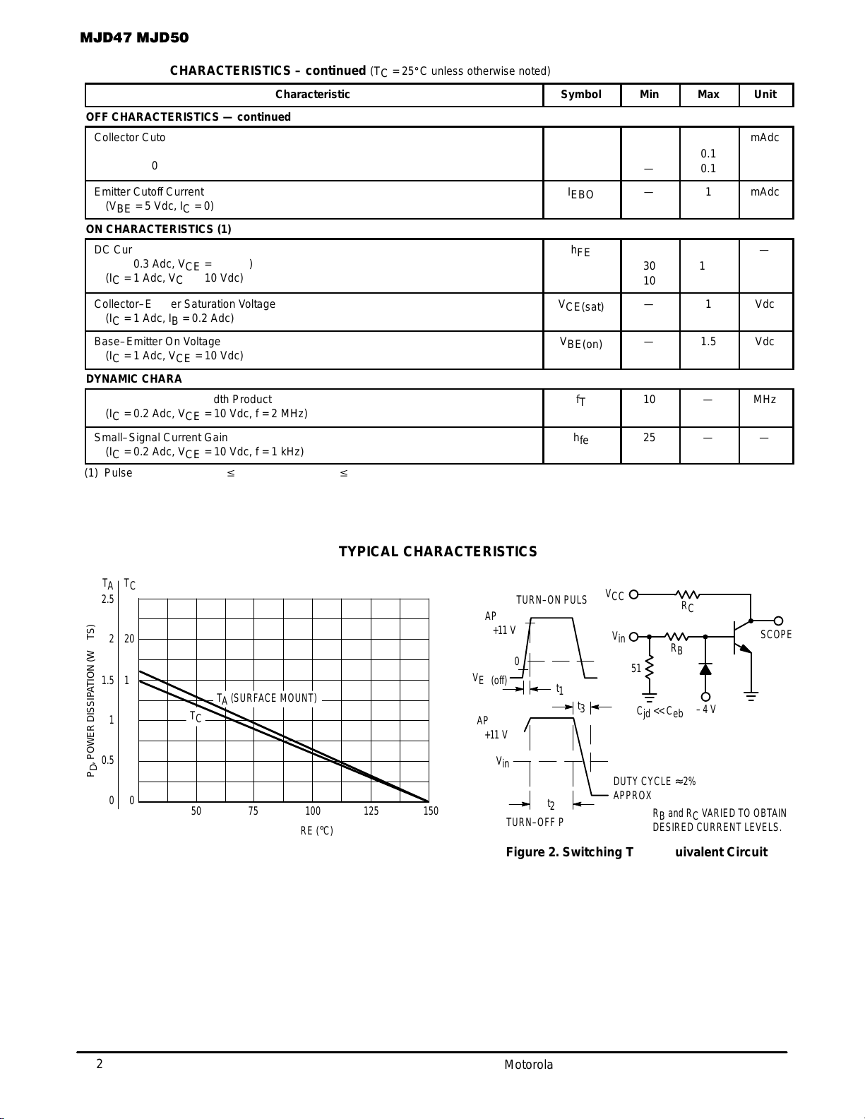
Figure 1. Power Derating
T, TEMPERATURE (°C)
0
50 75 100 125 150
20
15
10
5
P
D
, POWER DISSIPATION (WATTS)
Figure 2. Switching Time Equivalent Circuit
APPROX
+11 V
R
B
–4 V
t
1
SCOPE
V
CC
R
C
51
RB and RC VARIED TO OBTAIN
DESIRED CURRENT LEVELS.
2.5
0
2
1.5
1
0.5
TAT
C
T
C
DUTY CYCLE
≈
2%
APPROX –9 V
t1
≤
7 ns
10 < t2 < 500
µ
s
t3 < 15 ns
Vin 0
Cjd << C
eb
V
in
t
2
t
3
APPROX
+11 V
V
in
TURN–ON PULSE
TA (SURFACE MOUNT)
V
EB(off)
TURN–OFF PULSE
TYPICAL CHARACTERISTICS
 Loading...