

Motorola MJ4502 Datasheet
1
Motorola Bipolar Power Transistor Device Data
. . . for use as an output device in complementary audio amplifiers to 100–Watts
music power per channel.
• High DC Current Gain — hFE = 25–100 @ IC = 7.5 A
• Excellent Safe Operating Area
• Complement to the NPN MJ802
MAXIMUM RATINGS
Rating
Symbol
ОООООООО
ОООООООО
ОООООООО
Value
ÎÎÎÎ
ÎÎÎÎ
ÎÎÎÎ
Unit
Collector–Emitter Voltage
V
CER
ОООООООО
ОООООООО
ОООООООО
100
ÎÎÎÎ
ÎÎÎÎ
ÎÎÎÎ
Vdc
Collector–Base Voltage
V
CB
ОООООООО
ОООООООО
ОООООООО
100
ÎÎÎÎ
ÎÎÎÎ
ÎÎÎÎ
Vdc
Collector–Emitter Voltage
V
CEO
ОООООООО
ОООООООО
ОООООООО
90
ÎÎÎÎ
ÎÎÎÎ
ÎÎÎÎ
Vdc
Emitter–Base Voltage
V
EB
ОООООООО
ОООООООО
ОООООООО
4.0
ÎÎÎÎ
ÎÎÎÎ
ÎÎÎÎ
Vdc
Collector Current
I
C
ОООООООО
ОООООООО
ОООООООО
30
ÎÎÎÎ
ÎÎÎÎ
ÎÎÎÎ
Adc
Base Current
I
B
ОООООООО
ОООООООО
ОООООООО
7.5
ÎÎÎÎ
ÎÎÎÎ
ÎÎÎÎ
Adc
Total Device Dissipation @ TC = 25_C
Derate above 25_C
P
D
ОООООООО
ОООООООО
ОООООООО
ОООООООО
200
1.14
ÎÎÎÎ
ÎÎÎÎ
ÎÎÎÎ
ÎÎÎÎ
Watts
W/_C
Operating and Storage Junction Temperature Range
TJ, T
stg
ОООООООО
ОООООООО
ОООООООО
–65 to +200
ÎÎÎÎ
ÎÎÎÎ
ÎÎÎÎ
_
C
MAXIMUM RATINGS
Characteristic
Symbol
ОООООООО
ОООООООО
ОООООООО
Max
ÎÎÎÎ
ÎÎÎÎ
ÎÎÎÎ
Unit
Thermal Resistance, Junction to Case
θ
JC
ОООООООО
ОООООООО
ОООООООО
0.875
ÎÎÎÎ
ÎÎÎÎ
ÎÎÎÎ
_
C/W
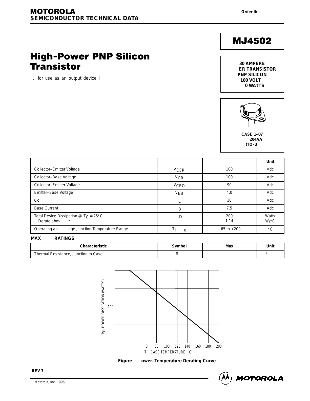
200
150
50
0
0 20 40 60 80 100 120 140 160 180 200
Figure 1. Power–Temperature Derating Curve
TC, CASE TEMPERATURE (°C)
P
D
, POWER DISSIPATION (WATTS)
100
SEMICONDUCTOR TECHNICAL DATA
Order this document
by MJ4502/D
Motorola, Inc. 1995
30 AMPERE
POWER TRANSISTOR
PNP SILICON
100 VOLTS
200 WATTS
CASE 1–07
TO–204AA
(TO–3)
REV 7
MJ4502
2
Motorola Bipolar Power Transistor Device Data
ELECTRICAL CHARACTERISTICS (T
C
= 25_C unless otherwise noted)
Characteristic
ÎÎÎÎ
ÎÎÎÎ
ÎÎÎÎ
Symbol
Min
Max
ÎÎÎ
ÎÎÎ
ÎÎÎ
Unit
OFF CHARACTERISTICS
Collector–Emitter Breakdown Voltage
(1)
(IC = 200 mAdc, RBE = 100 Ohms)
ÎÎÎÎ
ÎÎÎÎ
ÎÎÎÎ
ÎÎÎÎ
V
(BR)CER
100
—
ÎÎÎ
ÎÎÎ
ÎÎÎ
ÎÎÎ
Vdc
Collector–Emitter Sustaining Voltage
(1)
(IC = 200 mAdc)
ÎÎÎÎ
ÎÎÎÎ
ÎÎÎÎ
V
CEO(sus)
90
—
ÎÎÎ
ÎÎÎ
ÎÎÎ
Vdc
Collector–Base Cutoff Current
(VCB = 100 Vdc, IE = 0)
(VCB = 100 Vdc, IE = 0, TC = 150_C)
ÎÎÎÎ
ÎÎÎÎ
ÎÎÎÎ
ÎÎÎÎ
I
CBO
—
—
1.0
5.0
ÎÎÎ
ÎÎÎ
ÎÎÎ
ÎÎÎ
mAdc
Emitter–Base Cutoff Current (VBE = 4.0 Vdc, IC = 0)
ÎÎÎÎ
ÎÎÎÎ
ÎÎÎÎ
I
EBO
—
1.0
ÎÎÎ
ÎÎÎ
ÎÎÎ
mAdc
ON CHARACTERISTICS
DC Current Gain (IC = 7.5 Adc, VCE = 2.0 Vdc)
ÎÎÎÎ
ÎÎÎÎ
ÎÎÎÎ
h
FE
25
100
ÎÎÎ
ÎÎÎ
ÎÎÎ
—
Base–Emitter “On” Voltage (IC = 7.5 Adc, VCE = 2.0 Vdc)
ÎÎÎÎ
ÎÎÎÎ
ÎÎÎÎ
V
BE(on)
—
1.3
ÎÎÎ
ÎÎÎ
ÎÎÎ
Vdc
Collector–Emitter Saturation Voltage (IC = 7.5 Adc, IB = 0.75 Adc)
ÎÎÎÎ
ÎÎÎÎ
ÎÎÎÎ
V
CE(sat)
—
0.8
ÎÎÎ
ÎÎÎ
ÎÎÎ
Vdc
Base–Emitter Saturation Voltage (IC = 7.5 Adc, IB = 0.75 Adc)
ÎÎÎÎ
ÎÎÎÎ
ÎÎÎÎ
V
BE(sat)
—
1.3
ÎÎÎ
ÎÎÎ
ÎÎÎ
Vdc
DYNAMIC CHARACTERISTICS
Current Gain — Bandwidth Product (IC = 1.0 Adc, VCE = 10 Vdc, f = 1.0 MHz)
ÎÎÎÎ
ÎÎÎÎ
ÎÎÎÎ
f
T
2.0
—
ÎÎÎ
ÎÎÎ
ÎÎÎ
MHz
(1)
Pulse Test: Pulse Width v 300 µs, Duty Cycle v 2.0%.
3.0
0.03
Figure 2. DC Current Gain
IC, COLLECTOR CURRENT (AMP)
0.1
0.05 0.1 0.2 0.3 3.0 5.0 30
1.0
0.5
0.3
0.2
2.0
IC, COLLECTOR CURRENT (AMP)
1.4
0.8
0.6
0.4
0
TJ = 25°C
V
BE(sat)
@ IC/IB = 10
V
CE(sat)
@ IC/IB = 10
“ON” VOLTAGE (VOLTS)
Figure 3. “On” Voltages
2.0
0.7
h
FE
, NORMALIZED CURRENT GAIN
TJ = 175°C
25°C
–55°C
VCE = 2.0 V
DATA SHOWN IS OBTAINED FROM PULSE TESTS
AND ADJUSTED TO NULLIFY EFFECT OF I
CBO
.
0.5 1.0 2.0 2010
VBE @ VCE = 2.0 V
0.2
1.0
1.2
1.8
1.6
0.03 0.05 0.1 0.2 0.3 3.0 5.0 300.5 1.0 2.0 2010
Figure 4. Active Region Safe Operating Area
100
0.1
50
20
10
5.0
2.0
1.0
0.5
0.2
1.0 2.0 3.0 5.0 10 20 30 50 100
VCE, COLLECTOR-EMITTER VOLTAGE (VOLTS)
SECONDARY BREAKDOWN LIMITED
BONDING WIRE LIMITED
THERMAL LIMITATIONS @ TC = 25°C
PULSE DUTY CYCLE
v
10%
I
C
, COLLECTOR CURRENT (AMP)
TJ = 200°C
dc
5.0 ms
1.0 ms
100 µs
The Safe Operating Area Curves indicate IC – VCE limits
below which the device will not enter secondary breakdown.
Collector load lines for specific circuits must fall within the applicable Safe Area to avoid causing a catastrophic failure. To
insure operation below the maximum TJ, power–temperature
derating must be observed for both steady state and pulse
power conditions.
 Loading...