

1
Motorola Bipolar Power Transistor Device Data
. . . designed for medium–to–high voltage inverters, converters, regulators and
switching circuits.
• High Voltage — V
CEX
= 400 Vdc
• Gain Specified to 3.5 Amp
• High Frequency Response to 2.5 MHz
MAXIMUM RATINGS
Rating
Symbol
MJ413
MJ423
Unit
Collector–Emitter Voltage
V
CEX
400
400
Vdc
Collector–Base Voltage
V
CB
400
400
Vdc
Emitter–Base Voltage
V
EB
5.0
5.0
Vdc
Collector Current — Continuous
I
C
10
10
Adc
Base Current
I
B
2.0
2.0
Adc
Total Device Dissipation @ TC = 25_C
Derate above 25_C
P
D
125
1.0
Watts
W/_C
Operating Junction Temperature Range
T
J
–65 to +150
_
C
Storage Temperature Range
T
stg
–65 to +200
_
C
THERMAL CHARACTERISTICS
Characteristic
Symbol
Max
Unit
Thermal Resistance, Junction to Case
θ
JC
1.0
_
C/W
ELECTRICAL CHARACTERISTICS (T
C
= 25_C unless otherwise noted)
Characteristic
Symbol
ÎÎÎÎ
ÎÎÎÎ
ÎÎÎÎ
Min
Max
Unit
OFF CHARACTERISTICS
Collector–Emitter Sustaining Voltage* (1)
(IC = 100 mAdc, IB = 0)
V
(BR)CEO(sus)
ÎÎÎÎ
ÎÎÎÎ
ÎÎÎÎ
ÎÎÎÎ
325
—
Vdc
Collector Cutoff Current
(VCE = 400 Vdc, V
EB(off)
= 1.5 Vdc)
(VCE = 400 Vdc, V
EB(off)
= 1.5 Vdc,
T
C
= 125_C)
I
CEX
ÎÎÎÎ
ÎÎÎÎ
ÎÎÎÎ
ÎÎÎÎ
—
—
0.25
0.5
mAdc
Emitter Cutoff Current (VBE = 5.0 Vdc, IC = 0)
I
EBO
ÎÎÎÎ
ÎÎÎÎ
ÎÎÎÎ
—
5.0
mAdc
ON CHARACTERISTICS
DC Current Gain(1)
(IC = 0.5 Adc, VCE = 5.0 Vdc) MJ413
(IC = 1.0 Adc, VCE = 5.0 Vdc)
(IC = 1.0 Adc, VCE = 5.0 Vdc) MJ423
(IC = 2.5 Adc, VCE = 5.0 Vdc)
h
FE
ÎÎÎÎ
ÎÎÎÎ
ÎÎÎÎ
ÎÎÎÎ
ÎÎÎÎ
ÎÎÎÎ
20
15
30
10
80
—
90
—
—
Collector–Emitter Saturation Voltage (1)
(IC = 0.5 Adc, IB = 0.05 Adc) MJ413
(IC = 1.0 Adc, IB – 0.10 Adc) MJ423
V
CE(sat)
ÎÎÎÎ
ÎÎÎÎ
ÎÎÎÎ
ÎÎÎÎ
—
—
0.8
0.8
Vdc
Base–Emitter Saturation Voltage
(IC = 0.5 Adc, IB = 0.05 Adc) MJ413
(IC = 1.0 Adc, IB = 0.1 Adc) MJ423
V
BE(sat)
ÎÎÎÎ
ÎÎÎÎ
ÎÎÎÎ
ÎÎÎÎ
—
—
1.25
1.25
Vdc
DYNAMIC CHARACTERISTICS
Current–Gain — Bandwidth Product
(IC = 200 mAdc, VCE = 10 Vdc, f = 1.0 MHz)
f
T
ÎÎÎÎ
ÎÎÎÎ
ÎÎÎÎ
ÎÎÎÎ
2.5
—
MHz
(1) PW v 300 µs Duty Cycle v 2.0%.
SEMICONDUCTOR TECHNICAL DATA
Order this document
by MJ413/D
Motorola, Inc. 1995
10 AMPERE
POWER TRANSISTORS
NPN SILICON
400 VOLTS
125 WATTS
CASE 1–07
TO–204AA
(TO–3)
REV 7
2
Motorola Bipolar Power Transistor Device Data
I
C
, COLLECTOR CURRENT (AMPS)
I
C
, COLLECTOR CURRENT (mA) I
C
, COLLECTOR CURRENT (AMP)
100
0.1
IC, COLLECTOR CURRENT (AMP)
1.0
70
1.0
TJ = 100° C
1.0
VCE, COLLECTOR–EMITTER VOLTAGE (VOLTS)
6.0 200
1.0
0.1
100
125
TC, CASE TEMPERATURE (
°
C)
100
100
50
75
25
0
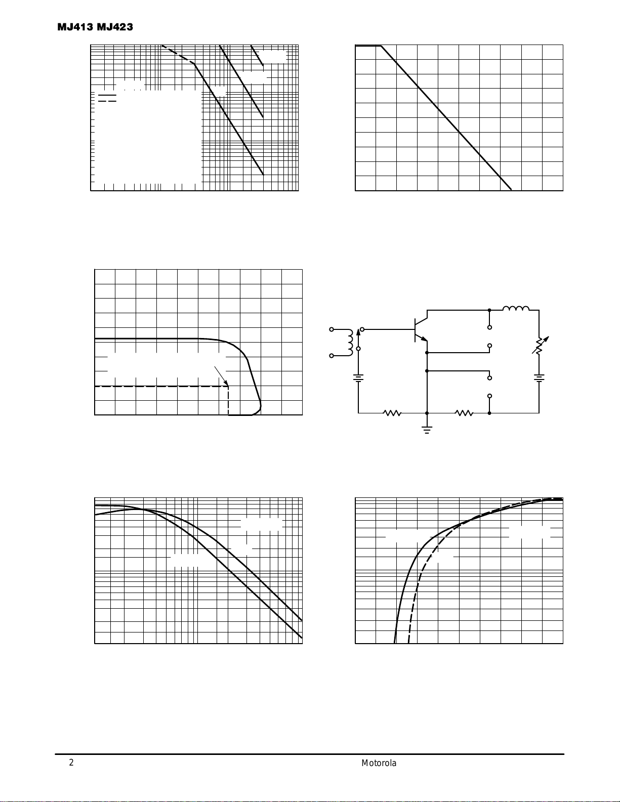
Figure 1. Active–Region Safe–Operating Area
Figure 2. Power–Temperature Derating Curve
Figure 3. Sustaining Voltage Test Load Line Figure 4. Sustaining Voltage Test Circuit
10
0.01
2.0 4.0 1000
0.2 0.3 0.5 0.7 2.0 3.0 5.0
VCE = 5.0 V
25°C
0 20 40 60 80 120 180 200
100 µs
1.0 ms
dc
0 500
V
CEO(sus)
IS ACCEPTABLE WHEN
VCE
≥
325 V AT IC = 100 mA
400
200
100
VCE, COLLECTOR–EMITTER VOLTAGE (VOLTS)
Figure 5. Current Gain
500
300
0
400300200100
200
Ω
+
–
+
–
6.0 V 50 V
TO SCOPE
X
Y
1.0
Ω
300
Ω
Hg RELAY
50 mHy
10 6020 40 400
SECONDARY BREAKDOWN LIMITATION
THERMAL LIMITATION AT T
C
= 25°C
(BASE–EMITTER DISSIPATION IS
PERCEPTIBLE ABOVE I
C
≈ 5 AMP)
The Safe Operating Area Curves indi-
cate I
C
– VCE limits below which the device will not enter secondary breakdown.
Collector load lines for specific circuits
must fall within the applicable Safe Area to
avoid causing a catastrophic failure. To insure operation below the maximum T
J
,
power temperature derating must be observed for both steady state and pulse
power conditions.
P
D
, POWER DISSIPATION (WATTS)
140 160
7.0
50
30
20
10
7.0
5.0
3.0
2.0
10
0
VBE, BASE–EMITTER VOLTAGE (VOLTS)
1.0
7.0
0.1
0.5 1.5 2.0
VCE = 10 V
Figure 6. Transconductance
2.5
5.0
3.0
2.0
1.0
0.7
0.5
0.3
0.2
h
FE
, DC CURRENT GAIN
TJ = 150°C
10
25°C
TJ = 100° C
 Loading...