

Motorola MJ410 Datasheet

1
Motorola Bipolar Power Transistor Device Data
. . . designed for medium to high voltage inverters, converters, regulators and
switching circuits.
• High Collector–Emitter Voltage —
V
CEO
= 200 Volts
• DC Current Gain Specified @ 1.0 and 2.5 Adc
• Low Collector–Emitter Saturation Voltage —
V
CE(sat)
= 0.8 Vdc @ IC = 1.0 Adc
MAXIMUM RATINGS
Rating
Symbol
Value
Unit
Collector–Emitter Voltage
V
CEO
200
Vdc
Collector–Base Voltage
V
CB
200
Vdc
Emitter–Base Voltage
V
EB
5.0
Vdc
Collector Current — Continuous
— Peak
I
C
5.0
10
Adc
Base Current
I
B
2.0
Adc
Total Device Dissipation @ TC = 75_C
Derate above 75_C
P
D
100
1.33
Watts
W/_C
Operating Junction Temperature Range
T
J
–65 to +150
_
C
Storage Temperature Range
T
stg
–65 to +200
_
C
THERMAL CHARACTERISTICS
Characteristic
Symbol
Max
Unit
Thermal Resistance, Junction to Case
θ
JC
0.75
_
C/W
ELECTRICAL CHARACTERISTICS (T
C
= 25_C unless otherwise noted)
Characteristic
Symbol
Min
Max
Unit
OFF CHARACTERISTICS
Collector–Emitter Sustaining Voltage
(IC = 100 mAdc, IB = 0)
V
CEO(sus)
200
—
Vdc
Collector Cutoff Current
(VCE = 200 Vdc, IB = 0)
I
CEO
—
0.25
mAdc
Collector Cutoff Current
(VCB = 200 Vdc, V
EB(off)
= 1.5 Vdc,
T
C
= 125_C)
I
CEX
—
0.5
mAdc
Emitter Cutoff Current (VBE = 5.0 Vdc, IC = 0)
I
EBO
—
5.0
mAdc
ON CHARACTERISTICS
DC Current Gain
(IC = 1.0 Adc, VCE = 5.0 Vdc)
(IC = 2.5 Adc, VCE = 5.0 Vdc)
h
FE
30
10
90
—
—
Collector–Emitter Saturation Voltage
(IC = 1.0 Adc, IB = 0.1 Adc)
V
CE(sat)
—
0.8
Vdc
Base–Emitter Saturation Voltage
(IC = 1.0 Adc, IB = 0.1 Adc)
V
BE(sat)
—
1.2
Vdc
DYNAMIC CHARACTERISTICS
Current–Gain — Bandwidth Product
(IC = 200 mAdc, VCE = 10 Vdc, f = 1.0 MHz)
f
T
2.5
—
MHz
SEMICONDUCTOR TECHNICAL DATA
Order this document
by MJ410/D
Motorola, Inc. 1995
5 AMPERE
POWER TRANSISTOR
NPN SILICON
200 VOLTS
100 WATTS
CASE 1–07
TO–204AA
(TO–3)
MJ410
2
Motorola Bipolar Power Transistor Device Data
I
C
, COLLECTOR CURRENT (AMP)
5.0
5.0
VCE, COLLECTOR–EMITTER VOLTAGE (VOLTS)
50 200
1.0
0.1
0.02
100
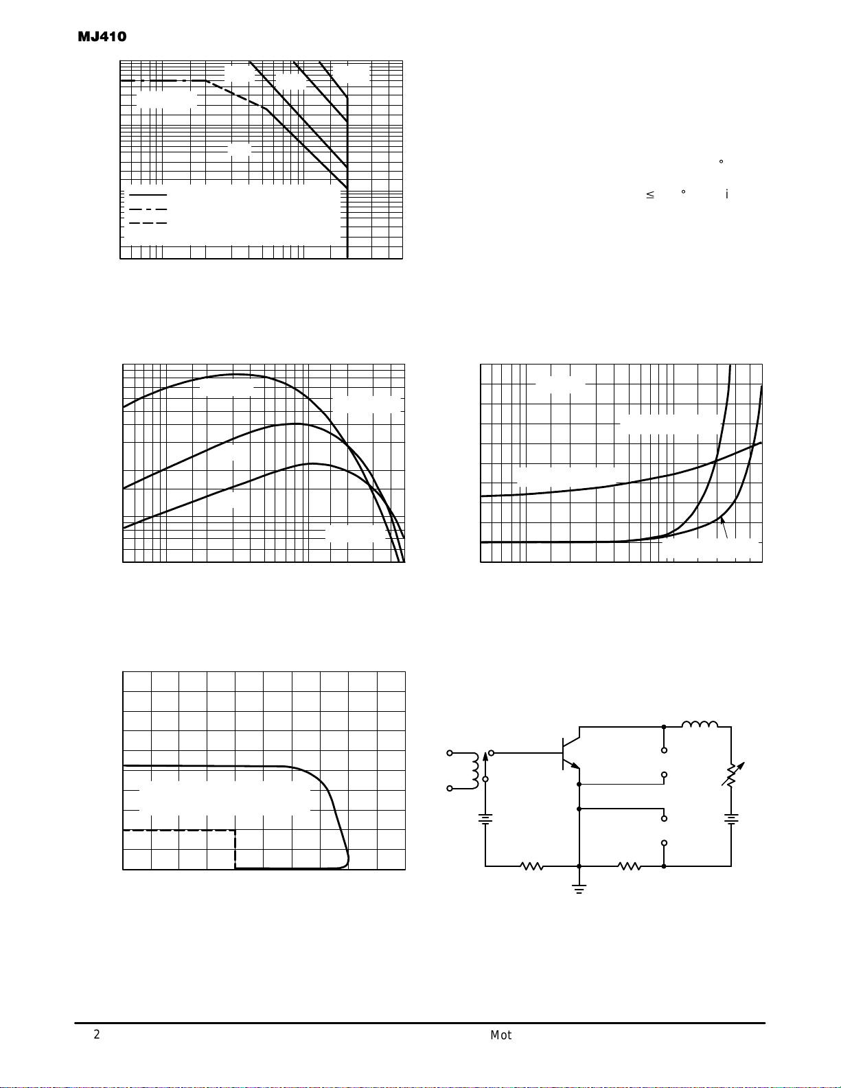
Figure 1. Active Region Safe Operating Area
10
0.5
0.2
0.05
0.01
2.0
10 20 500
TJ = 150°C
500 µs
1.0 ms
dc
SECONDARY BREAKDOWN LIMITED
BONDING WIRE LIMITED
THERMAL LIMITATION AT TC = 75
°
C
CURVES APPLY BELOW RATED V
CEO
5.0 ms
There are two limitations on the power handling ability of a
transistor: average junction temperature and second breakdown. Safe operating area curves indicate IC – VCE limits of
the transistor that must be observed for reliable operation;
i.e., the t ransistor must not be subjected to greater dissipation then the curves indicate.
The data of Figure 5 is based on T
J(pk)
= 150
_
C; TC is
variable depending on conditions. Pulse curves are valid for
duty cycles of 10% provided T
J(pk)
v 150_C. At high case
temperatures, thermal limitations will reduce the power that
can be handled to values than the limitations imposed by
second breakdown.
h
FE
, DC CURRENT GAIN
2.0
0.05
IC, COLLECTOR CURRENT (AMP)
1.0
1.6
0
1.2
0.8
0.4
TJ = 150°C
100
IC, COLLECTOR CURRENT (AMP)
1.0
70
10
30
7.0
5.0
Figure 2. DC Current Gain
Figure 3. ‘‘On” Voltages
Figure 4. Sustaining Voltage Test Load Line
0.1 0.2 0.3 0.5 2.0 3.0 5.0
V
CE(sat)
@ IC/IB = 10
V
BE(sat)
@ IC/IB = 10
VCE = 5.0 Vdc
TJ = 150°C
25°C
–55°C
TJ = 25°C
V
CE(sat)
@ IC/IB = 5
0.05 0.1 0.2 0.3 0.5 2.0 3.0 5.0
V, VOLTAGE (VOLTS)
0 500
V
CEO(sus)
IS ACCEPTABLE WHEN
VCE
≥
RATED V
CEO
AT IC = 100 mA
400
200
100
VCE, COLLECTOR–EMITTER VOLTAGE (VOLTS)
Figure 5. Sustaining Voltage Test Circuit
500
300
0
400300200100
200
Ω
+
–
+
–
6.0 V 50 V
TO SCOPE
X
Y
1.0
Ω
300
Ω
Hg RELAY
50 mH
50
20
, COLLECTOR CURRENT (mA)
C
I
 Loading...