

Motorola MJ16022, MJ16020 Datasheet
1
Motorola Bipolar Power Transistor Device Data
These transistors are designed for high–voltage, high–speed, power switching in
inductive circuits where fall time is critical. T hey a re particularly s uited f or
line–operated switchmode applications. The MJ16022 is a selected high–gain version
of the MJ16020 for applications where drive current is limited.
Features:
• Fast Switching Times:
30 ns (Typ) Inductive Fall Time
50 ns (Typ) Inductive Crossover Time
800 ns (Typ) Inductive Storage Time
• 100_C Performance Specified for:
Reverse–Biased SOA with Inductive Loads
Switching Times with Inductive Loads
Saturation Voltages
Typical Applications:
• Switching Regulators
• Inverters
• Solenoids and Relay Drivers
• Motor Controls
• Deflection Circuits
MAXIMUM RATINGS (T
C
= 25°C unless otherwise noted)
Rating
Symbol
Max
Unit
Collector–Emitter Sustaining Voltage
V
CEO
450
Vdc
Collector–Emitter Breakdown Voltage
V
CEV
850
Vdc
Emitter–Base Voltage
V
EB
6
Vdc
Collector Current — Continuous
— Peak (1)
I
C
I
CM
30
40
Adc
Base Current — Continuous
— Peak (1)
I
B
I
BM
20
30
Adc
Total Power Dissipation @ TC = 25_C
Derate above 25_C
P
D
250
1.42
Watts
W/_C
Operating and Storage Temperature
TJ, T
stg
–65 to 200
_
C
THERMAL CHARACTERISTICS
Characteristic
Symbol
Max
Unit
Thermal Resistance — Junction to Case
R
θJC
0.7
_
C/W
Maximum Lead Temperature for Soldering Purposes:
1/8″ from Case for 5 Seconds
T
L
275
_
C
(1) Pulse Test: Pulse Width = 5 ms, Duty Cycle < 10%.
This document contains information on a new product. Specifications and information herein are subject to change without notice.
SEMICONDUCTOR TECHNICAL DATA
Order this document
by MJ16020/D
Motorola, Inc. 1995
NPN SILICON POWER
TRANSISTOR
30 AMPERES
450 VOLTS
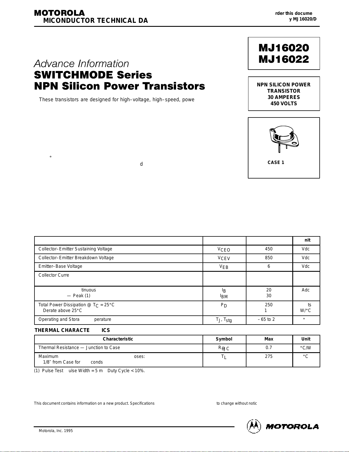
CASE 197A–05
TO–204AE
REV 7
2
Motorola Bipolar Power Transistor Device Data
ELECTRICAL CHARACTERISTICS (T
C
= 25_C unless otherwise noted)
Characteristic
Symbol
Min
Typ
Max
ÎÎÎ
ÎÎÎ
ÎÎÎ
Unit
OFF CHARACTERISTICS*
Collector–Emitter Sustaining Voltage
(IC = 1 mA, I = 0)
V
CEO(sus)
450
—
—
ÎÎÎ
ÎÎÎ
ÎÎÎ
ÎÎÎ
Vdc
Collector Cutoff Current
(VCE = 850 Vdc, RBE = 50 Ohms, TC = 100°C)
I
CER
—
—
—
ÎÎÎ
ÎÎÎ
ÎÎÎ
ÎÎÎ
mAdc
Collector Cutoff Current
(VCE = 850 Vdc, V
EB(off)
= 1.5 Vdc) @ TC = 25°C
(VCE = 850 Vdc, V
EB(off)
= 1.5 Vdc) @ TC = 100°C
I
CES
—
—
—
—
0.5
5
ÎÎÎ
ÎÎÎ
ÎÎÎ
ÎÎÎ
nAdc
Emitter Cutoff Current
(VEB = 6 Vdc, IC = 0)
I
EBO
—
—
2
ÎÎÎ
ÎÎÎ
ÎÎÎ
ÎÎÎ
nAdc
ON CHARACTERISTICS*
Base–Emitter Saturation Voltage
(IC = 20 Adc, IB = 2 Adc)
(IC = 20 Adc, IB = 2 Adc) @ TC = 100°C
V
BE(sat)
—
—
—
—
1.5
1.5
ÎÎÎ
ÎÎÎ
ÎÎÎ
ÎÎÎ
Vdc
Collector–Emitter Saturation Voltage
(IC = 20 Adc, IB = 1.4 Adc) @ TC = 25°C
(IC = 20 Adc, IB = 2.6 Adc) @ TC = 25°C
(IC = 20 Adc, IB = 2.6 Adc) @ TC = 100°C
V
CE(sat)
—
—
—
—
—
—
2.5
3
3
ÎÎÎ
ÎÎÎ
ÎÎÎ
ÎÎÎ
ÎÎÎ
Vdc
DC Current Gain
(IC = 30 Adc, VCE = 5 Vdc) MJ16020
MJ16022
h
FE
5
7
—
—
—
—
ÎÎÎ
ÎÎÎ
ÎÎÎ
ÎÎÎ
—
DYNAMIC CHARACTERISTICS
Output Capacitance
(VCB = 10 Vdc, IE = 0, f
test
= 1 MHz)
C
ob
—
—
800
ÎÎÎ
ÎÎÎ
ÎÎÎ
ÎÎÎ
pF
*Indicates Pulse Test: Pulse Width = 300 µs Max, Duty Cycle = 2%.
 Loading...