

1
Motorola Bipolar Power Transistor Device Data
The MJ15023 and MJ15025 are PowerBase power transistors designed for high
power audio, disk head positioners and other linear applications.
• High Safe Operating Area (100% Tested) —
2 A @ 80 V
• High DC Current Gain —
hFE = 15 (Min) @ IC = 8 Adc
MAXIMUM RATINGS
Rating
Symbol
MJ15023
MJ15025
Unit
Collector–Emitter Voltage
V
CEO
200
250
Vdc
Collector–Base Voltage
V
CBO
350
400
Vdc
Emitter–Base Voltage
V
EBO
5
Vdc
Collector–Emitter Voltage
V
CEX
400
Vdc
Collector Current — Continuous
Peak (1)
I
C
16
30
Adc
Base Current — Continuous
I
B
5
Adc
Total Power Dissipation @ TC = 25_C
Derate above 25_C
P
D
250
1.43
Watts
W/_C
Operating and Storage Junction
Temperature Range
TJ, T
stg
–65 to +200
_
C
THERMAL CHARACTERISTICS
Characteristic
Symbol
Max
Unit
Thermal Resistance, Junction to Case
R
θJC
0.70
_
C/W
(1) Pulse Test: Pulse Width = 5 ms, Duty Cycle v 10%.
Preferred devices are Motorola recommended choices for future use and best overall value.
SEMICONDUCTOR TECHNICAL DATA
Order this document
by MJ15023/D
Motorola, Inc. 1995
16 AMPERE
SILICON
POWER TRANSISTORS
200 AND 250 VOLTS
250 WATTS
*Motorola Preferred Device
CASE 1–07
TO–204AA
(TO–3)
REV 7
2
Motorola Bipolar Power Transistor Device Data
ELECTRICAL CHARACTERISTICS (T
C
= 25_C unless otherwise noted)
Characteristic
ÎÎÎÎ
ÎÎÎÎ
ÎÎÎÎ
Symbol
Min
Max
ÎÎÎ
ÎÎÎ
ÎÎÎ
Unit
OFF CHARACTERISTICS
Collector–Emitter Sustaining Voltage (1)
(IC = 100 mAdc, IB = 0) MJ15023
MJ15025
ÎÎÎÎ
ÎÎÎÎ
ÎÎÎÎ
ÎÎÎÎ
ÎÎÎÎ
V
CEO(sus)
200
250
—
—
ÎÎÎ
ÎÎÎ
ÎÎÎ
ÎÎÎ
ÎÎÎ
Collector Cutoff Current
(VCE = 200 Vdc, V
BE(off)
= 1.5 Vdc) MJ15023
(VCE = 250 Vdc, V
BE(off)
= 1.5 Vdc) MJ15025
ÎÎÎÎ
ÎÎÎÎ
ÎÎÎÎ
ÎÎÎÎ
I
CEX
—
—
250
250
ÎÎÎ
ÎÎÎ
ÎÎÎ
ÎÎÎ
µAdc
Collector Cutoff Current
(VCE = 150 Vdc, IB = 0) MJ15023
(VCE = 200 Vdc, IB = 0) MJ15025
ÎÎÎÎ
ÎÎÎÎ
ÎÎÎÎ
ÎÎÎÎ
ÎÎÎÎ
I
CEO
—
—
500
500
ÎÎÎ
ÎÎÎ
ÎÎÎ
ÎÎÎ
ÎÎÎ
µAdc
Emitter Cutoff Current
(VCE = 5 Vdc, IB = 0) Both
ÎÎÎÎ
ÎÎÎÎ
ÎÎÎÎ
I
EBO
—
500
ÎÎÎ
ÎÎÎ
ÎÎÎ
µAdc
SECOND BREAKDOWN
Second Breakdown Collector Current with Base Forward Biased
(VCE = 50 Vdc, t = 0.5 s (non–repetitive))
(VCE = 80 Vdc, t = 0.5 s (non–repetitive))
ÎÎÎÎ
ÎÎÎÎ
ÎÎÎÎ
ÎÎÎÎ
ÎÎÎÎ
I
S/b
5
2
—
—
ÎÎÎ
ÎÎÎ
ÎÎÎ
ÎÎÎ
ÎÎÎ
Adc
ON CHARACTERISTICS
DC Current Gain
(IC = 8 Adc, VCE = 4 Vdc)
(IC = 16 Adc, VCE = 4 Vdc)
ÎÎÎÎ
ÎÎÎÎ
ÎÎÎÎ
ÎÎÎÎ
ÎÎÎÎ
h
FE
15
5
60
—
ÎÎÎ
ÎÎÎ
ÎÎÎ
ÎÎÎ
ÎÎÎ
—
Collector–Emitter Saturation Voltage
(IC = 8 Adc, IB = 0.8 Adc)
(IC = 16 Adc, IB = 3.2 Adc)
ÎÎÎÎ
ÎÎÎÎ
ÎÎÎÎ
ÎÎÎÎ
V
CE(sat)
—
1.4
4.0
ÎÎÎ
ÎÎÎ
ÎÎÎ
ÎÎÎ
Vdc
Base–Emitter On Voltage
(IC = 8 Adc, VCE = 4 Vdc)
ÎÎÎÎ
ÎÎÎÎ
ÎÎÎÎ
ÎÎÎÎ
V
BE(on)
—
2.2
ÎÎÎ
ÎÎÎ
ÎÎÎ
ÎÎÎ
Vdc
DYNAMIC CHARACTERISTICS
Current–Gain — Bandwidth Product
(IC = 1 Adc, VCE = 10 Vdc, f
test
= 1 MHz)
ÎÎÎÎ
ÎÎÎÎ
ÎÎÎÎ
ÎÎÎÎ
f
T
4
—
ÎÎÎ
ÎÎÎ
ÎÎÎ
ÎÎÎ
MHz
Output Capacitance
(VCB = 10 Vdc, IE = 0, f
test
= 1 MHz)
ÎÎÎÎ
ÎÎÎÎ
ÎÎÎÎ
C
ob
—
600
ÎÎÎ
ÎÎÎ
ÎÎÎ
pF
(1) Pulse Test: Pulse Width = 300 µs, Duty Cycle v 2%.
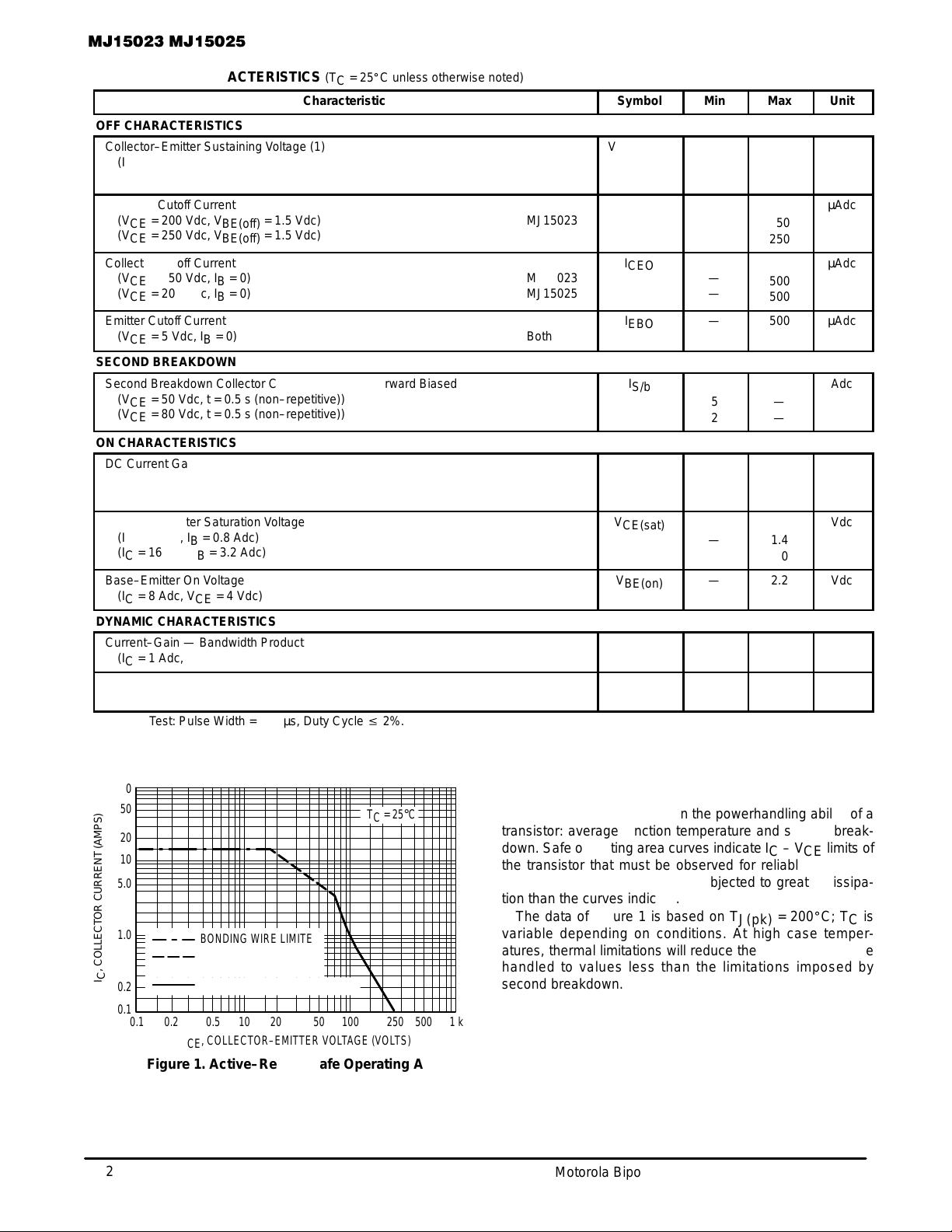
100
Figure 1. Active–Region Safe Operating Area
VCE, COLLECTOR–EMITTER VOLTAGE (VOLTS)
0.1 0.2 0.5 10 1 k
20
TC = 25°C
50 250
0.1
I
C
, COLLECTOR CURRENT (AMPS)
0.2
1.0
5.0
50
500100
10
20
BONDING WIRE LIMITED
THERMAL LIMITATION
(SINGLE PULSE)
SECOND BREAKDOWN LIMITED
There are two limitations on the powerhandling ability of a
transistor: average junction temperature and second breakdown. Safe operating area curves indicate IC – VCE limits of
the transistor that must be observed for reliable operation;
i.e., the transistor must not be subjected to greater dissipation than the curves indicate.
The data of Figure 1 is based on T
J(pk)
= 200_C; TC is
variable depending on conditions. At high case temperatures, thermal limitations will reduce the power that can be
handled to values less than the l imitations imposed b y
second breakdown.
 Loading...