

Motorola MGSF3455VT1, MGSF3455VT3 Datasheet
1
Motorola Small–Signal Transistors, FETs and Diodes Device Data
"& #
"!
! $
! !!
% #!$$%"#$
Part of the GreenLine Portfolio of devices with energy–
conserving traits.
These miniature surface mount MOSFET s utilize Motorola’s High
Cell Density, HDTMOS process. Low r
DS(on)
assures minimal
power loss and conserves energy, making this device ideal for use
in small power management circuitry. Typical applications are
dc–dc converters, power management in portable and battery–
powered products such as computers, printers, PCMCIA cards,
cellular and cordless telephones.
• Low r
DS(on)
Provides Higher Efficiency and Extends Battery Life
• Miniature TSOP 6 Surface Mount Package Saves Board Space
• Visit our Web Site at http://www.mot–sps.com/ospd
MAXIMUM RATINGS
(TJ = 25°C unless otherwise noted)
Rating Symbol Value Unit
Drain–to–Source Voltage V
DSS
30 Vdc
Gate–to–Source Voltage — Continuous V
GS
± 20 Vdc
Drain Current — Continuous @ TA = 25°C
Drain Current — Pulsed Drain Current (tp ≤ 10 µs)
I
D
I
DM
3.5
20
A
Total Power Dissipation @ TA = 25°C Mounted on FR4 t 5 sec
P
D
2.0 W
Operating and Storage Temperature Range TJ, T
stg
– 55 to 150 °C
Thermal Resistance — Junction–to–Ambient R
θJA
62.5 °C/W
Maximum Lead Temperature for Soldering Purposes, for 10 seconds T
L
260 °C
ORDERING INFORMATION
Device Reel Size Tape Width Quantity
MGSF3455VT1 7″ 8 mm embossed tape 3000
MGSF3455VT3 13″ 8 mm embossed tape 10,000
GreenLine is a trademark of Motorola, Inc.
HDTMOS is a trademark of Motorola, Inc. TMOS is a registered trademark of Motorola, Inc.
Thermal Clad is a trademark of the Bergquist Company.
This document contains information on a product under development. Motorola reserves the right to change or discontinue this product without notice.
Preferred devices are Motorola recommended choices for future use and best overall value.
Order this document
by MGSF3455VT1/D
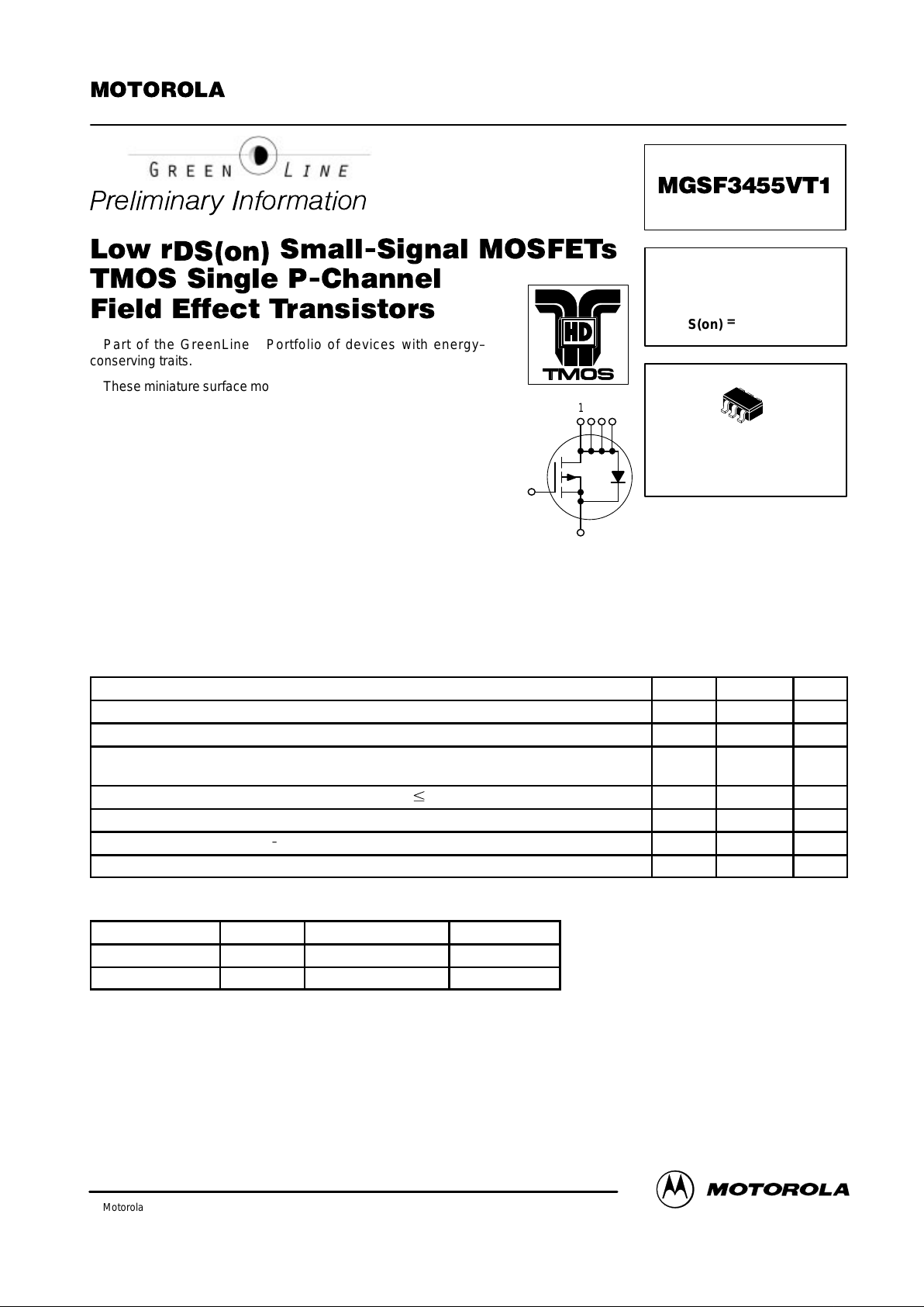
SEMICONDUCTOR TECHNICAL DATA
CASE 318G–02, Style 1
TSOP 6 PLASTIC
P–CHANNEL
ENHANCEMENT–MODE
TMOS MOSFET
r
DS(on)
= 80 mΩ (TYP)
Motorola Preferred Device
D
D
D
G
D
S
DRAIN
3
GATE
SOURCE
4
6521
Motorola, Inc. 1997
MGSF3455VT1
2
Motorola Small–Signal Transistors, FETs and Diodes Device Data
ELECTRICAL CHARACTERISTICS
(TA = 25°C unless otherwise noted)
Characteristic Symbol Min Typ Max Unit
OFF CHARACTERISTICS
Drain–to–Source Breakdown Voltage
(VGS = 0 Vdc, ID = 10 µA)
V
(BR)DSS
30 — —
Vdc
Zero Gate Voltage Drain Current
(VDS = 30 Vdc, VGS = 0 Vdc)
(VDS = 30 Vdc, VGS = 0 Vdc, TJ = 70°C)
I
DSS
—
—
—
—
1.0
5.0
µAdc
Gate–Body Leakage Current (VGS = ± 20 Vdc, VDS = 0) I
GSS
— — ±100 nAdc
ON CHARACTERISTICS
(1)
Gate Threshold Voltage
(VDS = VGS, ID = 250 µAdc)
V
GS(th)
1.0 — —
Vdc
Static Drain–to–Source On–Resistance
(VGS = 10 Vdc, ID = 3.5 A)
(VGS = 4.5 Vdc, ID = 2.5 A)
r
DS(on)
—
—
0.080
0.134
0.100
0.190
Ohms
DYNAMIC CHARACTERISTICS
Input Capacitance (VDS = 5.0 V) C
iss
— 90 — pF
Output Capacitance (VDS = 5.0 V) C
oss
— 50 —
Transfer Capacitance (VDG = 5.0 V) C
rss
— 10 —
SWITCHING CHARACTERISTICS
(2)
Turn–On Delay Time
t
d(on)
— 10 20
ns
Rise Time
(VDD = 15 Vdc, ID = 1.0 A,
t
r
— 15 30
Turn–Off Delay Time
(
DD
,
D
,
V
GEN
= 10 V, RL = 10 Ω)
t
d(off)
— 20 35
Fall Time t
f
— 10 20
Gate Charge Q
T
— 3000 — pC
SOURCE–DRAIN DIODE CHARACTERISTICS
Continuous Current I
S
— — 1.0 A
Pulsed Current I
SM
— — 5.0 A
Forward Voltage
(2)
V
SD
— — 1.2 V
(1) Pulse Test: Pulse Width ≤ 300 µs, Duty Cycle ≤ 2%.
(2) Switching characteristics are independent of operating junction temperature.
 Loading...