

Motorola MGSF1N03LT1 Datasheet
1
Motorola Small–Signal Transistors, FETs and Diodes Device Data
$ !
"
# !""# !"
Part of the GreenLine Portfolio of devices with energy–
conserving traits.
These miniature surface mount MOSFETs utilize Motorola’s
High Cell Density, HDTMOS process. Low r
DS(on)
assures
minimal power loss and conserves energy, making this device
ideal for use in space sensitive power management circuitry.
Typical applications are dc–dc converters and power management in p ortable a nd battery–powered p roducts s uch a s
computers, printers, PCMCIA cards, cellular and cordless
telephones.
• Low r
DS(on)
Provides Higher Efficiency and Extends Battery
Life
• Miniature SOT–23 Surface Mount Package Saves Board
Space
MAXIMUM RATINGS
(TJ = 25°C unless otherwise noted)
Rating
Symbol Value Unit
Drain–to–Source Voltage V
DSS
30 Vdc
Gate–to–Source Voltage — Continuous V
GS
± 20 Vdc
Drain Current — Continuous @ TA = 25°C
Drain Current — Pulsed Drain Current (tp ≤ 10 µs)
I
D
I
DM
750
2000
mA
Total Power Dissipation @ TA = 25°C P
D
225 mW
Operating and Storage Temperature Range TJ, T
stg
– 55 to 150 °C
Thermal Resistance — Junction–to–Ambient R
θJA
625 °C/W
Maximum Lead Temperature for Soldering Purposes, 1/8″ from case for 10 seconds T
L
260 °C
ORDERING INFORMATION
Device Reel Size Tape Width Quantity
MGSF1N03LT1 7″ 8mm embossed tape 3000
MGSF1N03LT3 13″ 8mm embossed tape 10,000
GreenLine is a trademark of Motorola, Inc.
HDTMOS is a trademark of Motorola, Inc. TMOS is a registered trademark of Motorola, Inc.
Thermal Clad is a trademark of the Bergquist Company.
Preferred devices are Motorola recommended choices for future use and best overall value.
REV 1
Order this document
by MGSF1N03LT1/D
SEMICONDUCTOR TECHNICAL DATA
CASE 318–08, Style 21
SOT–23 (TO–236AB)
N–CHANNEL
ENHANCEMENT–MODE
TMOS MOSFET
Motorola Preferred Device
1
2
3
3 DRAIN
1
GATE
2 SOURCE
Motorola, Inc. 1996
MGSF1N03LT1
2
Motorola Small–Signal Transistors, FETs and Diodes Device Data
ELECTRICAL CHARACTERISTICS
(TA = 25°C unless otherwise noted)
Characteristic
Symbol Min Typ Max Unit
OFF CHARACTERISTICS
Drain–to–Source Breakdown Voltage
(VGS = 0 Vdc, ID = 10 µAdc)
V
(BR)DSS
30 — — Vdc
Zero Gate Voltage Drain Current
(VDS = 24 Vdc, VGS = 0 Vdc)
(VDS = 24 Vdc, VGS = 0 Vdc, TJ = 125°C)
I
DSS
—
—
—
—
1.0
10
µAdc
Gate–Body Leakage Current (VGS = ± 20 Vdc, VDS = 0 Vdc) I
GSS
— — ±100 nAdc
ON CHARACTERISTICS
(1)
Gate Threshold Voltage
(VDS = VGS, ID = 250 µAdc)
V
GS(th)
1.0 1.7 2.4 Vdc
Static Drain–to–Source On–Resistance
(VGS = 10 Vdc, ID = 1.2 Adc)
(VGS = 4.5 Vdc, ID = 1.0 Adc)
r
DS(on)
—
—
0.08
0.125
0.09
0.135
Ohms
DYNAMIC CHARACTERISTICS
Input Capacitance (VDS = 5.0 Vdc) C
iss
— 100 — pF
Output Capacitance (VDS = 5.0 Vdc) C
oss
— 90 —
Transfer Capacitance (VDG = 5.0 Vdc) C
rss
— 40 —
SWITCHING CHARACTERISTICS
(2)
Turn–On Delay Time
t
d(on)
— 2.5 —
Rise Time
DD
= 15 Vdc, ID = 1.0 Adc,
t
r
— 1.0 —
Turn–Off Delay Time
(VDD = 15 Vdc, ID = 1.0 Adc,
RL = 50 Ω)
t
d(off)
— 16 —
Fall Time t
f
— 8.0 —
Gate Charge (See Figure 6) Q
T
— 6000 — pC
SOURCE–DRAIN DIODE CHARACTERISTICS
Continuous Current I
S
— — 0.6 A
Pulsed Current I
SM
— — 0.75
Forward Voltage
(2)
V
SD
— 0.8 — V
(1) Pulse Test: Pulse Width ≤ 300 µs, Duty Cycle ≤ 2%.
(2) Switching characteristics are independent of operating junction temperature.
TYPICAL ELECTRICAL CHARACTERISTICS
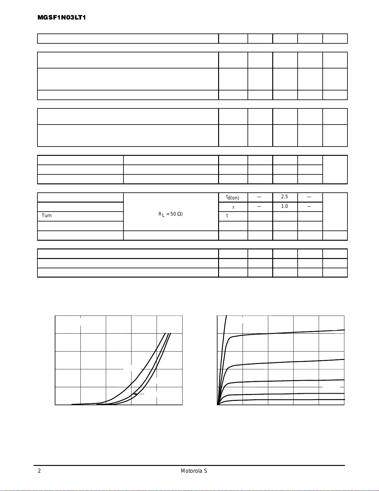
Figure 1. Transfer Characteristics Figure 2. On–Region Characteristics
0
1.5
2
0.5
1
1 1.5 2 2.5 3
I
D
, DRAIN CURRENT (AMPS)
VGS, GATE–TO–SOURCE VOLTAGE (VOLTS)
VDS = 10 V
TJ = 150°C
25°C
–55°C
3.5
2.5
0 2 4 10
0
1.5
2
VDS, DRAIN–TO–SOURCE VOLTAGE (VOLTS)
I
D
, DRAIN CURRENT (AMPS)
6
0.5
8
1
2.5
3.25 V
2.75 V
VGS = 3.75 V
2.5 V
3.0 V
3.5 V
(V
ns
 Loading...